


 |
市场调查报告书
商品编码
1699350
半导体计量及检测市场机会、成长动力、产业趋势分析及 2025-2034 年预测Semiconductor Metrology and Inspection Market Opportunity, Growth Drivers, Industry Trend Analysis, and Forecast 2025-2034 |
||||||
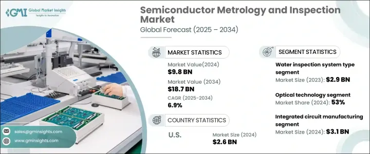
2024 年全球半导体计量和检测市场价值为 98 亿美元,预计 2025 年至 2034 年期间的复合年增长率为 6.9%。半导体製造流程的快速发展,加上对高性能晶片日益增长的需求,正在推动市场向前发展。随着晶片设计变得越来越复杂,晶体管尺寸越来越小,製造商在确保精度和可靠性方面面临越来越大的挑战。这导致对能够以奈米级精度检测缺陷的先进计量和检测系统的需求增加。汽车、消费性电子和电信等产业严重依赖这些解决方案来维持高生产良率并最大限度地减少製造过程中代价高昂的错误。
全球对半导体製造业的投资激增,特别是为应对供应链中断和地缘政治因素,正在推动市场成长。世界各国政府和私人企业正在扩大半导体製造设施,迫切需要精确的计量和检测系统。人工智慧、物联网和 5G 技术的兴起进一步扩大了对半导体元件的需求,因此需要采取严格的品质控制措施。此外,随着产业转向采用极紫外线 (EUV) 微影技术进行先进晶片生产,对能够在原子尺度上进行测量的计量工具的需求比以往任何时候都更加重要。
| 市场范围 | |
|---|---|
| 起始年份 | 2024 |
| 预测年份 | 2025-2034 |
| 起始值 | 98亿美元 |
| 预测值 | 187亿美元 |
| 复合年增长率 | 6.9% |
半导体计量和检测市场涵盖多个类别,包括晶圆检测系统、光罩检测系统、凸块检测、薄膜计量和引线框架检测。 2023年,晶圆检测系统占据了相当大的份额,价值达29亿美元。这些系统在识别半导体晶圆上的物理和图案缺陷方面发挥着至关重要的作用。透过捕捉精确的座标,製造商可以区分由污染物引起的随机缺陷和与曝光或掩模条件相关的系统缺陷。高精度检测缺陷的能力对于优化生产效率和提高半导体装置的品质至关重要。
市场也根据技术进行细分,其中光学、电子束和其他先进技术处于领先地位。预计光学技术将在 2024 年占据市场主导地位,占据 53% 的份额。光学计量解决方案因其能够以奈米精度测量和分析积体电路和半导体晶圆而被广泛采用,可确保光刻过程中的正确对准。它们能够捕捉微小缺陷,这使得它们在精度至关重要的现代半导体製造中不可或缺。
预计到 2034 年,德国半导体计量和检测市场规模将达到 11 亿美元。作为全球半导体供应链的关键参与者,德国继续大力投资先进製造解决方案。该国在汽车、工业和消费性电子产业的领导地位正在推动对高精度计量工具的需求。随着本地代工厂扩大业务,用于支援晶圆製造和先进封装的复杂计量和检测系统的需求预计将大幅增加。
目录
第一章:方法论与范围
- 市场范围和定义
- 基础估算与计算
- 预测计算
- 资料来源
- 基本的
- 次要
- 付费来源
- 公共资源
第二章:执行摘要
第三章:行业洞察
- 产业生态系统分析
- 影响价值链的因素
- 利润率分析
- 中断
- 未来展望
- 製造商
- 经销商
- 供应商格局
- 利润率分析
- 重要新闻和倡议
- 监管格局
- 衝击力
- 成长动力
- 半导体装置日益复杂
- 光刻技术的进步
- 消费性电子产品需求不断成长
- 对物联网和 5G 设备的需求不断增长
- 增加对半导体製造的投资
- 产业陷阱与挑战
- 先进设备成本高
- 与现有系统的整合问题
- 成长动力
- 成长潜力分析
- 波特的分析
- PESTEL分析
第四章:竞争格局
- 介绍
- 公司市占率分析
- 竞争定位矩阵
- 战略展望矩阵
第五章:市场估计与预测:依类型,2021-2034
- 主要趋势
- 晶圆检测系统
- 掩模检测系统
- 薄膜计量
- 碰撞检查
- 引线框架检查
第六章:市场估计与预测:依技术,2021-2034 年
- 主要趋势
- 光学的
- 电子束
- 其他的
第七章:市场估计与预测:按应用,2021-2034
- 主要趋势
- 积体电路製造
- 发光二极体 (LED) 製造
- 分立元件
- 包装和组装
- 其他的
第八章:市场估计与预测:依最终用途,2021-2034
- 主要趋势
- 半导体代工厂
- 整合设备製造商 (IDM)
- 第三方业务(OSAT)
- 研发机构
第九章:市场估计与预测:按地区,2021-2034
- 主要趋势
- 北美洲
- 我们
- 加拿大
- 欧洲
- 英国
- 德国
- 法国
- 义大利
- 西班牙
- 俄罗斯
- 亚太地区
- 中国
- 印度
- 日本
- 韩国
- 澳洲
- 拉丁美洲
- 巴西
- 墨西哥
- MEA
- 南非
- 沙乌地阿拉伯
- 阿联酋
第十章:公司简介
- Advantest Corporation
- Applied Materials, Inc.
- ASML Holding NV
- Bruker Corporation
- Camtek Ltd.
- Hitachi Ltd.
- JEOL Ltd.
- KLA Corporation
- Lasertec Corporation
- Nikon Corporation
- Nova Measuring Instruments Ltd.
- Olympus (EVIDENT)
- Onto Innovation, Inc
- Park Systems Corp.
- Thermo Fisher Scientific Inc.
- Toray Engineering Co., Ltd.
- Zygo Corporation
The Global Semiconductor Metrology And Inspection Market was valued at USD 9.8 billion in 2024 and is projected to expand at a CAGR of 6.9% from 2025 to 2034. The rapid evolution of semiconductor manufacturing processes, coupled with the growing demand for high-performance chips, is driving the market forward. As chip designs become more complex and transistor sizes shrink, manufacturers face increasing challenges in ensuring precision and reliability. This has led to a heightened demand for advanced metrology and inspection systems that can detect defects at nanometer-scale accuracy. Industries such as automotive, consumer electronics, and telecommunications rely heavily on these solutions to maintain high production yields and minimize costly errors in fabrication.
A surge in global investments in semiconductor manufacturing, particularly in response to supply chain disruptions and geopolitical factors, is fueling market growth. Governments and private enterprises worldwide are expanding semiconductor fabrication facilities, creating a pressing need for precise metrology and inspection systems. The rise of AI, IoT, and 5G technologies further amplifies the demand for semiconductor components, necessitating stringent quality control measures. Additionally, as the industry shifts toward extreme ultraviolet (EUV) lithography for advanced chip production, the need for metrology tools capable of measuring at the atomic scale is more critical than ever.
| Market Scope | |
|---|---|
| Start Year | 2024 |
| Forecast Year | 2025-2034 |
| Start Value | $9.8 Billion |
| Forecast Value | $18.7 Billion |
| CAGR | 6.9% |
The semiconductor metrology and inspection market encompasses various categories, including wafer inspection systems, mask inspection systems, bump inspection, thin film metrology, and lead frame inspection. In 2023, wafer inspection systems accounted for a substantial share, valued at USD 2.9 billion. These systems play a crucial role in identifying both physical and pattern defects on semiconductor wafers. By capturing precise coordinates, manufacturers can differentiate between random defects caused by contaminants and systematic defects related to exposure or mask conditions. The ability to detect defects with high precision is essential for optimizing production efficiency and enhancing the quality of semiconductor devices.
The market is also segmented based on technology, with optical, E-beam, and other advanced technologies leading the space. Optical technology is anticipated to dominate the market in 2024, securing a 53% share. Widely adopted due to its ability to measure and analyze integrated circuits and semiconductor wafers with nanometer accuracy, optical metrology solutions ensure proper alignment during the lithography process. Their capability to capture minute defects makes them indispensable in modern semiconductor manufacturing, where precision is paramount.
Germany semiconductor metrology and inspection market is projected to reach USD 1.1 billion by 2034. As a key player in the global semiconductor supply chain, Germany continues to invest heavily in advanced manufacturing solutions. The country's leadership in automotive, industrial, and consumer electronics industries is fueling the demand for high-precision metrology tools. With local foundries expanding operations, the need for sophisticated metrology and inspection systems to support wafer fabrication and advanced packaging is expected to rise significantly.
Table of Contents
Chapter 1 Methodology & Scope
- 1.1 Market scope & definitions
- 1.2 Base estimates & calculations
- 1.3 Forecast calculations
- 1.4 Data sources
- 1.4.1 Primary
- 1.4.2 Secondary
- 1.4.2.1 Paid sources
- 1.4.2.2 Public sources
Chapter 2 Executive Summary
- 2.1 Industry synopsis, 2021-2034
Chapter 3 Industry Insights
- 3.1 Industry ecosystem analysis
- 3.1.1 Factor affecting the value chain
- 3.1.2 Profit margin analysis
- 3.1.3 Disruptions
- 3.1.4 Future outlook
- 3.1.5 Manufacturers
- 3.1.6 Distributors
- 3.2 Supplier landscape
- 3.3 Profit margin analysis
- 3.4 Key news & initiatives
- 3.5 Regulatory landscape
- 3.6 Impact forces
- 3.6.1 Growth drivers
- 3.6.1.1 Increasing complexity of semiconductor devices
- 3.6.1.2 Advancements in lithography technologies
- 3.6.1.3 Rising consumer electronics demand
- 3.6.1.4 Rising demand for IoT and 5G-enabled devices
- 3.6.1.5 Increased investment in semiconductor manufacturing
- 3.6.2 Industry pitfalls & challenges
- 3.6.2.1 High cost of advanced equipment
- 3.6.2.2 Integration issues with existing systems
- 3.6.1 Growth drivers
- 3.7 Growth potential analysis
- 3.8 Porter's analysis
- 3.9 PESTEL analysis
Chapter 4 Competitive Landscape, 2024
- 4.1 Introduction
- 4.2 Company market share analysis
- 4.3 Competitive positioning matrix
- 4.4 Strategic outlook matrix
Chapter 5 Market Estimates & Forecast, By Type, 2021-2034 (USD Million)
- 5.1 Key trends
- 5.2 Wafer inspection system
- 5.3 Mask inspection system
- 5.4 Thin film metrology
- 5.5 Bump inspection
- 5.6 Lead frame inspection
Chapter 6 Market Estimates & Forecast, By Technology, 2021-2034 (USD Million)
- 6.1 Key trends
- 6.2 Optical
- 6.3 E-beam
- 6.4 Others
Chapter 7 Market Estimates & Forecast, By Application, 2021-2034 (USD Million)
- 7.1 Key trends
- 7.2 Integrated circuit manufacturing
- 7.3 Light Emitting Diode (LED) manufacturing
- 7.4 Discrete devices
- 7.5 Packaging and assembly
- 7.6 Others
Chapter 8 Market Estimates & Forecast, By End Use, 2021-2034 (USD Million)
- 8.1 Key trends
- 8.2 Semiconductor foundries
- 8.3 Integrated Device Manufacturers (IDMs)
- 8.4 Third-Party Business (OSAT)
- 8.5 Research & Development (R&D) institutions
Chapter 9 Market Estimates & Forecast, By Region, 2021-2034 (USD Million)
- 9.1 Key trends
- 9.2 North America
- 9.2.1 U.S.
- 9.2.2 Canada
- 9.3 Europe
- 9.3.1 UK
- 9.3.2 Germany
- 9.3.3 France
- 9.3.4 Italy
- 9.3.5 Spain
- 9.3.6 Russia
- 9.4 Asia Pacific
- 9.4.1 China
- 9.4.2 India
- 9.4.3 Japan
- 9.4.4 South Korea
- 9.4.5 Australia
- 9.5 Latin America
- 9.5.1 Brazil
- 9.5.2 Mexico
- 9.6 MEA
- 9.6.1 South Africa
- 9.6.2 Saudi Arabia
- 9.6.3 UAE
Chapter 10 Company Profiles
- 10.1 Advantest Corporation
- 10.2 Applied Materials, Inc.
- 10.3 ASML Holding N.V
- 10.4 Bruker Corporation
- 10.5 Camtek Ltd.
- 10.6 Hitachi Ltd.
- 10.7 JEOL Ltd.
- 10.8 KLA Corporation
- 10.9 Lasertec Corporation
- 10.10 Nikon Corporation
- 10.11 Nova Measuring Instruments Ltd.
- 10.12 Olympus (EVIDENT)
- 10.13 Onto Innovation, Inc
- 10.14 Park Systems Corp.
- 10.15 Thermo Fisher Scientific Inc.
- 10.16 Toray Engineering Co., Ltd.
- 10.17 Zygo Corporation
 半导体计量和检测设备市场-2025-2030年预测
 模具分类设备:全球市占率及排名、总收入及需求预测(2025-2031年)光罩检测和计量设备 - 全球市场份额和排名、总收入和需求预测(2025-2031 年)
 半导体计量和检测设备市场预测至2032年:按设备类型、技术、应用、最终用户和地区分類的全球分析
 2025年半导体计量和测试全球市场报告
 半导体计量和检测设备市场规模、份额和趋势分析报告:按技术、尺寸、製程节点、晶圆厂类型、地区和细分市场预测,2025 年至 2033 年
 全球半导体计量和测试市场
 半导体计量和测试设备:市场占有率分析、行业趋势、成长预测(2025-2030 年)
 曲线追踪器市场报告:趋势、预测和竞争分析(至 2031 年)
 半导体计量和测试市场按类型、技术类型、组件类型、最终用户、应用和行业细分 - 2025-2030 年全球预测