


 |
市场调查报告书
商品编码
1750314
硅外延晶圆市场机会、成长动力、产业趋势分析及2025-2034年预测Silicon EPI Wafer Market Opportunity, Growth Drivers, Industry Trend Analysis, and Forecast 2025 - 2034 |
||||||
2024年,全球硅外延晶圆市场规模达16亿美元,预计2034年将以13.2%的复合年增长率成长,达到55亿美元。这主要得益于汽车电子需求的不断增长、物联网和边缘运算设备的持续推广,以及全球半导体製造业的大规模投资。随着消费性电子、电动车和电信等领域晶片需求的激增,外延晶圆有助于提高设备效率并实现微型化。先进的逻辑积体电路、5G网路和基于人工智慧的技术正在加速普及,而国家政策支援和产业回流也在塑造未来成长方面发挥关键作用。
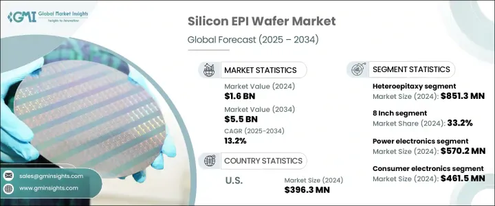
在美国,对来自关键地区的半导体进口产品征收关税扰乱了国内定价动态,并影响了全球竞争力。这些贸易行动增加了塑胶树脂和特殊金属等关键原料的成本,迫使企业重新评估全球供应链。儘管需要巨额资本投入,许多企业仍在迁移或考虑在地化生产。政府透过专门针对半导体的立法进行干预,透过提升国内晶圆製造能力并为新工厂提供财政激励,正在帮助缓解挑战。
| 市场范围 | |
|---|---|
| 起始年份 | 2024 |
| 预测年份 | 2025-2034 |
| 起始值 | 16亿美元 |
| 预测值 | 55亿美元 |
| 复合年增长率 | 13.2% |
2024年,异质外延领域市场规模达8.513亿美元,这得益于光电子元件、射频元件和先进CMOS技术领域对高效能半导体元件日益增长的需求。异质外延能够将不同晶格结构的材料(例如硅基硅锗)分层,为功率、速度和尺寸敏感型应用提供了更大的设计灵活性。随着3D整合和系统单晶片架构的日益普及,异质外延製程在实现能源效率和小型化目标方面的作用将变得更加重要。
2024年,8吋晶圆占据了33.2%的市场。此尺寸晶圆广泛应用于消费性电子和汽车半导体的生产,已成为主流。这些晶圆支持功率元件和感测器的经济高效的量产,尤其是在智慧型设备和电动车中。随着各行各业向数位化和智慧系统转型,对基于8吋晶圆的装置的需求持续成长。
2024年,美国硅外延晶圆市场规模达3.963亿美元,这得益于联邦政府对国内晶片製造的大力投资、电动汽车产量的不断增长以及人工智能和高性能计算(HPC)技术的日益融合。 5G、积体电路製造和汽车电子领域的先进应用刺激了本地需求,尤其是在企业寻求减少对海外供应商的依赖并建立具有韧性的区域生态系统的当下。
全球硅外延晶圆市场的主要参与者包括信越半导体(SEH)、世创电子(Siltronic)股份公司、胜高株式会社、SK Siltron 株式会社和环球晶圆株式会社。为了巩固市场地位,领导企业正在采取以产能扩张、技术创新和垂直整合为重点的策略。这些企业正在大力投资升级製造能力,并探索新的晶圆技术,以满足下一代设备不断变化的性能标准。与半导体製造商的策略合作确保了稳定的供应协议,而地理多元化则降低了与政治或贸易中断相关的风险。
目录
第一章:方法论与范围
第二章:执行摘要
第三章:行业洞察
- 产业生态系统分析
- 影响价值链的因素
- 利润率分析
- 中断
- 未来展望
- 製造商
- 经销商
- 川普政府关税
- 对贸易的影响
- 贸易量中断
- 报復措施
- 对产业的影响
- 供给侧影响(原料)
- 主要材料价格波动
- 供应链重组
- 生产成本影响
- 需求面影响(售价)
- 价格传导至终端市场
- 市占率动态
- 消费者反应模式
- 供给侧影响(原料)
- 受影响的主要公司
- 策略产业反应
- 供应链重组
- 定价和产品策略
- 政策参与
- 展望与未来考虑
- 对贸易的影响
- 供应商格局
- 利润率分析
- 重要新闻和倡议
- 监管格局
- 衝击力
- 成长动力
- 先进半导体装置需求激增
- 汽车电子的扩展
- 物联网和边缘设备的采用率不断提高
- 半导体製造投资不断成长
- 电力电子应用的成长
- 产业陷阱与挑战
- 外延生长的资本和营运成本高
- 严格的品质和缺陷控制要求
- 成长动力
- 成长潜力分析
- 波特的分析
- PESTEL分析
第四章:竞争格局
- 介绍
- 公司市占率分析
- 竞争定位矩阵
- 战略展望矩阵
第五章:市场估计与预测:依外延类型,2021-2034
- 主要趋势
- 异质外延
- 同质外延
第六章:市场预估与预测:依晶圆尺寸,2021-2034
- 主要趋势
- 6吋
- 8吋
- 12英吋
- 其他的
第七章:市场估计与预测:按应用,2021-2034
- 主要趋势
- 电力电子
- 微机电系统
- 射频电子元件
- 光子学
- 其他的
第八章:市场估计与预测:依最终用途,2021-2034
- 主要趋势
- 消费性电子产品
- 汽车
- 卫生保健
- 航太和国防
- 其他的
第九章:市场估计与预测:按地区,2021-2034
- 主要趋势
- 北美洲
- 我们
- 加拿大
- 欧洲
- 英国
- 德国
- 法国
- 义大利
- 西班牙
- 俄罗斯
- 亚太地区
- 中国
- 印度
- 日本
- 韩国
- 澳洲
- 拉丁美洲
- 巴西
- 墨西哥
- MEA
- 南非
- 沙乌地阿拉伯
- 阿联酋
第十章:公司简介
- Beijing Eswell Technology Group Co., Ltd.
- Coherent, Inc.
- Episil-Precision Inc.
- GlobalWafers Co., Ltd.
- IQE PLC
- Jenoptik AG
- MOSPEC Semiconductor Corporation
- NTT Advanced Technology Corporation
- Okmetic Oy
- Shanghai Simgui Technology Co., Ltd.
- Shin-Etsu Handotai
- Siltronic AG
- SK Siltron Co., Ltd.
- SOITEC SA
- SRI International
- SUMCO Corporation
- SweGaN AB
- Wafer Works Corporation
- Xiamen Powerway Advanced Material Co., Ltd
The Global Silicon EPI Wafer Market was valued at USD 1.6 billion in 2024 and is estimated to grow at a CAGR of 13.2% to reach USD 5.5 billion by 2034, driven by rising demand for automotive electronics, the continued rollout of IoT and edge computing devices, and massive investments in global semiconductor manufacturing. As chip demand surges across sectors like consumer electronics, electric vehicles, and telecommunications, epitaxial wafers help improve device efficiency and miniaturization. Advanced logic ICs, 5G networks, and AI-based technologies are accelerating adoption, while national policy support and industrial re-shoring efforts also play a crucial role in shaping future growth.
In the United States, the imposition of tariffs on semiconductor imports from key regions has disrupted domestic pricing dynamics and affected global competitiveness. These trade actions have increased costs for critical inputs like plastic resins and specialty metals, forcing companies to reassess global supply chains. Many firms are relocating or considering localizing production despite the heavy capital outlay required. Government intervention through semiconductor-specific legislation is helping mitigate challenges by boosting domestic wafer manufacturing capabilities and offering financial incentives for new plants.
| Market Scope | |
|---|---|
| Start Year | 2024 |
| Forecast Year | 2025-2034 |
| Start Value | $1.6 Billion |
| Forecast Value | $5.5 Billion |
| CAGR | 13.2% |
The heteroepitaxy segment generated USD 851.3 million in 2024, driven by the increasing need for high-performance semiconductor devices in optoelectronics, RF components, and advanced CMOS technology. The ability of heteroepitaxy to layer materials with differing lattice structures, such as silicon-germanium on silicon, offers greater design flexibility in power, speed, and size-sensitive applications. As 3D integration and system-on-chip architectures grow more prevalent, the role of heteroepitaxial processes will become even more essential to meet energy efficiency and miniaturization goals.
The 8-inch wafer category held a 33.2% market share in 2024. Its widespread use in the production of consumer electronics and automotive semiconductors has made this wafer size a mainstay. These wafers support cost-effective mass manufacturing of power devices and sensors, particularly those deployed in smart devices and electric vehicles. As industries shift toward digitalization and smarter systems, the demand for 8-inch wafer-based devices continues to rise.
U.S. Silicon EPI Wafer Market generated USD 396.3 million in 2024, bolstered by strong federal investment in domestic chip fabrication, rising EV production, and the growing integration of AI and HPC technologies. Advanced applications in 5G, IC manufacturing, and automotive electronics boost local demand, especially as companies seek to reduce reliance on overseas suppliers and build resilient regional ecosystems.
Key players in the Global Silicon EPI Wafer Market include Shin-Etsu Handotai (SEH), Siltronic AG, SUMCO Corporation, SK Siltron Co., Ltd., and GlobalWafers Co., Ltd. Strengthening their market presence, leading companies are adopting strategies that focus on capacity expansion, technological innovation, and vertical integration. Firms are heavily investing in upgrading manufacturing capabilities and exploring new wafer technologies that meet the evolving performance standards required for next-generation devices. Strategic collaborations with semiconductor manufacturers ensure steady supply agreements, while geographic diversification reduces risks related to political or trade disruptions.
Table of Contents
Chapter 1 Methodology & Scope
- 1.1 Market scope & definitions
- 1.2 Base estimates & calculations
- 1.3 Forecast calculations
- 1.4 Data sources
- 1.4.1 Primary
- 1.4.2 Secondary
- 1.4.2.1 Paid sources
- 1.4.2.2 Public sources
Chapter 2 Executive Summary
- 2.1 Industry synopsis, 2021-2034
Chapter 3 Industry Insights
- 3.1 Industry ecosystem analysis
- 3.1.1 Factor affecting the value chain
- 3.1.2 Profit margin analysis
- 3.1.3 Disruptions
- 3.1.4 Future outlook
- 3.1.5 Manufacturers
- 3.1.6 Distributors
- 3.2 Trump administration tariffs
- 3.2.1 Impact on trade
- 3.2.1.1 Trade volume disruptions
- 3.2.1.2 Retaliatory measures
- 3.2.1.3 Impact on the industry
- 3.2.1.3.1 Supply-side impact (raw materials)
- 3.2.1.3.1.1 Price volatility in key materials
- 3.2.1.3.1.2 Supply chain restructuring
- 3.2.1.3.1.3 Production cost implications
- 3.2.1.3.2 Demand-side impact (selling price)
- 3.2.1.3.2.1 Price transmission to end markets
- 3.2.1.3.2.2 Market share dynamics
- 3.2.1.3.2.3 Consumer response patterns
- 3.2.1.3.1 Supply-side impact (raw materials)
- 3.2.1.4 Key companies impacted
- 3.2.1.5 Strategic industry responses
- 3.2.1.5.1 Supply chain reconfiguration
- 3.2.1.5.2 Pricing and product strategies
- 3.2.1.5.3 Policy engagement
- 3.2.1.6 Outlook and future considerations
- 3.2.1 Impact on trade
- 3.3 Supplier landscape
- 3.4 Profit margin analysis
- 3.5 Key news & initiatives
- 3.6 Regulatory landscape
- 3.7 Impact forces
- 3.7.1 Growth drivers
- 3.7.1.1 Surge in demand for advanced semiconductor devices
- 3.7.1.2 Expansion of automotive electronics
- 3.7.1.3 Increasing adoption of IoT and edge devices
- 3.7.1.4 Growing investments in semiconductor manufacturing
- 3.7.1.5 Rising growth in power electronics applications
- 3.7.2 Industry pitfalls & challenges
- 3.7.2.1 High capital and operational costs of epitaxial growth
- 3.7.2.2 Stringent quality and defect control requirements
- 3.7.1 Growth drivers
- 3.8 Growth potential analysis
- 3.9 Porter's analysis
- 3.10 PESTEL analysis
Chapter 4 Competitive Landscape, 2024
- 4.1 Introduction
- 4.2 Company market share analysis
- 4.3 Competitive positioning matrix
- 4.4 Strategic outlook matrix
Chapter 5 Market Estimates & Forecast, By Epitaxy Type, 2021-2034 (USD Million & Units)
- 5.1 Key trends
- 5.2 Heteroepitaxy
- 5.3 Homoepitaxy
Chapter 6 Market Estimates & Forecast, By Wafer Size, 2021-2034 (USD Million & Units)
- 6.1 Key trends
- 6.2 6 inch
- 6.3 8 inch
- 6.4 12 inch
- 6.5 Others
Chapter 7 Market Estimates & Forecast, By Application, 2021-2034 (USD Million & Units)
- 7.1 Key trends
- 7.2 Power electronics
- 7.3 MEMS
- 7.4 RF electronics
- 7.5 Photonics
- 7.6 Others
Chapter 8 Market Estimates & Forecast, By End Use, 2021-2034 (USD Million & Units)
- 8.1 Key trends
- 8.2 Consumer electronics
- 8.3 Automotive
- 8.4 Healthcare
- 8.5 Aerospace and defense
- 8.6 Others
Chapter 9 Market Estimates & Forecast, By Region, 2021-2034 (USD Million & Units)
- 9.1 Key trends
- 9.2 North America
- 9.2.1 U.S.
- 9.2.2 Canada
- 9.3 Europe
- 9.3.1 UK
- 9.3.2 Germany
- 9.3.3 France
- 9.3.4 Italy
- 9.3.5 Spain
- 9.3.6 Russia
- 9.4 Asia Pacific
- 9.4.1 China
- 9.4.2 India
- 9.4.3 Japan
- 9.4.4 South Korea
- 9.4.5 Australia
- 9.5 Latin America
- 9.5.1 Brazil
- 9.5.2 Mexico
- 9.6 MEA
- 9.6.1 South Africa
- 9.6.2 Saudi Arabia
- 9.6.3 UAE
Chapter 10 Company Profiles
- 10.1 Beijing Eswell Technology Group Co., Ltd.
- 10.2 Coherent, Inc.
- 10.3 Episil-Precision Inc.
- 10.4 GlobalWafers Co., Ltd.
- 10.5 IQE PLC
- 10.6 Jenoptik AG
- 10.7 MOSPEC Semiconductor Corporation
- 10.8 NTT Advanced Technology Corporation
- 10.9 Okmetic Oy
- 10.10 Shanghai Simgui Technology Co., Ltd.
- 10.11 Shin-Etsu Handotai
- 10.12 Siltronic AG
- 10.13 SK Siltron Co., Ltd.
- 10.14 SOITEC SA
- 10.15 SRI International
- 10.16 SUMCO Corporation
- 10.17 SweGaN AB
- 10.18 Wafer Works Corporation
- 10.19 Xiamen Powerway Advanced Material Co., Ltd
 外延晶片市场规模、份额、趋势及预测(按类型、晶片尺寸、应用、产业及地区划分),2026-2034年
 2026年全球硅外延晶片市场报告
 外延晶片市场-2026-2031年预测
 外延晶片市场:按类型、应用、终端用户产业、国家及地区划分 - 全球产业分析、市场规模、市场占有率及2025-2032年预测
 外延晶片市场规模、份额和成长分析(按类型、晶片尺寸、沉积方法、应用、最终用途产业和地区划分)-2026-2033年产业预测
 氮化镓外延:全球市场份额和排名、总收入和需求预测(2025-2031 年)
 全球外延片市场全球化合物半导体外延片市场全球硅外延晶圆市场全球外延晶圆和晶片技术市场