


 |
市场调查报告书
商品编码
1750500
砷化硼(BAs)市场机会、成长动力、产业趋势分析及2025-2034年预测Boron Arsenide (BAs) Market Opportunity, Growth Drivers, Industry Trend Analysis, and Forecast 2025 - 2034 |
||||||
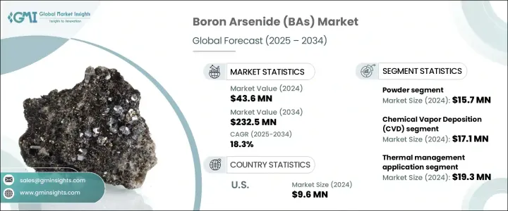
2024 年全球砷化硼 (BA) 市值为 4,360 万美元,预计到 2034 年将以 18.3% 的复合年增长率成长,达到 2.325 亿美元。这一令人印象深刻的成长是由各种高性能应用对先进半导体材料不断增长的需求所推动的。随着工业界越来越重视小型化、高频操作和热效率,砷化硼因其优异的导热性和优越的载子迁移率而成为首选材料。从电信和消费性电子产品到能源系统和国防技术,高性能半导体的整合已成为产品创新和能源优化的核心。随着硅等传统材料接近其性能极限,工业界逐渐转向具有更好耐用性和运作效率的替代品。砷化硼凭藉其独特的物理特性,作为推动向下一代电子产品过渡的关键材料之一,正日益受到关注。
从历史上看,向化合物半导体的转变源于人们对在高应力工作条件下性能优于硅的材料的需求。砷化硼以及其他替代材料正被研究作为这项转变的可靠解决方案。随着人们不断探索能够在严苛环境下高效运作的材料,砷化硼在多个应用领域不断证明其实用性。
| 市场范围 | |
|---|---|
| 起始年份 | 2024 |
| 预测年份 | 2025-2034 |
| 起始值 | 4360万美元 |
| 预测值 | 2.325亿美元 |
| 复合年增长率 | 18.3% |
在各产品领域中,砷化硼粉末占据最大份额,2024年的估值为1570万美元。预计该领域在2025年至2034年期间的复合年增长率将达到17.7%。此类别的稳定成长主要归功于其在积层製造和粉末冶金领域的不断扩展。复合材料的发展也对粉末领域的成长起到了推动作用,因为製造商正在寻求稳定且导热的物质,以将其整合到现代能源系统和电子产品中。
晶体砷化硼因其卓越的结构完整性和在高频工作条件下的性能而日益受到欢迎。随着电子设备变得越来越紧凑和强大,对晶体形式的需求也在不断增长,这反映了向微型化和高效系统的转变。这一趋势是由对能够支援高级功能且不牺牲热管理或性能稳定性的半导体日益增长的需求所驱动。
砷化硼薄膜在柔性电子和光子学领域正变得至关重要。其在高温下的适应性和可靠性使其非常适合应用于不断发展的电子设备。随着各行各业逐渐转向轻量化、高效的技术,例如穿戴式装置和柔性显示器,薄膜市场正在迅速扩张。薄膜凭藉其高效率和最小能量损耗,促进了紧凑型电子产品的进步,进一步将砷化硼定位为面向未来的材料。
化学气相沉积 (CVD) 是 2024 年最大的技术领域,价值 1,710 万美元,预计在预测期内将以 17.3% 的复合年增长率增长。对精密工程材料日益增长的需求提升了 CVD 在高性能半导体生产中的作用。这种方法因其生产效率更高、均匀性和结构稳定性更高而越来越受到青睐,以满足尖端半导体应用的需求。
高压高温 (HPHT) 合成对于生产用于航太和国防系统的高纯度砷化硼晶体至关重要。该製程能够形成能够承受极端环境条件的大型无缺陷晶体。随着这些产业追求先进的热处理和结构解决方案,HPHT 合成材料的相关性不断提升,从而支持市场进一步扩张。
在应用方面,热管理在2024年达到1,930万美元,预计2025年至2034年的复合年增长率为18%。该领域占据了44.1%的主导市场。砷化硼卓越的导热性使其成为高性能电子设备中热量管理的宝贵资产,并有望显着提高系统的能源效率。随着现代电子元件日益复杂,有效散热已成为当务之急,而砷化硼为紧凑型高输出设备中的冷却机制提供了极具吸引力的解决方案。
随着高效热控制需求的持续成长,砷化硼在运算环境中(包括资料中心和下一代电子设备)的使用预计将大幅成长。随着全球数位基础设施的扩张和运算需求的不断增长,砷化硼在改善冷却系统中的作用日益重要。
在美国,砷化硼的国内产量仍然有限,导致依赖进口材料来满足日益增长的需求。这种供应动态凸显了确保高纯度半导体材料对支援多个产业技术进步的策略重要性。虽然历史上进口可以满足消费需求,但不断增长的国内应用正促使美国探索内部製造和采购策略。
在全球范围内,砷化硼市场正在快速成长,尤其是在亚太地区,该地区目前占据最大份额。主要参与者正在加强投资力度,以增强砷化硼材料的供应链和生产能力,以满足电子、能源、航太和电信业日益增长的需求。随着半导体和再生能源领域的持续创新和资本流入,砷化硼市场预计将在未来十年保持强劲成长动能。
目录
第一章:方法论与范围
第二章:执行摘要
第三章:行业洞察
- 产业生态系统分析
- 影响价值链的因素
- 利润率分析
- 中断
- 前景
- 製造商
- 经销商
- 川普政府关税
- 对贸易的影响
- 贸易量中断
- 报復措施
- 对产业的影响
- 供应方影响(原料)
- 主要材料价格波动
- 供应链重组
- 生产成本影响
- 需求面影响(售价)
- 价格传导至终端市场
- 市占率动态
- 消费者反应模式
- 供应方影响(原料)
- 受影响的主要公司
- 策略产业反应
- 供应链重组
- 定价和产品策略
- 政策参与
- 展望与未来考虑
- 对贸易的影响
- 贸易统计(HS编码)
- 主要出口国
- 主要进口国
- 利润率分析
- 重要新闻和倡议
- 监管格局
- 衝击力
- 成长动力
- 电子业对高导热材料的需求不断增加
- 半导体和光电子元件製造技术的快速进步
- 紧凑型电子产品对高效热管理解决方案的需求日益增长
- 砷化硼在下一代电晶体和晶片冷却的应用日益增多
- 产业陷阱与挑战
- 砷化硼合成和纯化的生产成本高
- 大规模商业可用性有限和供应链限制
- 成长动力
- 成长潜力分析
- 波特的分析
- PESTEL分析
第四章:竞争格局
- 竞争格局
- 公司概况
- 产品组合和规格
- SWOT分析
- 公司市占率分析
- 全球市场占有率(按公司划分)
- 区域市占率分析
- 产品组合份额分析
- 策略倡议
- 併购
- 伙伴关係和合作
- 产品发布和创新
- 扩张计划和投资
- 公司标竿分析
- 产品创新标桿
- 定价策略比较
- 配电网路比较
- 客户服务和支援比较
第五章:市场估计与预测:依形式,2021-2034
- 主要趋势
- 粉末
- 奈米粉末
- 微粉
- 其他粉末形式
- 水晶
- 单晶
- 多晶硅
- 薄膜
- 散装材料
- 其他形式
第六章:市场估计与预测:依纯度等级,2021-2034
- 主要趋势
- <99%
- 99% - 99.9%
- 99.9% - 99.99%
- > 99.99%
第七章:市场估计与预测:依生产方式,2021-2034 年
- 主要趋势
- 化学气相沉积(CVD)
- 常压化学气相沉积
- 低压化学气相沉积
- 等离子增强化学气相沉积
- 高压高温(HPHT)合成
- 分子束外延(MBE)
- 助熔剂生长法
- 其他生产方法
第 8 章:市场估计与预测:按应用,2021 年至 2034 年
- 主要趋势
- 热管理
- 散热器
- 热界面材料
- 散热器
- 其他热管理应用
- 电子冷却
- 高功率电子设备
- 资料中心
- 消费性电子产品
- 其他电子冷却应用
- 半导体装置
- 电力电子
- 光电子
- 高频设备
- 其他半导体应用
- 研究与开发
- 其他应用
第九章:市场估计与预测:依最终用途产业,2021-2034 年
- 主要趋势
- 电子和半导体
- 积体电路製造商
- 电子元件製造商
- 半导体设备製造商
- 电信
- 汽车与运输
- 电动车
- 传统车辆
- 航太与国防
- 能源与电力
- 工业设备
- 研究机构和学术界
- 其他最终用途产业
第十章:市场估计与预测:按地区,2021-2034
- 主要趋势
- 北美洲
- 我们
- 加拿大
- 欧洲
- 德国
- 英国
- 法国
- 西班牙
- 义大利
- 欧洲其他地区
- 亚太地区
- 中国
- 印度
- 日本
- 澳洲
- 韩国
- 亚太其他地区
- 拉丁美洲
- 巴西
- 墨西哥
- 阿根廷
- 拉丁美洲其他地区
- 中东和非洲
- 沙乌地阿拉伯
- 南非
- 阿联酋
- 中东和非洲其他地区
第 11 章:公司简介
- II-VI Incorporated
- Momentive Performance Materials Inc.
- KYMA Technologies, Inc.
- American Elements
- Nanoshel LLC
- Stanford Advanced Materials
- SkySpring Nanomaterials, Inc.
- Alfa Aesar (Thermo Fisher Scientific)
- Materion Corporation
- DOWA Electronics Materials Co., Ltd.
- Shin-Etsu Chemical Co., Ltd.
- Sumitomo Electric Industries, Ltd.
- Heraeus Holding GmbH
- Indium Corporation
- Others
The Global Boron Arsenide (BAs) Market was valued at USD 43.6 million in 2024 and is estimated to grow at a CAGR of 18.3% to reach USD 232.5 million by 2034. This impressive expansion is fueled by the rising demand for advanced semiconductor materials across various high-performance applications. As industries increasingly prioritize miniaturization, high-frequency operations, and thermal efficiency, boron arsenide has emerged as a material of choice due to its outstanding thermal conductivity and superior carrier mobility. From telecommunications and consumer electronics to energy systems and defense technologies, the integration of high-performance semiconductors has become central to product innovation and energy optimization. As traditional materials such as silicon near their performance limits, industries are gradually turning to alternatives that offer better durability and operational efficiency. Boron arsenide, with its unique physical properties, is gaining traction as one of the key materials driving the transition toward next-generation electronics.
Historically, the switch to compound semiconductors was motivated by the need for materials that outperform silicon under high-stress operational conditions. Boron arsenide, along with other alternatives, is being investigated as a reliable solution in this shift. With the ongoing exploration of materials that can function efficiently in demanding environments, boron arsenide continues to prove its utility in multiple application areas.
| Market Scope | |
|---|---|
| Start Year | 2024 |
| Forecast Year | 2025-2034 |
| Start Value | $43.6 Million |
| Forecast Value | $232.5 Million |
| CAGR | 18.3% |
Among product segments, boron arsenide powder represented the largest share, with a valuation of USD 15.7 million in 2024. This segment is expected to witness a CAGR of 17.7% from 2025 to 2034. The steady growth of this category is primarily attributed to its expanding use in additive manufacturing and powder metallurgy. The development of composite materials also plays a role in supporting the powder segment's rise, as manufacturers seek stable and thermally conductive substances for integration into modern energy systems and electronics.
Crystalline boron arsenide is also gaining popularity due to its exceptional structural integrity and ability to perform under high-frequency operating conditions. The demand for crystal forms is rising as electronic devices become more compact and powerful, reflecting the shift toward miniaturized yet high-efficiency systems. This trend is driven by the growing need for semiconductors that can support advanced functionality without sacrificing thermal management or performance stability.
Thin films of boron arsenide are becoming essential in flexible electronics and photonics. Their adaptability and reliability at elevated temperatures make them suitable for incorporation into evolving electronic devices. With industries leaning toward lightweight, efficient technologies such as wearable devices and flexible displays, the thin film segment is expanding rapidly. Thin films are contributing to the advancement of compact electronics by offering high efficiency with minimal energy loss, further positioning boron arsenide as a future-forward material.
Chemical vapor deposition (CVD) was the largest technology segment in 2024, valued at USD 17.1 million, and is forecasted to expand at a CAGR of 17.3% during the forecast period. The growing need for precision-engineered materials has elevated the role of CVD in the production of high-performance semiconductors. This method is increasingly favored for producing materials with enhanced efficiency, uniformity, and structural stability, aligning with the demands of cutting-edge semiconductor applications.
High-pressure high-temperature (HPHT) synthesis is crucial for producing high-purity boron arsenide crystals used in aerospace and defense systems. This process allows for the formation of large, defect-free crystals capable of withstanding extreme environmental conditions. As these industries pursue advanced thermal and structural solutions, the relevance of HPHT-produced materials continues to rise, supporting further market expansion.
In terms of application, thermal management accounted for USD 19.3 million in 2024, with a projected CAGR of 18% between 2025 and 2034. This segment held a dominant market share of 44.1%. The exceptional thermal conductivity of boron arsenide makes it a valuable asset in managing heat in high-performance electronics, offering the potential to significantly improve the energy efficiency of systems. With the rising complexity of modern electronic components, effective heat dissipation has become a priority, and boron arsenide offers a compelling solution for cooling mechanisms in compact, high-output devices.
The use of boron arsenide is also expected to grow significantly in computing environments, including data centers and next-gen electronics, as the demand for efficient thermal control continues to accelerate. As global digital infrastructure expands and computing demands intensify, the role of boron arsenide in improving cooling systems becomes increasingly important.
In the United States, domestic production of boron arsenide remains limited, resulting in a reliance on imported materials to meet growing demand. This supply dynamic underlines the strategic importance of securing high-purity semiconductor materials to support technological advancements across multiple sectors. While imports have historically met consumption needs, rising domestic applications are pushing the U.S. to explore internal manufacturing and sourcing strategies.
Globally, the boron arsenide market is witnessing rapid growth, particularly in the Asia Pacific region, which currently holds the largest share. Key players are channeling investments into enhancing the supply chain and production capabilities for boron arsenide materials to meet the increasing demands across electronics, energy, aerospace, and telecommunication industries. With continued innovations and capital inflows into semiconductor and renewable energy sectors, the momentum behind boron arsenide is expected to remain strong throughout the next decade.
Table of Contents
Chapter 1 Methodology & Scope
- 1.1 Market scope & definitions
- 1.2 Base estimates & calculations
- 1.3 Forecast calculations
- 1.4 Data sources
- 1.4.1 Primary
- 1.4.2 Secondary
- 1.4.2.1 Paid sources
- 1.4.2.2 Public sources
Chapter 2 Executive Summary
- 2.1 Industry synopsis, 2021-2034
Chapter 3 Industry Insights
- 3.1 Industry ecosystem analysis
- 3.1.1 Factor affecting the value chain
- 3.1.2 Profit margin analysis
- 3.1.3 Disruptions
- 3.1.4 Outlook
- 3.1.5 Manufacturers
- 3.1.6 Distributors
- 3.2 Trump administration tariffs
- 3.2.1 Impact on trade
- 3.2.1.1 Trade volume disruptions
- 3.2.1.2 Retaliatory measures
- 3.2.2 Impact on the industry
- 3.2.2.1 Supply-side impact (raw materials)
- 3.2.2.1.1 Price volatility in key materials
- 3.2.2.1.2 Supply chain restructuring
- 3.2.2.1.3 Production cost implications
- 3.2.2.2 Demand-side impact (selling price)
- 3.2.2.2.1 Price transmission to end markets
- 3.2.2.2.2 Market share dynamics
- 3.2.2.2.3 Consumer response patterns
- 3.2.2.1 Supply-side impact (raw materials)
- 3.2.3 Key companies impacted
- 3.2.4 Strategic industry responses
- 3.2.4.1 Supply chain reconfiguration
- 3.2.4.2 Pricing and product strategies
- 3.2.4.3 Policy engagement
- 3.2.5 Outlook and Future Considerations
- 3.2.1 Impact on trade
- 3.3 Trade statistics (HS Code)
- 3.3.1 Major exporting countries
- 3.3.2 Major importing countries
- 3.4 Profit margin analysis
- 3.5 Key news & initiatives
- 3.6 Regulatory landscape
- 3.7 Impact forces
- 3.7.1 Growth drivers
- 3.7.1.1 Increasing demand for high thermal conductivity materials in electronics industry
- 3.7.1.2 Rapid advancements in semiconductor and optoelectronic device manufacturing technologies
- 3.7.1.3 Growing need for efficient thermal management solutions in compact electronics
- 3.7.1.4 Rising adoption of boron arsenide in next-gen transistors and chip cooling
- 3.7.2 Industry pitfalls & challenges
- 3.7.2.1 High production costs associated with boron arsenide synthesis and purification
- 3.7.2.2 Limited large-scale commercial availability and supply chain constraints
- 3.7.1 Growth drivers
- 3.8 Growth potential analysis
- 3.9 Porter's analysis
- 3.10 PESTEL analysis
Chapter 4 Competitive Landscape, 2024
- 4.1 Competitive landscape
- 4.1.1 Company overview
- 4.1.2 Product portfolio and specifications
- 4.1.3 Swot analysis
- 4.2 Company market share analysis, 2024
- 4.2.1 Global market share by company
- 4.2.2 Regional market share analysis
- 4.2.3 Product portfolio share analysis
- 4.3 Strategic initiative
- 4.3.1 Mergers and acquisitions
- 4.3.2 Partnerships and collaborations
- 4.3.3 Product launches and innovations
- 4.3.4 Expansion plans and investments
- 4.4 Company benchmarking
- 4.4.1 Product innovation benchmarking
- 4.4.2 Pricing strategy comparison
- 4.4.3 Distribution network comparison
- 4.4.4 Customer service and support comparison
Chapter 5 Market Estimates & Forecast, By Form, 2021-2034 (USD Million) (Kilo Tons)
- 5.1 Key trends
- 5.2 Powder
- 5.2.1 Nano powder
- 5.2.2 Micro powder
- 5.2.3 Other powder forms
- 5.3 Crystal
- 5.3.1 Single crystal
- 5.3.2 Polycrystalline
- 5.3.3 Thin film
- 5.4 Bulk material
- 5.5 Other forms
Chapter 6 Market Estimates & Forecast, By Purity Level, 2021-2034 (USD Million) (Kilo Tons)
- 6.1 Key trends
- 6.2 <99%
- 6.3 99% - 99.9%
- 6.4 99.9% - 99.99%
- 6.5 > 99.99%
Chapter 7 Market Estimates & Forecast, By Production Method, 2021-2034 (USD Million) (Kilo Tons)
- 7.1 Key trends
- 7.2 Chemical vapor deposition (CVD)
- 7.2.1 Atmospheric pressure CVD
- 7.2.2 Low pressure CVD
- 7.2.3 Plasma-enhanced CVD
- 7.3 High-pressure high-temperature (HPHT) synthesis
- 7.4 Molecular beam epitaxy (MBE)
- 7.5 Flux growth method
- 7.6 Other production methods
Chapter 8 Market Estimates & Forecast, By Application, 2021-2034 (USD Million) (Kilo Tons)
- 8.1 Key trends
- 8.2 Thermal management
- 8.2.1 Heat sinks
- 8.2.2 Thermal interface materials
- 8.2.3 Heat spreaders
- 8.2.4 Other thermal management applications
- 8.3 Electronics cooling
- 8.3.1 High-power electronics
- 8.3.2 Data centers
- 8.3.3 Consumer electronics
- 8.3.4 Other electronics cooling applications
- 8.4 Semiconductor devices
- 8.4.1 Power electronics
- 8.4.2 Optoelectronics
- 8.4.3 High-frequency devices
- 8.4.4 Other semiconductor applications
- 8.5 Research & development
- 8.6 Other applications
Chapter 9 Market Estimates & Forecast, By End Use Industry, 2021-2034 (USD Million) (Kilo Tons)
- 9.1 Key trends
- 9.2 Electronics & semiconductor
- 9.2.1 Integrated circuit manufacturers
- 9.2.2 Electronic component manufacturers
- 9.2.3 Semiconductor equipment manufacturers
- 9.3 Telecommunications
- 9.4 Automotive & transportation
- 9.4.1 Electric vehicles
- 9.4.2 Conventional vehicles
- 9.4.3 Aerospace & defense
- 9.5 Energy & power
- 9.6 Industrial equipment
- 9.7 Research institutions & academia
- 9.8 Other end use industries
Chapter 10 Market Estimates & Forecast, By Region, 2021-2034 (USD Million) (Kilo Tons)
- 10.1 Key trends
- 10.2 North America
- 10.2.1 U.S.
- 10.2.2 Canada
- 10.3 Europe
- 10.3.1 Germany
- 10.3.2 UK
- 10.3.3 France
- 10.3.4 Spain
- 10.3.5 Italy
- 10.3.6 Rest of Europe
- 10.4 Asia Pacific
- 10.4.1 China
- 10.4.2 India
- 10.4.3 Japan
- 10.4.4 Australia
- 10.4.5 South Korea
- 10.4.6 Rest of Asia Pacific
- 10.5 Latin America
- 10.5.1 Brazil
- 10.5.2 Mexico
- 10.5.3 Argentina
- 10.5.4 Rest of Latin America
- 10.6 Middle East and Africa
- 10.6.1 Saudi Arabia
- 10.6.2 South Africa
- 10.6.3 UAE
- 10.6.4 Rest of Middle East and Africa
Chapter 11 Company Profiles
- 11.1 II-VI Incorporated
- 11.2 Momentive Performance Materials Inc.
- 11.3 KYMA Technologies, Inc.
- 11.4 American Elements
- 11.5 Nanoshel LLC
- 11.6 Stanford Advanced Materials
- 11.7 SkySpring Nanomaterials, Inc.
- 11.8 Alfa Aesar (Thermo Fisher Scientific)
- 11.9 Materion Corporation
- 11.10 DOWA Electronics Materials Co., Ltd.
- 11.11 Shin-Etsu Chemical Co., Ltd.
- 11.12 Sumitomo Electric Industries, Ltd.
- 11.13 Heraeus Holding GmbH
- 11.14 Indium Corporation
- 11.15 Others
