


 |
市场调查报告书
商品编码
1773475
硫族化物(MoS2、WS2、WSe2)市场机会、成长动力、产业趋势分析及 2025 - 2034 年预测Chalcogenides (MoS2, WS2, WSe2) Market Opportunity, Growth Drivers, Industry Trend Analysis, and Forecast 2025 - 2034 |
||||||
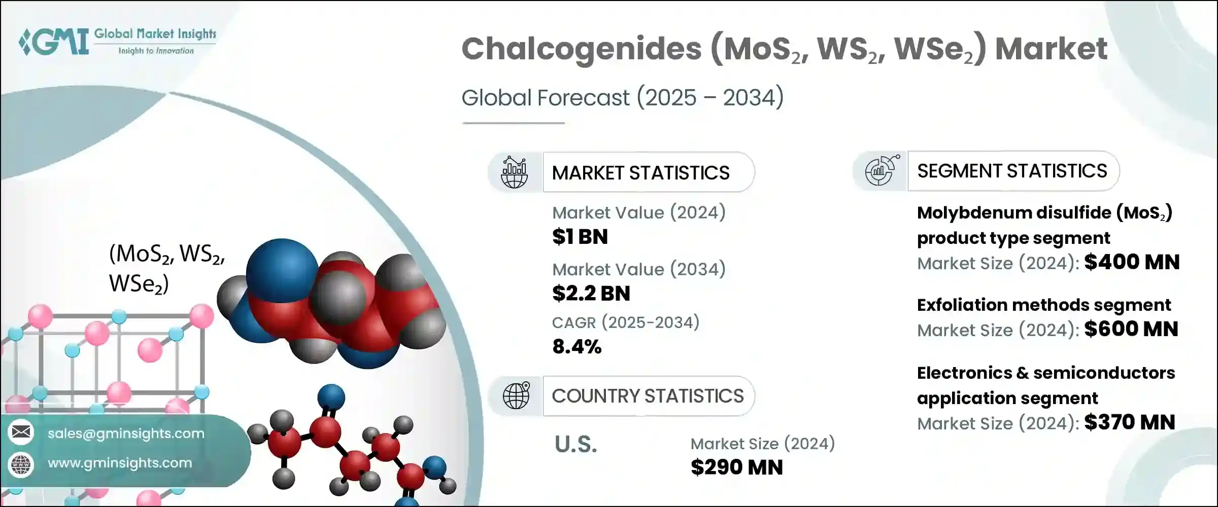
2024 年全球硫族化物(MoS2、WS2、WSe2)市场价值为 10 亿美元,预计到 2034 年将以 8.4% 的复合年增长率增长至 22 亿美元。这种稳定成长反映了先进材料领域的广泛发展势头,这一领域受到奈米技术的发展以及多个垂直领域对高性能、节能解决方案日益增长的需求的推动。这些层状过渡金属二硫族化物由于其卓越的电气、机械和光学性能,已成为未来电子产品的关键推动因素。由于传统的硅基技术遇到物理和缩放限制,这些二维材料正成为微型电子产品、柔性设备和高速电晶体等应用领域的有希望的替代品。人们对紧凑且节能的硬体日益增长的兴趣在航太、国防、电信和医疗设备等领域尤为重要。
包括美国、亚太地区和欧盟在内的各地区政府支持的研发计画正在提供关键的资金和机构支持,以推动下一代材料创新。这些计划包括建立国家创新中心、资助试点製造中心以及支持实验室规模研究的商业化。公私合作伙伴关係正在加强,尤其是在半导体和再生能源领域,将二维半导体整合到柔性基板中正变得越来越可行。该行业正在响应对更快、更小、更节能的晶片日益增长的需求,而二硫化钼和二氧化钨等材料由于其可调带隙和卓越的载流子迁移率,相比传统材料具有显着的性能优势。
| 市场范围 | |
|---|---|
| 起始年份 | 2024 |
| 预测年份 | 2025-2034 |
| 起始值 | 10亿美元 |
| 预测值 | 22亿美元 |
| 复合年增长率 | 8.4% |
在製造技术中,剥离法细分市场在2024年创造了6亿美元的市场规模,预计到2034年将以7.9%的复合年增长率成长。虽然剥离法对于研究级材料和原型仍然至关重要,但化学气相沉积 (CVD) 技术因其能够产生与商用级半导体製程相容的均匀高品质薄膜,正日益成为可扩展生产领域的主导。 CVD 技术能够实现精确的层控制、广泛的基材相容性以及工业规模的可重复性,使其成为从研发过渡到高通量电子製造的首选技术。许多製造实验室和中试设施已采用 CVD 技术,凸显了其在连接实验室创新与奈米材料商业规模应用方面的关键作用。
电子和半导体领域在2024年创造了可观的收入。其独特的能带结构和半导体特性使其成为先进场效电晶体、储存元件和薄膜逻辑电路的理想候选材料。这些材料具有前所未有的灵活性和超薄架构,使其成为下一代穿戴式技术、整合光子学和软体机器人的理想选择。研究人员已经报告了其开关行为和阈值性能,其性能堪比甚至超越了规模化硅基器件,这促使各大半导体製造商在迈向后摩尔定律设计时代之际,纷纷探索这些二维替代方案。
预计在2025年至2034年期间,美国硫族化合物(二硫化钼、二硫化钨和二硒化钨)市场将以显着的复合年增长率成长,这主要得益于研发投入,尤其是在量子技术和国防级半导体领域的应用。儘管二硫化钼和二硒化钨等块状材料主要从亚洲进口,但美国在下游开发和整合方面处于领先地位,并向国际市场出口增值衍生物。美国的高科技产业将这些材料应用于尖端原型设计,不断突破光电子学、光子学和下一代电晶体架构的界限。 ACS Material和2D Tech等公司在推动国内研究工作方面发挥关键作用,而大型国防承包商和电子产品製造商则推动对这些高性能奈米材料的需求。
全球硫族化物(MoS2、WS2、WSe2)市场知名的企业包括SixCarbon Technology、Graphene Laboratories Inc.、American Elements、ACS Material LLC和XFNANO Materials Tech Co., Ltd.。这些公司对于材料合成和供应链开发都至关重要。为了提升市场地位并扩大全球影响力,硫族化物产业的领导企业正在采取多种策略。他们正在扩大生产能力以满足日益增长的工业和商业需求,同时继续投资于高精度材料表征和客製化。与学术机构和国家实验室的合作有助于促进尖端创新,尤其是在量子应用和柔性电子领域。主要企业也正在与设备製造商建立策略合作伙伴关係,共同开发使用二维材料的特定应用解决方案。
目录
第一章:方法论
- 市场范围和定义
- 研究设计
- 研究方法
- 资料收集方法
- 资料探勘来源
- 全球的
- 地区/国家
- 基础估算与计算
- 基准年计算
- 市场评估的主要趋势
- 初步研究和验证
- 主要来源
- 预测模型
- 研究假设和局限性
第二章:执行摘要
第三章:行业洞察
- 产业生态系统分析
- 供应商概况
- 利润率
- 每个阶段的增值
- 影响价值链的因素
- 中断
- 产业衝击力
- 成长动力
- 产业陷阱与挑战
- 市场机会
- 成长潜力分析
- 监管格局
- 北美洲
- 欧洲
- 亚太地区
- 拉丁美洲
- 中东和非洲
- 波特的分析
- PESTEL分析
- 价格趋势
- 按地区
- 按产品
- 未来市场趋势
- 技术和创新格局
- 当前的技术趋势
- 新兴技术
- 专利态势
- 贸易统计资料(HS 编码)(註:仅提供主要国家的贸易统计数据
- 主要进口国
- 主要出口国
- 永续性和环境方面
- 永续实践
- 减少废弃物的策略
- 生产中的能源效率
- 环保倡议
- 碳足迹考量
第四章:竞争格局
- 介绍
- 公司市占率分析
- 按地区
- 北美洲
- 欧洲
- 亚太地区
- 拉丁美洲
- MEA
- 按地区
- 公司矩阵分析
- 主要市场参与者的竞争分析
- 竞争定位矩阵
- 关键进展
- 併购
- 伙伴关係与合作
- 新产品发布
- 扩张计划
第五章:市场估计与预测:依材料类型,2021-2034
- 主要趋势
- 二硫化钼(MoS2)
- 二硫化钨(WS2)
- 二硒化钨(WSe2)
- 异质结构和混合结构
- 其他的
第六章:市场估计与预测:依合成与製造技术,2021-2034 年
- 主要趋势
- 去角质方法
- 机械剥落
- 液相剥离
- 电化学剥离
- 插层辅助剥离
- 其他的
- 化学气相沉积(CVD)
- 传统 CVD 工艺
- 金属有机化学气相沉积 (MOCVD)
- 物理气相沉积(PVD)
- 溅镀技术
- 脉衝雷射沉积
- 可扩展的生产方法
- 化学合成路线
- 其他的
第七章:市场估计与预测:按应用,2021-2034
- 主要趋势
- 电子和半导体
- 场效电晶体(FET)
- 逻辑闸和电路
- 储存装置
- 柔性电子产品
- 其他的
- 光电子学与光子学
- 光电探测器
- 发光二极体 (LED)
- 电致发光装置
- 太阳能电池/光伏
- 其他的
- 能量储存与转换
- 可充电电池
- 超级电容器
- 析氢反应(HER)催化剂
- 二氧化碳还原催化剂
- 热电器件
- 燃料电池
- 其他的
- 感测器和探测器
- 气体感测器
- 生物感测器
- 压力和应变感测器
- 其他的
- 量子技术
- 摩擦学和润滑剂
- 生物医学应用
- 其他的
第八章:市场估计与预测:按地区,2021-2034
- 主要趋势
- 北美洲
- 我们
- 加拿大
- 欧洲
- 德国
- 英国
- 法国
- 义大利
- 西班牙
- 欧洲其他地区
- 亚太地区
- 中国
- 印度
- 日本
- 澳洲
- 韩国
- 亚太其他地区
- 拉丁美洲
- 巴西
- 墨西哥
- 阿根廷
- 拉丁美洲其他地区
- 中东和非洲
- 沙乌地阿拉伯
- 南非
- 阿联酋
- 中东和非洲其他地区
第九章:公司简介
- 2D Semiconductors
- 6Carbon Technology
- ACS Material, LLC
- Applied Nanolayers BV
- Grolltex Inc.
- HQ Graphene
- Muke Nano
- Nanoshel LLC
- SixCarbon Technology
- Ossila Ltd.
- SVT Associates, Inc.
- Tungsten Compounds GmbH
- XFNANO Materials Tech Co., Ltd.
- Intelligent Materials Pvt. Ltd.
- American Elements
- Graphene Laboratories Inc.
- MSE Supplies LLC
- Sigma-Aldrich (Merck KGaA)
- Stanford Advanced Materials
- Edgetech Industries LLC
The Global Chalcogenides (MoS2, WS2, WSe2) Market was valued at USD 1 billion in 2024 and is estimated to grow at a CAGR of 8.4% to reach USD 2.2 billion by 2034. This steady growth reflects broader momentum in the advanced materials sector, which is being propelled by developments in nanotechnology and the increasing demand for high-performance, energy-efficient solutions across several verticals. These layered transition metal dichalcogenides have become key enablers in future electronics due to their exceptional electrical, mechanical, and optical behavior. As traditional silicon-based technologies encounter physical and scaling limitations, these 2D materials are emerging as promising alternatives in applications such as miniaturized electronics, flexible devices, and high-speed transistors. The growing interest in compact and power-efficient hardware is particularly relevant in sectors like aerospace, defense, telecommunications, and medical devices.
Government-backed R&D initiatives across regions, including the US, Asia-Pacific, and the EU, are providing crucial financial and institutional support to push next-generation material innovation. This includes establishing national innovation centers, funding pilot manufacturing hubs, and supporting the commercialization of lab-scale research. Public-private partnerships are intensifying, particularly in the semiconductor and renewable energy domains, where the integration of 2D semiconductors into flexible substrates is becoming more feasible. The industry is responding to the growing demand for faster, smaller, and energy-optimized chips, where materials such as MoS2 and WS2 offer considerable performance advantages over legacy materials due to their tunable bandgap and superior carrier mobility.
| Market Scope | |
|---|---|
| Start Year | 2024 |
| Forecast Year | 2025-2034 |
| Start Value | $1 billion |
| Forecast Value | $2.2 billion |
| CAGR | 8.4% |
Among fabrication techniques, the exfoliation methods segment generated USD 0.6 billion in 2024 and is predicted to grow at a CAGR of 7.9% through 2034. While exfoliation remains critical for research-grade materials and prototypes, chemical vapor deposition (CVD) is increasingly dominating scalable production due to its ability to yield uniform and high-quality thin films compatible with commercial-grade semiconductor processes. CVD enables precise layer control, broad substrate compatibility, and reproducibility at industrial volumes, which positions it as the technology of choice for transitioning from R&D to high-throughput electronics manufacturing. Many fabrication labs and pilot facilities have adopted CVD, underlining its pivotal role in bridging lab innovations with commercial-scale applications in nanomaterials.
The electronics & semiconductor segment generated notable revenues in 2024. Their unique band structure and semiconducting properties make them excellent candidates for advanced field-effect transistors, memory devices, and thin-film logic circuits. These materials allow for unprecedented flexibility and ultra-thin architectures, making them highly desirable for next-gen wearable technology, integrated photonics, and soft robotics. Researchers have already reported switching behaviors and threshold performances that match or exceed those of scaled silicon-based devices, which is pushing major semiconductor manufacturers to explore these 2D alternatives as they approach post-Moore's Law design eras.
United States Chalcogenides (MoS2, WS2, and WSe2) Market is estimated to grow at a notable CAGR during 2025-2034, driven by R&D, especially for applications in quantum technology and defense-grade semiconductors. Although bulk materials like MoS2 and WSe2 are largely imported from Asia, the U.S. leads in downstream development and integration, exporting value-added derivatives to international markets. High-tech industries in the U.S. utilize these materials in cutting-edge prototyping, pushing boundaries in optoelectronics, photonics, and next-generation transistor architecture. Companies such as ACS Material and 2D Tech play a critical role in enabling domestic research efforts, while large defense contractors and electronics manufacturers drive demand for these high-performance nanomaterials.
Prominent industry players operating in the Global Chalcogenides (MoS2, WS2, WSe2) market include SixCarbon Technology, Graphene Laboratories Inc., American Elements, ACS Material LLC, and XFNANO Materials Tech Co., Ltd. These companies are integral to both material synthesis and supply chain development. To enhance their market position and expand global reach, leading firms in the chalcogenides industry are leveraging several strategies. They are scaling up production capabilities to meet growing industrial and commercial demand while continuing to invest in high-precision material characterization and customization. Collaborations with academic institutions and national laboratories help foster cutting-edge innovation, particularly in quantum applications and flexible electronics. Key players are also entering strategic partnerships with device manufacturers to co-develop application-specific solutions using 2D materials.
Table of Contents
Chapter 1 Methodology
- 1.1 Market scope and definition
- 1.2 Research design
- 1.2.1 Research approach
- 1.2.2 Data collection methods
- 1.3 Data mining sources
- 1.3.1 Global
- 1.3.2 Regional/Country
- 1.4 Base estimates and calculations
- 1.4.1 Base year calculation
- 1.4.2 Key trends for market estimation
- 1.5 Primary research and validation
- 1.5.1 Primary sources
- 1.6 Forecast model
- 1.7 Research assumptions and limitations
Chapter 2 Executive Summary
- 2.1 Industry 3600 synopsis
- 2.2 Key market trends
- 2.2.1 Regional
- 2.2.2 Material Type
- 2.2.3 Application
- 2.3 TAM Analysis, 2025-2034
- 2.4 CXO perspectives: Strategic imperatives
- 2.4.1 Executive decision points
- 2.4.2 Critical success factors
- 2.5 Future Outlook and Strategic Recommendations
Chapter 3 Industry Insights
- 3.1 Industry ecosystem analysis
- 3.1.1 Supplier Landscape
- 3.1.2 Profit Margin
- 3.1.3 Value addition at each stage
- 3.1.4 Factor affecting the value chain
- 3.1.5 Disruptions
- 3.2 Industry impact forces
- 3.2.1 Growth drivers
- 3.2.2 Industry pitfalls and challenges
- 3.2.3 Market opportunities
- 3.3 Growth potential analysis
- 3.4 Regulatory landscape
- 3.4.1 North America
- 3.4.2 Europe
- 3.4.3 Asia Pacific
- 3.4.4 Latin America
- 3.4.5 Middle East & Africa
- 3.5 Porter's analysis
- 3.6 PESTEL analysis
- 3.6.1 Technology and Innovation landscape
- 3.6.2 Current technological trends
- 3.6.3 Emerging technologies
- 3.7 Price trends
- 3.7.1 By region
- 3.7.2 By product
- 3.8 Future market trends
- 3.9 Technology and Innovation landscape
- 3.9.1 Current technological trends
- 3.9.2 Emerging technologies
- 3.10 Patent Landscape
- 3.11 Trade statistics (HS code)
- 3.11.1 Major importing countries
- 3.11.2 Major exporting countries
- 3.12 Sustainability and Environmental Aspects
- 3.12.1 Sustainable Practices
- 3.12.2 Waste Reduction Strategies
- 3.12.3 Energy Efficiency in Production
- 3.12.4 Eco-friendly Initiatives
- 3.13 Carbon Footprint Considerations
Chapter 4 Competitive Landscape, 2024
- 4.1 Introduction
- 4.2 Company market share analysis
- 4.2.1 By region
- 4.2.1.1 North America
- 4.2.1.2 Europe
- 4.2.1.3 Asia Pacific
- 4.2.1.4 LATAM
- 4.2.1.5 MEA
- 4.2.1 By region
- 4.3 Company matrix analysis
- 4.4 Competitive analysis of major market players
- 4.5 Competitive positioning matrix
- 4.6 Key developments
- 4.6.1 Mergers & acquisitions
- 4.6.2 Partnerships & collaborations
- 4.6.3 New Product Launches
- 4.6.4 Expansion Plans
Chapter 5 Market Estimates & Forecast, By Material Type, 2021-2034 (USD Million) (Kilo Tons)
- 5.1 Key trends
- 5.2 Molybdenum Disulfide (MoS2)
- 5.3 Tungsten Disulfide (WS2)
- 5.4 Tungsten Diselenide (WSe2)
- 5.5 Heterostructures & Hybrids
- 5.6 Others
Chapter 6 Market Estimates & Forecast, By Synthesis & Manufacturing Technologies, 2021-2034 (USD Million) (Kilo Tons)
- 6.1 Key trends
- 6.2 Exfoliation methods
- 6.2.1 Mechanical exfoliation
- 6.2.2 Liquid-phase exfoliation
- 6.2.3 Electrochemical exfoliation
- 6.2.4 Intercalation-assisted exfoliation
- 6.2.5 Others
- 6.3 Chemical vapor deposition (CVD)
- 6.3.1 Conventional CVD processes
- 6.3.2 Metal-organic CVD (MOCVD)
- 6.4 Physical vapor deposition (PVD)
- 6.4.1 Sputtering techniques
- 6.4.2 Pulsed laser deposition
- 6.4.3 Scalable production methods
- 6.5 Chemical synthesis routes
- 6.6 Others
Chapter 7 Market Estimates & Forecast, By Application, 2021-2034 (USD Million) (Kilo Tons)
- 7.1 Key trends
- 7.2 Electronics & semiconductors
- 7.2.1 Field-effect transistors (FETs)
- 7.2.2 Logic gates & circuits
- 7.2.3 Memory devices
- 7.2.4 Flexible electronics
- 7.2.5 Others
- 7.3 Optoelectronics & photonics
- 7.3.1 Photodetectors
- 7.3.2 Light-emitting diodes (LEDs)
- 7.3.3 Electroluminescent devices
- 7.3.4 Solar cells / photovoltaics
- 7.3.5 Others
- 7.4 Energy storage & conversion
- 7.4.1 Rechargeable batteries
- 7.4.2 Supercapacitors
- 7.4.3 Hydrogen evolution reaction (HER) catalysts
- 7.4.4 Co2 reduction catalysts
- 7.4.5 Thermoelectric devices
- 7.4.6 Fuel cells
- 7.4.7 Others
- 7.5 Sensors & detectors
- 7.5.1 Gas sensors
- 7.5.2 Biosensors
- 7.5.3 Pressure & strain sensors
- 7.5.4 Others
- 7.6 Quantum technologies
- 7.7 Tribology & lubricants
- 7.8 Biomedical applications
- 7.9 Others
Chapter 8 Market Estimates & Forecast, By Region, 2021-2034 (USD Million) (Kilo Tons)
- 8.1 Key trends
- 8.2 North America
- 8.2.1 U.S.
- 8.2.2 Canada
- 8.3 Europe
- 8.3.1 Germany
- 8.3.2 UK
- 8.3.3 France
- 8.3.4 Italy
- 8.3.5 Spain
- 8.3.6 Rest of Europe
- 8.4 Asia Pacific
- 8.4.1 China
- 8.4.2 India
- 8.4.3 Japan
- 8.4.4 Australia
- 8.4.5 South Korea
- 8.4.6 Rest of Asia Pacific
- 8.5 Latin America
- 8.5.1 Brazil
- 8.5.2 Mexico
- 8.5.3 Argentina
- 8.5.4 Rest of Latin America
- 8.6 Middle East & Africa
- 8.6.1 Saudi Arabia
- 8.6.2 South Africa
- 8.6.3 UAE
- 8.6.4 Rest of Middle East & Africa
Chapter 9 Company Profiles
- 9.1 2D Semiconductors
- 9.2 6Carbon Technology
- 9.3 ACS Material, LLC
- 9.4 Applied Nanolayers B.V.
- 9.5 Grolltex Inc.
- 9.6 HQ Graphene
- 9.7 Muke Nano
- 9.8 Nanoshel LLC
- 9.9 SixCarbon Technology
- 9.10 Ossila Ltd.
- 9.11 SVT Associates, Inc.
- 9.12 Tungsten Compounds GmbH
- 9.13 XFNANO Materials Tech Co., Ltd.
- 9.14 Intelligent Materials Pvt. Ltd.
- 9.15 American Elements
- 9.16 Graphene Laboratories Inc.
- 9.17 MSE Supplies LLC
- 9.18 Sigma-Aldrich (Merck KGaA)
- 9.19 Stanford Advanced Materials
- 9.20 Edgetech Industries LLC
 奈米材料市场按类型、合成技术、形态、应用和最终用途产业划分-全球预测,2025-2032
 奈米材料的全球市场(2025年)- 终端用户,用途,竞争企业:2024年~2030年的分析与预测
 2025年二氧化钛奈米材料全球市场报告2025年全球智慧奈米建筑材料市场报告2025年全球智慧奈米材料市场报告2025年全球奈米材料市场报告
 二氧化钛奈米材料市场报告(按类型、应用和地区)2025-2033
 2032 年奈米材料市场预测:按产品类型、结构类型、材料类型、应用和地区进行的全球分析
 奈米材料市场 - 预测 2025-20302025 年至 2033 年奈米化学品市场规模、份额、趋势及预测(按类型、应用和地区)