


 |
市场调查报告书
商品编码
1833399
光刻设备市场机会、成长动力、产业趋势分析及2025-2034年预测Photolithography Equipment Market Opportunity, Growth Drivers, Industry Trend Analysis, and Forecast 2025 - 2034 |
||||||
2024 年全球光刻设备市场价值为 144.1 亿美元,预计将以 7.5% 的复合年增长率成长,到 2034 年达到 298 亿美元。
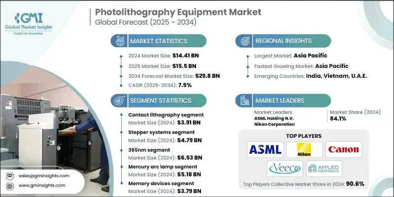
全球对智慧型手机、资料中心、人工智慧处理器和汽车电子产品中使用的更小、更快、更节能的晶片的需求激增,推动了对尖端光刻设备的投资,特别是针对 7nm 以下节点的投资。
| 市场范围 | |
|---|---|
| 起始年份 | 2024 |
| 预测年份 | 2025-2034 |
| 起始值 | 144.1亿美元 |
| 预测值 | 298亿美元 |
| 复合年增长率 | 7.5% |
接触式光刻技术需求不断成长
2024年,接触式微影技术占据了相当大的份额,这主要得益于半导体和微加工应用,尤其是在高产量和低成本优先于极高解析度的应用领域。虽然接触式微影技术不如更先进的光刻方法精确,但它广泛应用于MEMS生产、印刷电路板(PCB)和某些化合物半导体製程。
步进系统的应用日益广泛
步进式系统在2024年占据了相当大的市场。这些系统每次曝光一个晶片,提供精确的对准和套刻控制,这对于模拟、射频和功率装置中使用的成熟製程技术至关重要。儘管EUV技术正在兴起,但步进式系统由于其价格实惠、可靠性高,在传统和特殊晶圆厂中仍然需求旺盛。
储存设备将获得发展动力
2024年,储存设备市场将占据相当大的份额,这得益于对更高密度和更快性能的需求,从而推动了对能够处理日益复杂图案的先进光刻设备的需求。 DRAM 和 NAND 快闪记忆体製造商依靠 DUV 和 EUV 系统来突破微缩极限,并实现 3D NAND 和 DDR5 等创新。
亚太地区将成为利润丰厚的地区
2025年至2034年期间,亚太地区光刻设备市场将以可观的复合年增长率成长,这得益于台湾、韩国、中国大陆和日本等半导体製造强国的崛起。这些国家拥有全球最大的晶圆代工厂和记忆体生产商,使该地区成为先进和传统节点製造的关键枢纽。
光刻设备市场的主要参与者有 Gigaphoton Inc.、佳能公司、滨松光子株式会社、Veeco Instruments Inc.、EV Group (EVG)、SCREEN Semiconductor Solutions Co., Ltd.、日立高科技公司、ASML Holding NV、Xenics NVec、应用材料公司、KLA Corporation、日立高科技公司、ASML Holding NV、Xenics NVS、应用程式材料公司、KLA Corporation、Cymer LLC、S VMLA Corporation、VMLA Corporation、BMLA Corporation、Cyberim 所有Inc.。
为了巩固其在光刻设备市场的地位,各公司正在实施以创新、可扩展性和区域扩张为重点的策略。领先的公司正在大力投资下一代技术,例如高数值孔径 EUV 和先进的光学系统,以保持其技术优势。同时,他们正在丰富其产品线,以满足尖端和传统晶圆厂的需求,确保在整个晶片生产过程中保持相关性。
目录
第一章:方法论与范围
第 2 章:执行摘要
第三章:行业洞察
- 产业生态系统分析
- 供应商格局
- 利润率
- 成本结构
- 每个阶段的增值
- 影响价值链的因素
- 中断
- 产业衝击力
- 成长动力
- 先进节点半导体需求激增
- 全球半导体代工产能快速扩张
- 人工智慧、物联网和汽车电子产品的采用加速
- 向高NA EUV光刻技术过渡
- 政府主导的半导体计划和补贴
- 产业陷阱与挑战
- EUV系统成本极高,且复杂度极高
- 全球出口限制和地缘政治紧张局势
- 市场机会
- 新兴地区半导体工厂的扩张
- 人工智慧和机器学习在光刻製程控制中的集成
- 高数值孔径EUV技术的发展
- 对先进封装和 3D IC 的需求不断增长
- 成长动力
- 成长潜力分析
- 监管格局
- 北美洲
- 欧洲
- 亚太地区
- 拉丁美洲
- 中东和非洲
- 波特的分析
- PESTEL分析
- 技术和创新格局
- 当前的技术趋势
- 新兴技术
- 价格趋势
- 按地区
- 按产品
- 定价策略
- 新兴商业模式
- 合规性要求
- 永续性措施
- 消费者情绪分析
- 专利和智慧财产权分析
- 地缘政治与贸易动态
第四章:竞争格局
- 公司介绍市占率分析
- 公司市占率分析
- 按地区
- 北美洲
- 欧洲
- 亚太地区
- 市场集中度分析
- 关键参与者的竞争基准
- 财务绩效比较
- 收入
- 利润率
- 研发
- 产品组合比较
- 产品范围广度
- 科技
- 创新
- 地理位置比较
- 全球足迹分析
- 服务网路覆盖
- 各地区市场渗透率
- 竞争定位矩阵
- 领导者
- 挑战者
- 追踪者
- 利基市场参与者
- 战略展望矩阵
- 财务绩效比较
- 2021-2024 年关键发展
- 併购
- 伙伴关係与合作
- 技术进步
- 扩张和投资策略
- 永续发展倡议
- 数位转型倡议
- 新兴/新创企业竞争对手格局
第五章:市场估计与预测:依技术类型,2021 - 2034
- 接触光刻
- 接近式光刻
- 投影光刻
- 奈米压印光刻
- 电子束(E-beam)光刻
- 极紫外线(EUV)光刻
- 其他的
第六章:市场估计与预测:按设备类型,2021 - 2034 年
- 步进系统
- 扫描器系统
- 轨道系统
- 计量和检测工具
- 掩模对准器
- 其他的
第七章:市场估计与预测:按光源,2021 - 2034 年
- 汞弧灯
- 准分子雷射
- 氟化氪(KrF)
- 氟化氩(ArF)
- 雷射产生的等离子体(LPP - 用于 EUV)
第 8 章:市场估计与预测:按应用,2021 - 2034 年
- 储存装置
- 逻辑积体电路
- 铸造厂(合约製造)
- IDM(整合设备製造商)
- 类比和混合讯号积体电路
- MEMS和感测器製造
- 先进封装(2.5D/3D IC)
- 显示面板(LCD、OLED)
第九章:市场估计与预测:按地区,2021 - 2034
- 主要趋势
- 北美洲
- 我们
- 加拿大
- 欧洲
- 德国
- 英国
- 法国
- 义大利
- 西班牙
- 荷兰
- 鱼子
- 亚太地区
- 中国
- 印度
- 日本
- 韩国
- 澳洲
- 亚太区
- 拉丁美洲
- 巴西
- 墨西哥
- 阿根廷
- 罗拉塔姆
- 中东和非洲
- 阿联酋
- 沙乌地阿拉伯
- 南非
- 罗马
第十章:公司简介
- Applied Materials, Inc.
- ASML Holding NV
- Canon Inc.
- Cymer LLC (ASML subsidiary)
- DAIHEN Corporation
- EV Group (EVG)
- Gigaphoton Inc.
- Hamamatsu Photonics KK
- Hitachi High-Tech Corporation
- HOYA Corporation
- JEOL Ltd.
- KLA Corporation
- Lam Research Corporation
- Nikon Corporation
- Nova Ltd.
- Onto Innovation Inc.
- Photronics, Inc.
- SCREEN Semiconductor Solutions Co., Ltd.
- SUSS MicroTec SE
- Tokyo Electron Limited (TEL)
- Toppan Photomasks, Inc.
- Toray Industries, Inc.
- Ushio Inc.
- Veeco Instruments Inc.
- Xenics NV
The Global Photolithography Equipment Market was valued at USD 14.41 billion in 2024 and is estimated to grow at a CAGR of 7.5% to reach USD 29.8 billion by 2034.
The global surge in demand for smaller, faster, and more energy-efficient chips used in smartphones, data centers, AI processors, and automotive electronics is fueling investment in cutting-edge photolithography equipment, particularly for nodes below 7nm.
| Market Scope | |
|---|---|
| Start Year | 2024 |
| Forecast Year | 2025-2034 |
| Start Value | $14.41 Billion |
| Forecast Value | $29.8 Billion |
| CAGR | 7.5% |
Rising Demand for Contact Lithography
The contact lithography segment held a significant share in 2024, driven by semiconductor and microfabrication applications, particularly where high throughput and lower costs are prioritized over extreme resolution. While it lacks the precision of more advanced lithography methods, contact lithography is widely used in MEMS production, printed circuit boards (PCBs), and certain compound semiconductor processes.
Increasing Adoption of Stepper Systems
The stepper systems segment generated a substantial share in 2024. These systems expose one die at a time, providing precise alignment and overlay control, which is critical for mature process technologies used in analog, RF, and power devices. Despite the rise of EUV, steppers remain in strong demand due to their affordability and reliability across legacy and specialty fabs.
Memory Devices to Gain Traction
The memory devices segment held a sizeable share in 2024, driven by the need for higher density and faster performance, which is driving demand for advanced photolithography equipment capable of handling increasingly complex patterns. DRAM and NAND flash manufacturers rely on both DUV and EUV systems to push scaling limits and enable innovations such as 3D NAND and DDR5.
Asia Pacific to Emerge as a Lucrative Region
Asia Pacific photolithography equipment market will grow at a decent CAGR during 2025-2034, driven by the presence of semiconductor manufacturing powerhouses such as Taiwan, South Korea, China, and Japan. These countries host the world's largest foundries and memory producers, making the region a critical hub for both advanced and legacy node manufacturing.
Major players in the photolithography equipment market are Gigaphoton Inc., Canon Inc., Hamamatsu Photonics K.K., Veeco Instruments Inc., EV Group (EVG), SCREEN Semiconductor Solutions Co., Ltd., Hitachi High-Tech Corporation, ASML Holding N.V., Xenics NV, Applied Materials, Inc., KLA Corporation, Cymer LLC, SUSS MicroTec SE, Nikon Corporation, Ushio Inc., Lam Research Corporation, and Onto Innovation Inc.
To solidify their position in the photolithography equipment market, companies are executing strategies focused on innovation, scalability, and regional expansion. Leading firms are investing heavily in next-generation technologies such as high-NA EUV and advanced optical systems to maintain their technological edge. At the same time, they are diversifying their offerings to cater to both leading-edge and legacy fabs, ensuring relevance across the full spectrum of chip production.
Table of Contents
Chapter 1 Methodology and Scope
- 1.1 Market scope and definition
- 1.2 Research design
- 1.2.1 Research approach
- 1.2.2 Data collection methods
- 1.3 Data mining sources
- 1.3.1 Global
- 1.3.2 Regional/Country
- 1.4 Base estimates and calculations
- 1.4.1 Base year calculation
- 1.4.2 Key trends for market estimation
- 1.5 Primary research and validation
- 1.5.1 Primary sources
- 1.6 Forecast model
- 1.7 Research assumptions and limitations
Chapter 2 Executive Summary
- 2.1 Industry 3600 synopsis
- 2.2 Key market trends
- 2.2.1. Technology type
- 2.2.2 Equipment type
- 2.2.3 Wavelength
- 2.2.4 Light source
- 2.2.5 Application
- 2.2.6 North America
- 2.2.7 Europe
- 2.2.8 Asia Pacific
- 2.2.9 Latin America
- 2.2.10 Middle East & Africa
- 2.3 TAM Analysis, 2025-2034 (USD Million)
- 2.4 CXO perspectives: Strategic imperatives
- 2.5 Executive decision points
- 2.6 Critical success factors
- 2.7 Future outlook and strategic recommendations
Chapter 3 Industry Insights
- 3.1 Industry ecosystem analysis
- 3.1.1 Supplier landscape
- 3.1.2 Profit margin
- 3.1.3 Cost structure
- 3.1.4 Value addition at each stage
- 3.1.5 Factor affecting the value chain
- 3.1.6 Disruptions
- 3.2 Industry impact forces
- 3.2.1 Growth drivers
- 3.2.1.1 Surging demand for advanced-node semiconductors
- 3.2.1.2 Rapid expansion of global semiconductor foundry capacity
- 3.2.1.3 Acceleration in AI, IoT, and automotive electronics adoption
- 3.2.1.4 Transition toward High-NA EUV lithography
- 3.2.1.5 Government-led semiconductor initiatives and subsidies
- 3.2.2 Industry pitfalls and challenges
- 3.2.2.1 Extremely high cost and complexity of EUV systems
- 3.2.2.2 Global export restrictions and geopolitical tensions
- 3.2.3 Market opportunities
- 3.2.3.1 Expansion of semiconductor fabs in emerging regions
- 3.2.3.2 Integration of AI and machine learning in lithography process control
- 3.2.3.3 Development of High-NA EUV technology
- 3.2.3.4 Growing demand for advanced packaging and 3D ICs
- 3.2.1 Growth drivers
- 3.3 Growth potential analysis
- 3.4 Regulatory landscape
- 3.4.1 North America
- 3.4.2 Europe
- 3.4.3 Asia Pacific
- 3.4.4 Latin America
- 3.4.5 Middle East & Africa
- 3.5 Porter’s analysis
- 3.6 PESTEL analysis
- 3.7 Technological and innovation landscape
- 3.7.1 Current technological trends
- 3.7.2 Emerging technologies
- 3.8 Price trends
- 3.8.1 By region
- 3.8.2 By product
- 3.9 Pricing strategies
- 3.10 Emerging business models
- 3.11 Compliance requirements
- 3.12 Sustainability measures
- 3.13 Consumer sentiment analysis
- 3.14 Patent and IP analysis
- 3.15 Geopolitical and trade dynamics
Chapter 4 Competitive Landscape, 2024
- 4.1 Introduction company market share analysis
- 4.2 Company market share analysis
- 4.2.1 By region
- 4.2.1. North America
- 4.2.2. Europe
- 4.2.3. Asia Pacific
- 4.2.2 Market concentration analysis
- 4.3 Competitive benchmarking of key players
- 4.3.1 Financial performance comparison
- 4.3.1.1. Revenue
- 4.3.1.2. Profit margin
- 4.3.1.3. R&D
- 4.3.2 Product portfolio comparison
- 4.3.2.1. Product range breadth
- 4.3.2.2. Technology
- 4.3.2.3. Innovation
- 4.3.3 Geographic presence comparison
- 4.3.3.1. Global footprint analysis
- 4.3.3.2. Service network coverage
- 4.3.3.3. Market penetration by region
- 4.3.4 Competitive positioning matrix
- 4.3.4.1. Leaders
- 4.3.4.2. Challengers
- 4.3.4.3. Followers
- 4.3.4.4. Niche players
- 4.3.5 Strategic outlook matrix
- 4.3.1 Financial performance comparison
- 4.4 Key developments, 2021-2024
- 4.4.1 Mergers and acquisitions
- 4.4.2 Partnerships and collaborations
- 4.4.3 Technological advancements
- 4.4.4 Expansion and investment strategies
- 4.4.5 Sustainability initiatives
- 4.4.6 Digital transformation initiatives
- 4.5 Emerging/ startup competitors landscape
Chapter 5 Market Estimates & Forecast, By Technology Type, 2021 - 2034 (USD Million)
- 5.1 Contact lithography
- 5.2 Proximity lithography
- 5.3 Projection lithography
- 5.4 Nanoimprint lithography
- 5.5 Electron beam (E-beam) lithography
- 5.6 Extreme ultraviolet (EUV) lithography
- 5.7 Others
Chapter 6 Market estimates & forecast, By Equipment Type, 2021 - 2034 (USD Million)
- 6.1 Stepper systems
- 6.2 Scanner systems
- 6.3 Track systems
- 6.4 Metrology & inspection tools
- 6.5 Mask aligners
- 6.6 Others
Chapter 7 Market estimates & forecast, By Light Source, 2021 - 2034 (USD Million)
- 7.1 Mercury arc lamp
- 7.2 Excimer laser
- 7.3 Krypton fluoride (KrF)
- 7.4 Argon fluoride (ArF)
- 7.5 Laser-produced plasma (LPP - for EUV)
Chapter 8 Market Estimates and Forecast, By Application, 2021 - 2034 ( USD Million)
- 8.1 Memory devices
- 8.2 Logic ICs
- 8.3 Foundry (Contract manufacturing)
- 8.4 IDMs (Integrated Device Manufacturers)
- 8.5 Analog & mixed signal ICs
- 8.6 MEMS & sensor fabrication
- 8.7 Advanced packaging (2.5D / 3D ICs)
- 8.8 Display panels (LCD, OLED)
Chapter 9 Market Estimates and Forecast, By Region, 2021 - 2034 (USD Million)
- 9.1 Key trends
- 9.2 North America
- 9.2.1 U.S.
- 9.2.2 Canada
- 9.3 Europe
- 9.3.1 Germany
- 9.3.2 U.K.
- 9.3.3 France
- 9.3.4 Italy
- 9.3.5 Spain
- 9.3.6 Netherlands
- 9.3.7 ROE
- 9.4 Asia Pacific
- 9.4.1 China
- 9.4.2 India
- 9.4.3 Japan
- 9.4.4 South Korea
- 9.4.5 Australia
- 9.4.6 RoAPAC
- 9.5 Latin America
- 9.5.1 Brazil
- 9.5.2 Mexico
- 9.5.3 Argentina
- 9.5.4 RoLATAM
- 9.6 Middle East & Africa
- 9.6.1 UAE
- 9.6.2 Saudi Arabia
- 9.6.3 South Africa
- 9.6.4 RoMEA
Chapter 10 Company Profile
- 10.1 Applied Materials, Inc.
- 10.2 ASML Holding N.V.
- 10.3 Canon Inc.
- 10.4 Cymer LLC (ASML subsidiary)
- 10.5 DAIHEN Corporation
- 10.6 EV Group (EVG)
- 10.7 Gigaphoton Inc.
- 10.8 Hamamatsu Photonics K.K.
- 10.9 Hitachi High-Tech Corporation
- 10.10 HOYA Corporation
- 10.11 JEOL Ltd.
- 10.12 KLA Corporation
- 10.13 Lam Research Corporation
- 10.14 Nikon Corporation
- 10.15 Nova Ltd.
- 10.16 Onto Innovation Inc.
- 10.17 Photronics, Inc.
- 10.18 SCREEN Semiconductor Solutions Co., Ltd.
- 10.19 SUSS MicroTec SE
- 10.20 Tokyo Electron Limited (TEL)
- 10.21 Toppan Photomasks, Inc.
- 10.22 Toray Industries, Inc.
- 10.23 Ushio Inc.
- 10.24 Veeco Instruments Inc.
- 10.25 Xenics NV
 微影术设备市场:2026-2032年全球市场预测(依产品类型、部署模式、波长、客户类型和应用划分)
 2026年全球微影术设备市场报告2026年全球半导体对准器市场报告
 微影术设备市场-全球产业规模、份额、趋势、机会和预测:按类型、深紫外线类型、波长、装置波长、最终用途、应用、地区和竞争格局划分,2021-2031年193nm准分子雷射市场:按雷射类型、功率输出、销售管道和应用划分 - 全球预测(2026-2032)
 光刻设备市场规模、份额、趋势及预测(按製程、波长、设备波长、应用、最终用途和地区),2025 年至 2033 年
 半导体微影术设备市场:未来预测(2025-2030)
 光刻设备市场,按工艺、按光源、按波长、按最终用户、按国家和地区 - 2024-2032 年行业分析、市场规模、市场份额和预测