


 |
市场调查报告书
商品编码
1959280
先进半导体封装市场机会、成长要素、产业趋势分析及2026年至2035年预测Advanced Semiconductor Packaging Market Opportunity, Growth Drivers, Industry Trend Analysis, and Forecast 2026 - 2035 |
||||||
2025年全球先进半导体封装市场价值为335亿美元,预计2035年将达953亿美元,年复合成长率为11%。
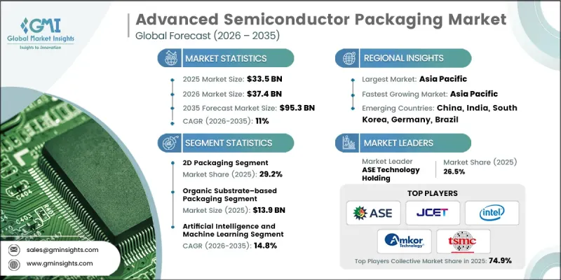
市场扩张的驱动力主要来自晶片级处理器架构的加速发展以及下一代无线基础设施的广泛部署。这些趋势正在加速对高密度射频整合技术和系统级封装)配置的需求,以支援紧凑型高性能电子设备。同时,先进製程节点不断上涨的製造成本和产量比率,使得业界更加重视先进封装技术,将其视为提升效能和成本效益的关键驱动因素。此外,人工智慧加速器日益普及,需要高频宽记忆体集成,这也进一步推动了市场需求,因为这些配置能够实现高吞吐量,满足高要求的运算工作负载的需求。同时,超大规模资料中心和高效能运算平台的扩展也推动了2.5D和3D积体电路架构的应用。这些封装创新实现了异质整合、更高的互连密度和更强的能源效率,进一步提升了它们在下一代半导体设计中的战略重要性。
| 市场范围 | |
|---|---|
| 开始年份 | 2025 |
| 预测年份 | 2026-2035 |
| 起始值 | 335亿美元 |
| 预测金额 | 953亿美元 |
| 复合年增长率 | 11% |
2025年,二维封装仍维持其最大市场份额,达29.2%。其持续领先地位得益于成熟逻辑节点、类比元件、电源管理元件和混合讯号积体电路的高使用率。由于成本稳定、製造可靠性高且产量比率优化,这种封装形式对大规模生产仍然极具吸引力。家用电子电器、汽车系统和工业自动化等关键终端用户产业继续依赖二维封装,以实现与现有製造流程和稳健供应链的无缝整合。其扩充性和久经考验的可靠性确保了在大批量生产环境中的持续需求。
预计到2025年,基于有机基板的封装市场规模将达到139亿美元。该领域的成长主要得益于覆晶封装和先进多层封装设计在处理器、连接组件和汽车电子产品中的广泛应用。有机基板兼具优异的电气性能、机械柔软性和成本效益,使其成为高输入/输出密度应用的理想选择。成熟的生产生态系统和持续的材料创新进一步推动了该领域的成长。在消费性电子设备、通讯基础设施和工业系统等领域,对性能稳定性和大规模生产能力的需求仍然强劲。
预计到2025年,北美先进半导体封装市场占有率将达到22.8%。在人工智慧处理器和先进资料中心晶片需求不断增长的推动下,该地区的发展正在加速。由整合装置製造商和外包半导体组装测试服务商组成的强大生态系统,为先进封装技术的快速普及提供了有力支援。 2.5D和3D整合策略的日益普及,使区域内企业能够克服传统平面架构在效能、频宽和功耗方面的限制。对半导体研发、本土製造能力和先进运算基础设施的持续投入,进一步巩固了北美在全球市场的竞争优势。
目录
第一章:调查方法和范围
第二章执行摘要
第三章业界考察
- 生态系分析
- 供应商情况
- 利润率
- 成本结构
- 每个阶段增加的价值
- 影响价值链的因素
- 中断
- 影响产业的因素
- 促进因素
- 需要高频宽记忆体整合的AI加速器
- 高效能运算和资料中心采用 2.5D 和 3D 积体电路
- Chiplet架构取代了单晶片SoC设计
- 需要高密度射频封装的5G基地台
- 先进节点的成本推高了封装创新的价值。
- 产业潜在风险与挑战
- 对先进包装工厂的高资本投入
- 高功率封装元件温度控管的复杂性
- 市场机会
- 透过代工厂与OSAT厂商的伙伴关係,扩大先进封装产能。
- 用于下一代资料中心互连的联合封装光元件
- 促进因素
- 成长潜力分析
- 监理情势
- 波特五力分析
- PESTEL 分析
- 科技与创新趋势
- 当前技术趋势
- 新兴技术
- 价格趋势
- 按地区
- 副产品
- 定价策略
- 新兴经营模式
- 合规要求
- 专利和智慧财产权分析
- 地缘政治和贸易趋势
第四章 竞争情势
- 介绍
- 企业市占率分析
- 按地区
- 市场集中度分析
- 主要企业的竞争标竿分析
- 财务绩效比较
- 收入
- 利润率
- 研究与开发
- 产品系列比较
- 产品线广度
- 科技
- 创新
- 地理位置比较
- 全球扩张分析
- 服务网路覆盖
- 按地区分類的市场渗透率
- 竞争定位矩阵
- 领导企业
- 受让人
- 追踪者
- 小众玩家
- 战略展望矩阵
- 财务绩效比较
- 主要进展
- 併购
- 伙伴关係与合作
- 技术进步
- 扩张和投资策略
- 数位转型计划
- 新兴/Start-Ups竞争对手的发展趋势
第五章 市场估价与预测:依包装架构划分,2022-2035年
- 二维封装(单晶粒,单平面)
- 2.5D封装(多晶片、基于中介层的单垂直平面)
- 3D封装(垂直晶粒堆迭)
- 基于TSV的3D封装
- 基于混合键结的3D包装
- 晶圆层次电子构装(WLP)
- 扇入晶圆层次电子构装(FI-WLP)
- 扇出型晶圆层次电子构装(FO-WLP)
- 混合/多架构封装
第六章 市场估价与预测:依包装材料划分,2022-2035年
- 基于有机基板的包装
- 基于硅中介层的封装
- 基于RDL(重构晶圆)的封装
- 3D堆迭是主流封装方法(晶粒间连接材料平台)。
- 基于玻璃中介层的封装
第七章 市场估计与预测:依应用领域划分,2022-2035年
- 人工智慧和机器学习
- 高效能运算 (HPC) 和资料中心
- 行动通讯
- 车
- 家用电子电器
- 工业、航太和国防领域。
第八章 市场估计与预测:依地区划分,2022-2035年
- 北美洲
- 我们
- 加拿大
- 欧洲
- 德国
- 英国
- 法国
- 西班牙
- 义大利
- 俄罗斯
- 亚太地区
- 中国
- 印度
- 日本
- 澳洲
- 韩国
- 拉丁美洲
- 巴西
- 墨西哥
- 阿根廷
- 中东和非洲
- 南非
- 沙乌地阿拉伯
- 阿拉伯聯合大公国
第九章:公司简介
- 主要企业
- ASE Technology Holding
- Amkor Technology, Inc.
- Taiwan Semiconductor Manufacturing Company(TSMC)
- Samsung Electronics
- Intel Corporation
- 按地区分類的主要企业
- 北美洲
- GlobalFoundries Inc.
- Texas Instruments
- Micron Technology, Inc.
- 亚太地区
- JCET Group Co., Ltd.
- Powertech Technology Inc.(PTI)
- Huatian Technology Co., Ltd.
- Tongfu Microelectronics Co., Ltd.
- ChipMOS Technologies Inc.
- UTAC Holdings Ltd.
- HANA Micron Inc.
- SK hynix
- 北美洲
- 特殊玩家/干扰者
- China Wafer Level CSP Co., Ltd.(CWLP)
The Global Advanced Semiconductor Packaging Market was valued at USD 33.5 billion in 2025 and is estimated to grow at a CAGR of 11% to reach USD 95.3 billion by 2035.
Market expansion is fueled by the increasing transition toward chiplet-based processor architectures and the widespread deployment of next-generation wireless infrastructure. These trends are accelerating demand for high-density radio frequency integration and system-in-package configurations that support compact, high-performance electronics. At the same time, escalating fabrication costs and yield constraints at leading-edge process nodes are shifting industry focus toward advanced packaging as a critical driver of performance gains and cost efficiency. The growing adoption of AI accelerators that require high-bandwidth memory integration is further strengthening demand, as these configurations enable extremely high data throughput essential for advanced computing workloads. In addition, expansion of hyperscale data centers and high-performance computing platforms is driving the implementation of 2.5D and 3D integrated circuit architectures. These packaging innovations enable heterogeneous integration, improved interconnect density, and enhanced power efficiency, reinforcing their strategic importance in next-generation semiconductor design.
| Market Scope | |
|---|---|
| Start Year | 2025 |
| Forecast Year | 2026-2035 |
| Start Value | $33.5 Billion |
| Forecast Value | $95.3 Billion |
| CAGR | 11% |
In 2025, the 2D packaging segment accounted for 29.2% share, maintaining the largest share. Its continued dominance is supported by strong utilization across mature logic nodes, analog components, power management devices, and mixed-signal integrated circuits. This packaging format remains highly attractive for large-scale production due to its cost stability, manufacturing reliability, and optimized yield performance. Key end-use industries, including consumer electronics, automotive systems, and industrial automation, continue to depend on 2D packaging because it aligns seamlessly with established fabrication processes and resilient supply networks. Its scalability and proven reliability ensure consistent demand across high-volume production environments.
The organic substrate-based packaging segment reached USD 13.9 billion in 2025. Growth in this category is driven by widespread deployment in flip-chip assemblies and advanced laminate package designs used in processors, connectivity components, and automotive electronics. Organic substrates provide an optimal combination of electrical performance, mechanical flexibility, and cost efficiency, making them well-suited for applications requiring high input/output density. Established production ecosystems and continuous material innovation further reinforce segment growth. Demand remains strong across consumer devices, communications infrastructure, and industrial systems, where performance consistency and manufacturability at scale are essential.
North America Advanced Semiconductor Packaging Market held a 22.8% share in 2025. The region is experiencing accelerated development driven by rising demand for AI-enabled processors and advanced data center chips. A robust ecosystem of integrated device manufacturers and outsourced semiconductor assembly and test providers supports rapid adoption of advanced packaging technologies. Increasing implementation of 2.5D and 3D integration strategies is helping regional players overcome performance, bandwidth, and power limitations associated with conventional planar architectures. Continued investment in semiconductor research, domestic manufacturing capabilities, and advanced computing infrastructure is further strengthening North America's competitive position in the global market.
Key companies operating in the Global Advanced Semiconductor Packaging Market include Taiwan Semiconductor Manufacturing Company (TSMC), Samsung Electronics, Intel Corporation, Amkor Technology, Inc., ASE Technology Holding, JCET Group Co., Ltd., Powertech Technology Inc. (PTI), GlobalFoundries Inc., Micron Technology, Inc., SK hynix, Texas Instruments, Tongfu Microelectronics Co., Ltd., Huatian Technology Co., Ltd., ChipMOS Technologies Inc., HANA Micron Inc., China Wafer Level CSP Co., Ltd. (CWLP), and UTAC Holdings Ltd. Companies in the Advanced Semiconductor Packaging Market are reinforcing their market position through strategic investments in research and development focused on high-density interconnect technologies and advanced substrate materials. Many players are expanding manufacturing capacity to meet rising demand from AI, high-performance computing, and automotive electronics sectors. Collaborative partnerships with foundries, memory manufacturers, and system designers are enabling co-optimization of chip architecture and packaging solutions. Firms are also prioritizing vertical integration to improve supply chain resilience and reduce production bottlenecks.
Table of Contents
Chapter 1 Methodology and Scope
- 1.1 Market scope and definition
- 1.2 Research design
- 1.2.1 Research approach
- 1.2.2 Data collection methods
- 1.3 Data mining sources
- 1.3.1 Global
- 1.3.2 Regional/Country
- 1.4 Base estimates and calculations
- 1.4.1 Base year calculation
- 1.4.2 Key trends for market estimation
- 1.5 Primary research and validation
- 1.5.1 Primary sources
- 1.6 Forecast model
- 1.7 Research assumptions and limitations
Chapter 2 Executive Summary
- 2.1 Industry 360° synopsis, 2022 - 2035
- 2.2 Key market trends
- 2.2.1 Packaging architecture trends
- 2.2.2 Packaging material trends
- 2.2.3 Application trends
- 2.2.4 Regional trends
- 2.3 TAM Analysis, 2026-2035
- 2.4 CXO perspectives: Strategic imperatives
- 2.4.1 Executive decision points
- 2.4.2 critical success factors
- 2.5 Future outlook and strategic recommendations
Chapter 3 Industry Insights
- 3.1 Industry ecosystem analysis
- 3.1.1 Supplier Landscape
- 3.1.2 Profit Margin
- 3.1.3 Cost structure
- 3.1.4 Value addition at each stage
- 3.1.5 Factor affecting the value chain
- 3.1.6 Disruptions
- 3.2 Industry impact forces
- 3.2.1 Growth drivers
- 3.2.1.1 AI accelerators demanding high-bandwidth memory integration
- 3.2.1.2 HPC and data centers adopting 2.5D and 3D ICs
- 3.2.1.3 Chiplet architectures replacing monolithic SoC designs
- 3.2.1.4 5G base stations requiring high-density RF packaging
- 3.2.1.5 Advanced nodes cost pushing value toward packaging innovation
- 3.2.2 Industry pitfalls and challenges
- 3.2.2.1 High capital expenditure for advanced packaging fabs
- 3.2.2.2 Thermal management complexity in high-power packaged devices
- 3.2.3 Market opportunities
- 3.2.3.1 Foundry-OSAT partnerships for advanced packaging capacity expansion
- 3.2.3.2 Co-packaged optics enabling next-generation data center interconnects
- 3.2.1 Growth drivers
- 3.3 Growth potential analysis
- 3.4 Regulatory landscape
- 3.4.1 North America
- 3.4.2 Europe
- 3.4.3 Asia Pacific
- 3.4.4 Latin America
- 3.4.5 Middle East & Africa
- 3.5 Porter's analysis
- 3.6 PESTEL analysis
- 3.7 Technology and Innovation landscape
- 3.7.1 Current technological trends
- 3.7.2 Emerging technologies
- 3.8 Price trends
- 3.8.1 By region
- 3.8.2 By product
- 3.9 Pricing Strategies
- 3.10 Emerging Business Models
- 3.11 Compliance Requirements
- 3.12 Patent and IP analysis
- 3.13 Geopolitical and trade dynamics
Chapter 4 Competitive Landscape, 2025
- 4.1 Introduction
- 4.2 Company market share analysis
- 4.2.1 By region
- 4.2.1.1 North America
- 4.2.1.2 Europe
- 4.2.1.3 Asia Pacific
- 4.2.1.4 Latin America
- 4.2.1.5 Middle East & Africa
- 4.2.2 Market concentration analysis
- 4.2.1 By region
- 4.3 Competitive benchmarking of key players
- 4.3.1 Financial performance comparison
- 4.3.1.1 Revenue
- 4.3.1.2 Profit margin
- 4.3.1.3 R&D
- 4.3.2 Product portfolio comparison
- 4.3.2.1 Product range breadth
- 4.3.2.2 Technology
- 4.3.2.3 Innovation
- 4.3.3 Geographic presence comparison
- 4.3.3.1 Global footprint analysis
- 4.3.3.2 Service network coverage
- 4.3.3.3 Market penetration by region
- 4.3.4 Competitive positioning matrix
- 4.3.4.1 Leaders
- 4.3.4.2 Challengers
- 4.3.4.3 Followers
- 4.3.4.4 Niche players
- 4.3.5 Strategic outlook matrix
- 4.3.1 Financial performance comparison
- 4.4 Key developments
- 4.4.1 Mergers and acquisitions
- 4.4.2 Partnerships and collaborations
- 4.4.3 Technological advancements
- 4.4.4 Expansion and investment strategies
- 4.4.5 Digital transformation initiatives
- 4.5 Emerging/ startup competitors landscape
Chapter 5 Market Estimates and Forecast, By Packaging Architecture, 2022 - 2035 (USD Million)
- 5.1 Key trends
- 5.2 2D Packaging (single-die, single-plane)
- 5.3 2.5D Packaging (multi-die, interposer-based, single vertical plane)
- 5.4 3D Packaging (Vertical Die Stacking)
- 5.4.1 TSV-based 3D packaging
- 5.4.2 Hybrid bonding-based 3D packaging
- 5.5 Wafer-level packaging (WLP)
- 5.5.1 Fan-in wafer-level packaging (FI-WLP)
- 5.5.2 Fan-out wafer-level packaging (FO-WLP)
- 5.6 Hybrid/multi-architecture packaging
Chapter 6 Market Estimates and Forecast, By Packaging Material, 2022 - 2035 (USD Million)
- 6.1 Key trends
- 6.2 Organic substrate-based packaging
- 6.3 Silicon interposer-based packaging
- 6.4 RDL-based (reconstituted wafer) packaging
- 6.5 3D stack-dominant packaging (die-to-die material platform)
- 6.6 Glass interposer-based packaging
Chapter 7 Market Estimates and Forecast, By Application, 2022 - 2035 (USD Million)
- 7.1 Key trends
- 7.2 Artificial intelligence and machine learning
- 7.3 High-performance computing (HPC) and data center
- 7.4 Mobile and communications
- 7.5 Automotive
- 7.6 Consumer electronics
- 7.7 Industrial, aerospace and defense
Chapter 8 Market Estimates and Forecast, By Region, 2022 - 2035 (USD Million)
- 8.1 Key trends
- 8.2 North America
- 8.2.1 U.S.
- 8.2.2 Canada
- 8.3 Europe
- 8.3.1 Germany
- 8.3.2 UK
- 8.3.3 France
- 8.3.4 Spain
- 8.3.5 Italy
- 8.3.6 Russia
- 8.4 Asia Pacific
- 8.4.1 China
- 8.4.2 India
- 8.4.3 Japan
- 8.4.4 Australia
- 8.4.5 South Korea
- 8.5 Latin America
- 8.5.1 Brazil
- 8.5.2 Mexico
- 8.5.3 Argentina
- 8.6 Middle East and Africa
- 8.6.1 South Africa
- 8.6.2 Saudi Arabia
- 8.6.3 UAE
Chapter 9 Company Profiles
- 9.1 Global Key Players
- 9.1.1 ASE Technology Holding
- 9.1.2 Amkor Technology, Inc.
- 9.1.3 Taiwan Semiconductor Manufacturing Company (TSMC)
- 9.1.4 Samsung Electronics
- 9.1.5 Intel Corporation
- 9.2 Regional key players
- 9.2.1 North America
- 9.2.1.1 GlobalFoundries Inc.
- 9.2.1.2 Texas Instruments
- 9.2.1.3 Micron Technology, Inc.
- 9.2.2 Asia Pacific
- 9.2.2.1 JCET Group Co., Ltd.
- 9.2.2.2 Powertech Technology Inc. (PTI)
- 9.2.2.3 Huatian Technology Co., Ltd.
- 9.2.2.4 Tongfu Microelectronics Co., Ltd.
- 9.2.2.5 ChipMOS Technologies Inc.
- 9.2.2.6 UTAC Holdings Ltd.
- 9.2.2.7 HANA Micron Inc.
- 9.2.2.8 SK hynix
- 9.2.1 North America
- 9.3 Niche Players/Disruptors
- 9.3.1 China Wafer Level CSP Co., Ltd. (CWLP)


