


 |
市场调查报告书
商品编码
1959568
2026 年至 2035 年电子束晶圆检测系统市场的机会、成长要素、产业趋势分析与预测。E-Beam Wafer Inspection System Market Opportunity, Growth Drivers, Industry Trend Analysis, and Forecast 2026 - 2035 |
||||||
2025 年全球电子束晶圆检测系统市值为 14 亿美元,预计到 2035 年将达到 69 亿美元,复合年增长率为 18.3%。
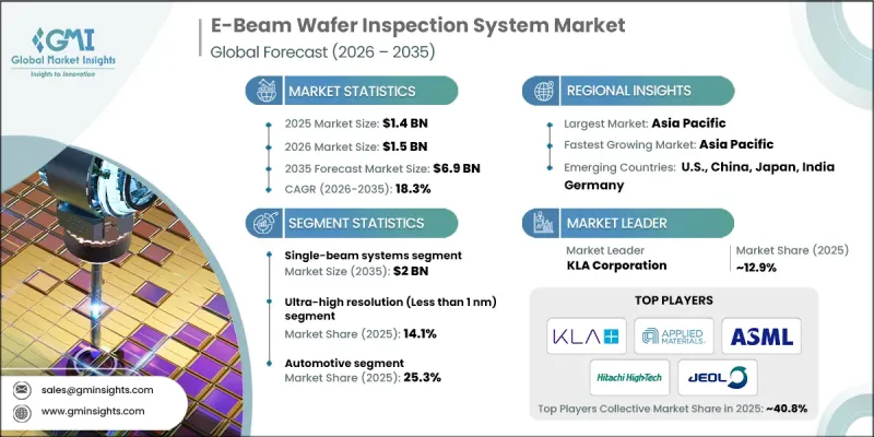
半导体製造产能投资的增加以及先进元件日益复杂化是推动市场成长的主要因素。製造商正在将人工智慧 (AI) 和机器学习 (ML) 演算法整合到其检测系统中,以提高缺陷检测率和产量比率。新兴技术的蓬勃发展,例如 5G、人工智慧、物联网 (IoT) 和汽车电子等,对高品质晶圆的需求日益增长,也推动了市场需求。随着晶圆结构变得越来越复杂,对精密检测工具的需求也不断增加,尤其是在家用电子电器、通讯和记忆体製造业。
| 市场范围 | |
|---|---|
| 开始年份 | 2025 |
| 预测年份 | 2026-2035 |
| 起始值 | 14亿美元 |
| 预测金额 | 69亿美元 |
| 复合年增长率 | 18.3% |
采用诸如环栅电晶体 (GAA) 和 3D NAND 等先进的 3D 装置结构,为缺陷表征带来了巨大挑战。复杂的垂直结构和多层堆迭结构超出了光学检测系统的能力范围,因此製造商在逻辑和记忆体製造中越来越依赖电子束检测系统。电子束检测系统能够提供高解析度成像并精确识别结构缺陷,从而确保先进半导体製造的品质和可靠性。
预计到2035年,单光束系统市场规模将成长至20亿美元,主要得益于其经济实惠的价格以及对研发和中小规模生产的适应性。这些系统易于部署,同时也能提供高解析度成像,因此是中小型晶圆厂和学术研究机构的理想选择。在10奈米以下节点实现的缺陷检测能力有助于提高产量比率和优化工艺,从而减少废弃物并提升整体效率。
解析度低于1奈米的超高解析度成像技术预计到2025年将占据14.1%的市场。亚奈米成像对于识别低解析度系统无法检测到的图形化缺陷、随机缺陷和材料缺陷至关重要。这项技术在下一代逻辑和储存装置以及极微影术程中至关重要,因为即使是原子级的微小缺陷也会对产量比率和装置性能产生显着影响。
预计2025年,北美电子束晶圆检测系统市占率将达到33.2%。这一成长主要得益于主要半导体製造商、先进製程节点晶圆厂以及EUV微影术的早期应用。加之7奈米以下製程技术的快速普及以及对研发和先进製程控制的大力投入,电子束检测在缺陷检测和产量比率管理方面正变得至关重要。供应商与晶圆厂之间的合作正在推动人工智慧驱动的缺陷分析和多束技术的发展,进一步巩固了北美市场的领先地位。
目录
第一章:调查方法和范围
第二章执行摘要
第三章业界考察
- 生态系分析
- 供应商情况
- 利润率分析
- 成本结构
- 每个阶段增加的价值
- 影响价值链的因素
- 中断
- 影响产业的因素
- 促进因素
- 先进节点对缺陷敏感度的要求日益提高
- 扩大半导体代工厂产能
- 3D装置结构的日益复杂
- EUV微影术的快速普及
- 多束电子束系统的技术进步
- 产业潜在风险与挑战
- 与光学器件相比,吞吐量相对较低。
- 将系统整合到晶圆厂工作流程中的复杂性
- 市场机会
- 订阅模式和地图即服务模式的成长
- 在未开发的市场中寻求扩张机会
- 促进因素
- 监理情势
- 波特五力分析
- PESTEL 分析
- 科技与创新趋势
- 当前技术趋势
- 新兴技术
- 新兴经营模式
- 合规要求
- 专利和智慧财产权分析
- 地缘政治和贸易趋势
第四章 竞争情势
- 介绍
- 企业市占率分析
- 按地区
- 主要企业的竞争标竿分析
- 财务绩效比较
- 收入
- 利润率
- 研究与开发
- 产品系列比较
- 产品线的广度
- 科技
- 创新
- 地理位置比较
- 全球扩张分析
- 服务网路覆盖
- 按地区分類的市场渗透率
- 竞争定位矩阵
- 领导企业
- 受让人
- 追踪者
- 小众玩家
- 战略展望矩阵
- 财务绩效比较
- 2022-2025 年重大发展
- 併购
- 合作伙伴关係和合资企业
- 技术进步
- 扩张和投资策略
- 数位转型计划
- 新兴/Start-Ups竞争对手的发展趋势
第五章 市场估算与预测:依系统结构,2022-2035年
- 单光束系统
- 多波束系统
第六章 市场估计与预测:依解析度能力划分,2022-2035年
- 超高分辨率(小于1奈米)
- 高分辨率(1nm-10nm)
- 标准解析度(>10nm)
第七章 市场估价与预测:依製造流程划分,2022-2035年
- 前端晶圆检测
- 后端晶圆检测
第八章 市场估算与预测:依最终用户产业划分,2022-2035年
- 车
- 家用电子电器
- 电讯
- 工业和企业电子设备
- 其他的
- 医疗/医疗设备
- 国防/航太电子
第九章 市场估计与预测:依地区划分,2022-2035年
- 北美洲
- 我们
- 加拿大
- 欧洲
- 德国
- 英国
- 法国
- 西班牙
- 义大利
- 荷兰
- 亚太地区
- 中国
- 印度
- 日本
- 澳洲
- 韩国
- 拉丁美洲
- 巴西
- 墨西哥
- 阿根廷
- 中东和非洲
- 南非
- 沙乌地阿拉伯
- 阿拉伯聯合大公国
第十章:公司简介
- KLA Corporation
- Applied Materials, Inc.
- ASML Holding NV
- Hitachi High Technologies Corp.
- JEOL Ltd.
- Onto Innovation.
- Carl Zeiss SMT
- Aerotech, Inc.
- MKS Inc.
- PDF Solutions
- Wuhan Jingce Electronic Group
- Thermo Fisher Scientific Inc.
- Camtek
- Advantest Corporation
- SCREEN SPE Tech Co., Ltd.
The Global E-Beam Wafer Inspection System Market was valued at USD 1.4 billion in 2025 and is estimated to grow at a CAGR of 18.3% to reach USD 6.9 billion by 2035.
The market's growth is fueled by rising investments in semiconductor manufacturing capacity and the increasing complexity of advanced devices. Manufacturers are integrating artificial intelligence (AI) and machine learning (ML) algorithms into inspection systems to improve defect detection and yield optimization. Demand is also driven by the proliferation of emerging technologies, including 5G, artificial intelligence, the Internet of Things (IoT), and automotive electronics, all of which require high-quality wafers. As wafer architectures become more intricate, the need for precise inspection tools has grown, particularly in consumer electronics, telecommunications, and memory fabrication industries.
| Market Scope | |
|---|---|
| Start Year | 2025 |
| Forecast Year | 2026-2035 |
| Start Value | $1.4 Billion |
| Forecast Value | $6.9 Billion |
| CAGR | 18.3% |
The adoption of advanced 3D device architectures, such as gate-all-around (GAA) transistors and 3D NAND, is creating significant challenges for defect characterization. Complex vertical structures and multilayer stacking exceed the capabilities of optical inspection systems, prompting manufacturers to rely increasingly on e-beam systems for logic and memory fabrication. E-beam inspection systems offer high-resolution imaging and accurate identification of structural defects, ensuring quality and reliability in advanced semiconductor manufacturing.
The single-beam systems segment is expected to reach USD 2 billion by 2035, driven by their affordability and suitability for research, development, and low- to mid-volume production. These systems provide high-resolution imaging with simpler deployment, making them ideal for small- to medium-scale fabs and academic research centers. Their ability to detect defects in sub-10 nm nodes supports yield learning and process optimization, reducing scrap and improving overall efficiency.
The ultra-high-resolution segment, defined by resolutions below 1 nm, held 14.1% share in 2025. Sub-nanometer imaging is critical for identifying patterning, stochastic, and material defects that lower-resolution systems cannot detect. This capability is essential for next-generation logic and memory devices, as well as EUV lithography processes, where even atomic-scale imperfections can significantly impact yield and device performance.
North America E-Beam Wafer Inspection System Market held a 33.2% share in 2025. The region's growth is supported by the presence of leading semiconductor manufacturers, advanced-node fabs, and early adoption of EUV lithography. High adoption of sub-7 nm processes, coupled with strong investments in R&D and advanced process control, makes e-beam inspection critical for defect detection and yield management. Collaborations between equipment vendors and fabs facilitate AI-driven defect analytics and multi-beam technologies, further reinforcing North America's market leadership.
Prominent players in the Global E-Beam Wafer Inspection System Market include Applied Materials, Inc., KLA Corporation, ASML Holding N.V., Hitachi High Technologies Corp., JEOL Ltd., Onto Innovation, Carl Zeiss SMT, Aerotech, Inc., MKS Inc., PDF Solutions, Thermo Fisher Scientific Inc., Camtek, Advantest Corporation, SCREEN SPE Tech Co., Ltd., and Wuhan Jingce Electronic Group. Companies in the Global E-Beam Wafer Inspection System Market are strengthening their foothold through strategic initiatives such as investing in AI and ML integration to enhance defect detection capabilities, expanding multi-beam system development for higher throughput, and forming partnerships with semiconductor fabs to customize solutions for advanced nodes. They are also focusing on global expansion to tap into emerging markets, enhancing service networks for predictive maintenance, and offering modular, scalable solutions for both high-volume manufacturing and R&D applications. Continuous innovation in sub-nanometer resolution, combined with software-driven process optimization, allows these companies to maintain competitiveness and reinforce long-term market leadership.
Table of Contents
Chapter 1 Methodology and Scope
- 1.1 Market scope and definition
- 1.2 Research design
- 1.2.1 Research approach
- 1.2.2 Data collection methods
- 1.3 Data mining sources
- 1.3.1 Global
- 1.3.2 Regional/Country
- 1.4 Base estimates and calculations
- 1.4.1 Base year calculation
- 1.4.2 Key trends for market estimation
- 1.5 Primary research and validation
- 1.5.1 Primary sources
- 1.6 Forecast model
- 1.7 Research assumptions and limitations
Chapter 2 Executive Summary
- 2.1 Industry 360° synopsis, 2022 - 2035
- 2.2 Key market trends
- 2.2.1 System type trends
- 2.2.2 Deployment model trends
- 2.2.3 End-user industry trends
- 2.2.4 Regional trends
- 2.3 TAM analysis, 2025-2035
- 2.4 CXO perspectives: Strategic imperatives
- 2.4.1 Executive decision points
- 2.4.2 Critical success factors
- 2.5 Future outlook and strategic recommendations
Chapter 3 Industry Insights
- 3.1 Industry ecosystem analysis
- 3.1.1 Supplier landscape
- 3.1.2 Profit margin analysis
- 3.1.3 Cost structure
- 3.1.4 Value addition at each stage
- 3.1.5 Factor affecting the value chain
- 3.1.6 Disruptions
- 3.2 Industry impact forces
- 3.2.1 Growth drivers
- 3.2.1.1 Escalating defect sensitivity requirements in advanced nodes
- 3.2.1.2 Expansion of semiconductor foundry capacity
- 3.2.1.3 Growing complexity of 3d device architectures
- 3.2.1.4 Rapid adoption of EUV lithography
- 3.2.1.5 Technological advancements in multi-beam e-beam systems
- 3.2.2 Industry pitfalls and challenges
- 3.2.2.1 Relatively low throughput compared to optical tools
- 3.2.2.2 Complexity of system integration into fab workflows
- 3.2.3 Market opportunities
- 3.2.3.1 Growth of subscription-based & mapping-as-a-service models
- 3.2.3.2 Expansion opportunities in underpenetrated markets
- 3.2.1 Growth drivers
- 3.3 Regulatory landscape
- 3.3.1 North America
- 3.3.2 Europe
- 3.3.3 Asia Pacific
- 3.3.4 Latin America
- 3.3.5 Middle East & Africa
- 3.4 Porter's analysis
- 3.5 PESTEL analysis
- 3.6 Technology and innovation landscape
- 3.6.1 Current technological trends
- 3.6.2 Emerging technologies
- 3.7 Emerging business models
- 3.8 Compliance requirements
- 3.9 Patent and IP analysis
- 3.10 Geopolitical and trade dynamics
Chapter 4 Competitive Landscape, 2025
- 4.1 Introduction
- 4.2 Company market share analysis
- 4.2.1 By region
- 4.2.1.1 North America
- 4.2.1.2 Europe
- 4.2.1.3 Asia Pacific
- 4.2.1.4 Latin America
- 4.2.1.5 Middle East & Africa
- 4.2.1 By region
- 4.3 Competitive benchmarking of key players
- 4.3.1 Financial performance comparison
- 4.3.1.1 Revenue
- 4.3.1.2 Profit margin
- 4.3.1.3 R&D
- 4.3.2 Product portfolio comparison
- 4.3.2.1 Product range breadth
- 4.3.2.2 Technology
- 4.3.2.3 Innovation
- 4.3.3 Geographic presence comparison
- 4.3.3.1 Global footprint analysis
- 4.3.3.2 Service network coverage
- 4.3.3.3 Market penetration by region
- 4.3.4 Competitive positioning matrix
- 4.3.4.1 Leaders
- 4.3.4.2 Challengers
- 4.3.4.3 Followers
- 4.3.4.4 Niche players
- 4.3.5 Strategic outlook matrix
- 4.3.1 Financial performance comparison
- 4.4 Key developments, 2022-2025
- 4.4.1 Mergers and acquisitions
- 4.4.2 Partnerships and collaborations
- 4.4.3 Technological advancements
- 4.4.4 Expansion and investment strategies
- 4.4.5 Digital transformation initiatives
- 4.5 Emerging/ startup competitors' landscape
Chapter 5 Market Estimates and Forecast, By System Architecture, 2022 - 2035 (USD Million, Units)
- 5.1 Key trends
- 5.2 Single-Beam Systems
- 5.3 Multi-Beam Systems
Chapter 6 Market Estimates and Forecast, By Resolution Capability, 2022 - 2035 (USD Million, Units)
- 6.1 Key trends
- 6.2 Ultra-High Resolution (Less than 1 nm)
- 6.3 High Resolution (1 nm to 10 nm)
- 6.4 Standard Resolution (More than 10 nm)
Chapter 7 Market Estimates and Forecast, By Process Stage, 2022 - 2035 (USD Million, Units)
- 7.1 Key trends
- 7.2 Front-End Wafer Inspection
- 7.3 Back-End Wafer Inspection
Chapter 8 Market Estimates and Forecast, By End-User Industry, 2022 - 2035 (USD Million, Units)
- 8.1 Key trends
- 8.2 Automotive
- 8.3 Consumer Electronics
- 8.4 Telecommunications
- 8.5 Industrial & Enterprise Electronics
- 8.6 Others
- 8.6.1 Healthcare / Medical Electronics
- 8.6.2 Defense / Aerospace Electronics
Chapter 9 Market Estimates and Forecast, By Region, 2022 - 2035 (USD Mn)
- 9.1 Key trends
- 9.2 North America
- 9.2.1 U.S.
- 9.2.2 Canada
- 9.3 Europe
- 9.3.1 Germany
- 9.3.2 UK
- 9.3.3 France
- 9.3.4 Spain
- 9.3.5 Italy
- 9.3.6 Netherlands
- 9.4 Asia Pacific
- 9.4.1 China
- 9.4.2 India
- 9.4.3 Japan
- 9.4.4 Australia
- 9.4.5 South Korea
- 9.5 Latin America
- 9.5.1 Brazil
- 9.5.2 Mexico
- 9.5.3 Argentina
- 9.6 Middle East and Africa
- 9.6.1 South Africa
- 9.6.2 Saudi Arabia
- 9.6.3 UAE
Chapter 10 Company Profiles
- 10.1 KLA Corporation
- 10.2 Applied Materials, Inc.
- 10.3 ASML Holding N.V.
- 10.4 Hitachi High Technologies Corp.
- 10.5 JEOL Ltd.
- 10.6 Onto Innovation.
- 10.7 Carl Zeiss SMT
- 10.8 Aerotech, Inc.
- 10.9 MKS Inc.
- 10.10 PDF Solutions
- 10.11 Wuhan Jingce Electronic Group
- 10.12 Thermo Fisher Scientific Inc.
- 10.13 Camtek
- 10.14 Advantest Corporation
- 10.15 SCREEN SPE Tech Co., Ltd.
 全球晶圆检测和计量系统市场预测至2034年:按产品类型、技术、晶圆类型、分销管道、应用、最终用户和地区划分
 2026年全球半导体晶圆检测设备市场报告
 晶圆框架市场:依产品类型、晶圆尺寸、材料、生产技术、应用和最终用户划分,全球预测,2026-2032年
 晶圆级测试和老化(WLTBI)市场:按测试类型、技术、最终用户行业、国家和地区划分 - 全球行业分析、市场规模、市场份额及2025-2032年预测2032年半导体晶圆检测设备市场预测:按设备类型、晶圆材料、技术、应用、最终用户和地区进行的全球分析
 晶圆探测器市场:未来预测(2025-2030)
 电子束晶圆检测系统市场报告(按解析度、应用、最终用途和地区)2025 年至 2033 年晶圆检测市场(依技术、瑕疵类型、晶圆类型、国家及地区)-2025 年至 2032 年产业分析、市场规模、市场占有率及预测
 电子束晶圆检测系统市场规模、份额及成长分析(按解析度、应用、最终用途和地区)-2025-2032 年产业预测
 2025-2029 年全球半导体晶圆检测设备市场