


 |
市场调查报告书
商品编码
1959638
半导体工厂建设市场机会、成长要素、产业趋势分析及预测(2026-2035年)Semiconductor Plant Construction Market Opportunity, Growth Drivers, Industry Trend Analysis, and Forecast 2026 - 2035 |
||||||
2025 年全球半导体工厂建设市场价值 453 亿美元,预计到 2035 年将达到 992 亿美元,年复合成长率为 8.3%。
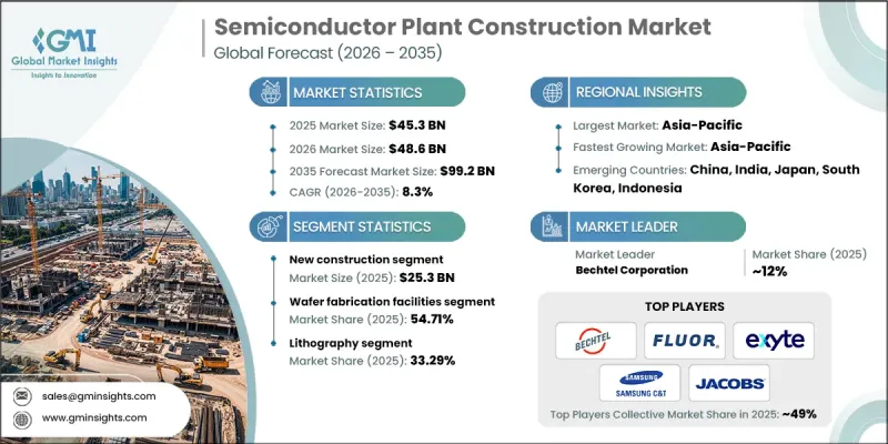
市场成长的驱动力在于先进半导体製造设施和特殊半导体製造设施对半导体製造需求的持续成长。各国政府和私人投资者正大力投资兴建下一代半导体晶圆厂,尤其是在新兴经济体,旨在增强国内产能。这些製造工厂需要高度可控的环境,包括先进的无尘室和精密空调系统,以满足严格的污染标准。特种晶圆厂还需要客製化的基础设施和复杂的公用设施集成,以支援小众半导体製程。新兴地区凭藉着成本优势和旨在扩大高科技製造业的政策奖励,持续吸引资本投资。为了跟上不断加快的进度,承包商越来越多地采用模组化和预製构件的建造方法,以提高效率和品管。扩大半导体产能对于增强全球供应链的韧性以及满足电子、汽车和工业领域日益增长的需求至关重要。资料中心、人工智慧应用和高效能运算基础设施的成长也是推动这一趋势的另一个动力,所有这些都需要不断提高晶片产能。
| 市场范围 | |
|---|---|
| 开始年份 | 2025 |
| 预测年份 | 2026-2035 |
| 起始金额 | 453亿美元 |
| 预测金额 | 992亿美元 |
| 复合年增长率 | 8.3% |
预计到2025年,新建设市场规模将达253亿美元,并在2026年至2035年间以7.5%的复合年增长率成长。随着越来越多的製造商寻求能够容纳先进晶圆製造技术的专用工厂,对新建半导体製造厂的需求仍然强劲。新建工厂能够无缝整合最先进的无尘室系统、最佳化的生产布局以及符合现代製造需求的节能机械系统。全球半导体消费量的成长持续推动待开发区案的投资。此外,新建设还能确保符合严格的污染控制通讯协定、运作安全要求和设备性能标准。
微影术技术目前占据33.29%的市场份额,预计2026年至2035年将以7.8%的复合年增长率成长。微影术设备在将复杂电路图案转移到硅晶圆上方面发挥着至关重要的作用,是先进半导体製造的核心。精密图形化技术对于实现更精细的製程节点和更高的装置性能至关重要。对高效能电子元件和下一代运算解决方案日益增长的需求正在推动对先进微影术设备的投资。极紫外光微影术(EUV)等技术显着提高了装置密度和加工能力,但也导致装置结构日益复杂,对专用设备的安装要求也越来越高。
中国半导体工厂建设市场预计到2025年将达到88亿美元,并在2035年之前以8.8%的复合年增长率持续成长。政府对国内半导体製造业的大力支持以及先进电子基础设施的不断完善,巩固了中国在半导体行业的市场主导地位。随着晶圆代工和晶圆製造产能的扩张,对符合污染控制要求的高精度建设项目的需求日益增长。开发商正着力采用模组化和扩充性的工厂设计,以缩短计划週期,同时确保符合严格的国际标准。消费性电子、汽车半导体研发和先进通讯网路等领域不断增长的生产需求,也持续推动建设活动。
目录
第一章:调查方法和范围
第二章执行摘要
第三章业界考察
- 生态系分析
- 供应商情况
- 利润率
- 每个阶段增加的价值
- 影响价值链的因素
- 影响产业的因素
- 促进因素
- 全球电子和汽车产业对先进半导体的需求不断增长。
- 资料中心、人工智慧和高效能运算基础设施的扩展
- 政府激励措施和补贴以支持国内半导体製造
- 挑战与困难
- 与製造和设备安装相关的资本支出极高。
- 复杂的监管和环境核准流程
- 机会
- 新兴地区先进专业製造设施建设增加。
- 对模组化洁净室和预製製造组件的需求增加。
- 促进因素
- 成长潜力分析
- 未来市场趋势
- 科技与创新趋势
- 当前技术趋势
- 新兴技术
- 价格趋势
- 按地区
- 副产品
- 监理情势
- 标准和合规要求
- 区域法规结构
- 认证标准
- 波特的分析
- PESTEL 分析
第四章 竞争情势
- 介绍
- 企业市占率分析
- 按地区
- 北美洲
- 欧洲
- 亚太地区
- 拉丁美洲
- 中东和非洲
- 按地区
- 公司矩阵分析
- 主要市场公司的竞争分析
- 竞争定位矩阵
- 主要进展
- 併购
- 伙伴关係与合作
- 新产品发布
- 扩张计划
第五章 市场估价与预测:依建筑类型划分,2022-2035年
- 新建设
- 扩张
- 维修
第六章 市场估价与预测:依设施类型划分,2022-2035年
- 晶圆製造厂
- 组装和测试设施
- 研究与开发设施
第七章 市场估计与预测:依设备类型划分,2022-2035年
- 微影术
- 成膜
- 蚀刻
- 化学机械抛光(CMP)
- 打扫
- 其他的
第八章 市场估计与预测:依地区划分,2022-2035年
- 北美洲
- 我们
- 加拿大
- 欧洲
- 德国
- 英国
- 法国
- 义大利
- 西班牙
- 亚太地区
- 中国
- 印度
- 日本
- 韩国
- 澳洲
- 拉丁美洲
- 巴西
- 墨西哥
- 阿根廷
- 中东和非洲
- 沙乌地阿拉伯
- 阿拉伯聯合大公国
- 南非
第九章:公司简介
- Bechtel Corporation
- DPR Construction
- Exyte
- Fluor Corporation
- Gilbane Building Company
- Hensel Phelps
- Intel Construction
- Jacobs Engineering Group
- KBR, Inc
- PCL Construction
- Samsung C&T
- SK ecoplant
- Skanska
- Toyo Engineering Corporation
- Turner Construction Company
The Global Semiconductor Plant Construction Market was valued at USD 45.3 billion in 2025 and is estimated to grow at a CAGR of 8.3% to reach USD 99.2 billion by 2035.
Market growth is driven by rising semiconductor manufacturing demand across both advanced and specialty fabrication facilities. Governments and private investors are allocating significant funding to develop next-generation semiconductor fabs, particularly in emerging economies seeking to strengthen domestic production capabilities. These fabrication plants require highly controlled environments, including advanced cleanrooms and precision HVAC systems designed to meet strict contamination standards. Specialty fabs also demand customized infrastructure and complex utility integration to support niche semiconductor processes. Emerging regions continue to attract capital investment due to cost advantages and policy incentives aimed at expanding high-tech manufacturing. To meet accelerated timelines, contractors increasingly rely on modular and prefabricated construction approaches that enhance efficiency and quality control. Expanding semiconductor capacity is essential for reinforcing global supply chain resilience and addressing rising demand from electronics, automotive, and industrial sectors. Additional momentum is coming from the growth of data centers, artificial intelligence applications, and high-performance computing infrastructure, all of which require increased chip production capacity.
| Market Scope | |
|---|---|
| Start Year | 2025 |
| Forecast Year | 2026-2035 |
| Start Value | $45.3 Billion |
| Forecast Value | $99.2 Billion |
| CAGR | 8.3% |
The new construction segment generated USD 25.3 billion in 2025 and is forecast to grow at a CAGR of 7.5% between 2026 and 2035. Demand for newly built semiconductor facilities remains strong as manufacturers seek purpose-built plants that support advanced wafer fabrication technologies. Constructing new facilities enables seamless integration of state-of-the-art cleanroom systems, optimized production layouts, and energy-efficient mechanical systems tailored to modern manufacturing requirements. Rising global semiconductor consumption continues to encourage investment in greenfield developments. New construction also ensures compliance with rigorous contamination control protocols, operational safety requirements, and equipment performance standards.
The lithography segment held a 33.29% share and is expected to grow at a CAGR of 7.8% from 2026 to 2035. Lithography systems play a critical role in transferring intricate circuit patterns onto silicon wafers, making them central to advanced semiconductor production. Precision patterning technologies are essential for achieving smaller process nodes and higher device performance. Increasing demand for high-efficiency electronic components and next-generation computing solutions is driving investment in advanced lithography equipment. Technologies such as extreme ultraviolet lithography significantly enhance device density and processing capabilities, contributing to higher construction complexity and specialized equipment installation requirements.
China Semiconductor Plant Construction Market reached USD 8.8 billion in 2025 and is anticipated to grow at a CAGR of 8.8% through 2035. Strong government backing for domestic chip manufacturing and the expansion of advanced electronics infrastructure underpins China's market leadership. Growth in foundry and wafer fabrication capacity has intensified demand for highly precise construction that can support contamination-controlled environments. Developers emphasize modular and scalable facility designs to accelerate project delivery while maintaining compliance with stringent international standards. Expanding production requirements linked to consumer electronics, automotive semiconductor development, and advanced communications networks continue to drive additional construction activity.
Major companies operating in the Global Semiconductor Plant Construction Market include Bechtel Corporation, DPR Construction, Exyte, Fluor Corporation, Gilbane Building Company, Hensel Phelps, Intel Construction, Jacobs Engineering Group, KBR, Inc., PCL Construction, Samsung C&T, SK ecoplant, Skanska, Toyo Engineering Corporation, and Turner Construction Company. Companies active in the semiconductor plant construction industry are strengthening their competitive position through strategic partnerships, technological innovation, and geographic expansion. Leading contractors are investing in advanced project management tools, digital modeling technologies, and modular construction capabilities to accelerate timelines and improve precision. Many firms are forming alliances with semiconductor manufacturers to deliver turnkey solutions that integrate design, engineering, and construction expertise. Expanding operations into emerging markets allows companies to capitalize on government incentives and rising fabrication investments.
Table of Contents
Chapter 1 Methodology & Scope
- 1.1 Market scope and definition
- 1.2 Research design
- 1.2.1 Research approach
- 1.2.2 Data collection methods
- 1.3 Data mining sources
- 1.3.1 Global
- 1.3.2 Regional/Country
- 1.4 Base estimates and calculations
- 1.4.1 Base year calculation
- 1.4.2 Key trends for market estimation
- 1.5 Primary research and validation
- 1.5.1 Primary sources
- 1.6 Forecast model
- 1.7 Research assumptions and limitations
Chapter 2 Executive Summary
- 2.1 Industry 360° synopsis
- 2.2 Key market trends
- 2.2.1 Regional
- 2.2.2 Burner design
- 2.2.3 Installation
- 2.2.4 Power Range
- 2.2.5 End Use Industry
- 2.3 CXO perspectives: Strategic imperatives
- 2.3.1 Key decision points for industry executives
- 2.3.2 Critical success factors for market players
- 2.4 Future outlook and strategic recommendations
Chapter 3 Industry Insights
- 3.1 Industry ecosystem analysis
- 3.1.1 Supplier landscape
- 3.1.2 Profit margin
- 3.1.3 Value addition at each stage
- 3.1.4 Factor affecting the value chain
- 3.2 Industry impact forces
- 3.2.1 Growth drivers
- 3.2.1.1 Rising global demand for advanced semiconductors across electronics and automotive sectors
- 3.2.1.2 Expansion of data centers, AI, and high-performance computing infrastructure
- 3.2.1.3 Government incentives and subsidies supporting domestic semiconductor manufacturing
- 3.2.2 Pitfalls & Challenges
- 3.2.2.1 Extremely high capital expenditure for fab construction and tooling
- 3.2.2.2 Complex regulatory and environmental approval processes
- 3.2.3 Opportunities
- 3.2.3.1 Rising construction of advanced and specialty fabs in emerging regions
- 3.2.3.2 Growing demand for modular cleanroom and prefabricated fab components
- 3.2.1 Growth drivers
- 3.3 Growth potential analysis
- 3.4 Future market trends
- 3.5 Technology and innovation landscape
- 3.5.1 Current technological trends
- 3.5.2 Emerging technologies
- 3.6 Price trends
- 3.6.1 By region
- 3.6.2 By product
- 3.7 Regulatory landscape
- 3.7.1 Standards and compliance requirements
- 3.7.2 Regional regulatory frameworks
- 3.7.3 Certification standards
- 3.8 Porter’s analysis
- 3.9 PESTEL analysis
Chapter 4 Competitive Landscape, 2025
- 4.1 Introduction
- 4.2 Company market share analysis
- 4.2.1 By Region
- 4.2.1.1 North America
- 4.2.1.2 Europe
- 4.2.1.3 Asia Pacific
- 4.2.1.4 Latin America
- 4.2.1.5 Middle East & Africa
- 4.2.1 By Region
- 4.3 Company matrix analysis
- 4.4 Competitive analysis of major market players
- 4.5 Competitive positioning matrix
- 4.6 Key developments
- 4.6.1 Mergers & acquisitions
- 4.6.2 Partnerships & collaborations
- 4.6.3 New product launches
- 4.6.4 Expansion plans
Chapter 5 Market Estimates & Forecast, By Construction Type, 2022 - 2035, (USD Billion) (Thousand Units)
- 5.1 Key trends
- 5.2 New construction
- 5.3 Expansion
- 5.4 Renovation
Chapter 6 Market Estimates & Forecast, By Facility, 2022 - 2035, (USD Billion) (Thousand Units)
- 6.1 Key trends
- 6.2 Wafer fabrication facilities
- 6.3 Assembly & test facilities
- 6.4 Research & development facilities
Chapter 7 Market Estimates & Forecast, By Equipment, 2022 - 2035, (USD Billion) (Thousand Units)
- 7.1 Key trends
- 7.2 Lithography
- 7.3 Deposition
- 7.4 Etching
- 7.5 Chemical mechanical planarization (CMP)
- 7.6 Cleaning
- 7.7 Others
Chapter 8 Market Estimates & Forecast, By Region, 2022 - 2035, (USD Billion) (Thousand Units)
- 8.1 Key trends
- 8.2 North America
- 8.2.1 U.S.
- 8.2.2 Canada
- 8.3 Europe
- 8.3.1 Germany
- 8.3.2 UK
- 8.3.3 France
- 8.3.4 Italy
- 8.3.5 Spain
- 8.4 Asia Pacific
- 8.4.1 China
- 8.4.2 India
- 8.4.3 Japan
- 8.4.4 South Korea
- 8.4.5 Australia
- 8.5 Latin America
- 8.5.1 Brazil
- 8.5.2 Mexico
- 8.5.3 Argentina
- 8.6 MEA
- 8.6.1 Saudi Arabia
- 8.6.2 UAE
- 8.6.3 South Africa
Chapter 9 Company Profiles
- 9.1 Bechtel Corporation
- 9.2 DPR Construction
- 9.3 Exyte
- 9.4 Fluor Corporation
- 9.5 Gilbane Building Company
- 9.6 Hensel Phelps
- 9.7 Intel Construction
- 9.8 Jacobs Engineering Group
- 9.9 KBR, Inc
- 9.10 PCL Construction
- 9.11 Samsung C&T
- 9.12 SK ecoplant
- 9.13 Skanska
- 9.14 Toyo Engineering Corporation
- 9.15 Turner Construction Company
 2025年半导体工厂建设全球市场报告
 全球半导体工厂计划- 特别报告:Project Insight
 半导体工厂建设市场,按建设、按设施、按设备、按基础设施、按国家和地区 - 2024-2032 年行业分析、市场规模、市场份额和预测