


 |
市场调查报告书
商品编码
1982377
薄晶圆市场机会、成长要素、产业趋势分析及2026-2035年预测。Thin Wafer Market Opportunity, Growth Drivers, Industry Trend Analysis, and Forecast 2026 - 2035 |
||||||
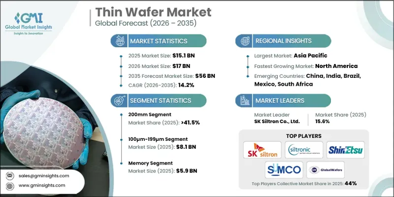
全球薄晶圆市场预计到 2025 年价值 151 亿美元,预计到 2035 年将达到 560 亿美元,年复合成长率为 14.2%。
超薄晶圆是采用先进的背面研磨、精密抛光和化学蚀刻技术加工而成的半导体基板,其厚度可达200微米或更薄(表面处理后通常为50微米至100微米)。这些超薄基板对于新一代功率元件和紧凑型电子架构至关重要,尤其是在需要高密度整合且总厚度偏差控制在1微米以内的3D堆迭应用中。其结构均匀性最大限度地减少了翘曲,并确保了在先进封装製程中的可靠操作。对小型电子设备、高效能运算和高效能电源管理解决方案日益增长的需求正在加速超薄晶圆在各行各业的应用。半导体製造技术和材料工程的不断进步进一步提高了晶圆的耐久性、产量比率和电气性能,使超薄晶圆成为现代半导体製造的基本组成部分。
| 市场范围 | |
|---|---|
| 开始年份 | 2025 |
| 预测期 | 2026-2035 |
| 上市时的市场规模 | 151亿美元 |
| 预计金额 | 560亿美元 |
| 复合年增长率 | 14.2% |
汽车产业电气化和自动化技术的进步显着推动了对薄晶圆的需求成长。不断提高的车辆燃油效率标准和减少排放气体的努力正在加速先进半导体元件的整合。新兴市场电动车的日益普及,以及对充电基础设施和电子控制技术的投资,正在推动市场扩张。此外,公共和私人对半导体生产投资的增加,以及主要企业之间活性化的研发合作,正在加速技术进步并扩大製造能力。
预计2026年至2035年间,125mm/150mm晶圆尺寸市场将以13.8%的复合年增长率成长。推动这一市场成长的主要因素是汽车产业对紧凑型、高效能功率积体电路和感测器解决方案的需求不断增长。连网型设备、先进通讯基础设施和家用电子电器的普及,持续推动成熟节点製造流程的发展,这些製程利用较小的晶圆尺寸来实现更具成本效益的生产。
预计到2025年,厚度为100μm至199μm的薄晶圆市场规模将达到81亿美元。由于其在功率半导体应用中的日益普及,尤其是在支援电动车和可再生能源系统方面,该细分市场占据了最大的市场份额。此厚度范围内的薄晶圆在机械强度和电气效率之间实现了最佳平衡,从而支援感测器、电源管理积体电路和先进3D封装架构的大规模生产。製造商正致力于开发先进的瞬态键合解决方案和载流子晶圆技术,以提高高功率半导体装置的製程稳定性和性能。
预计到2025年,北美薄晶圆市场将占据15.7%的市场。这一区域成长主要得益于汽车平台向电气化转型,而电气化汽车平台则需要更高的半导体负载能力来支援先进的控制和安全系统。医疗设备製造业的扩张、人口结构变化以及对半导体製造的策略性投资,都将推动该地区在2035年之前持续发展。
目录
第一章:调查方法和范围
第二章执行摘要
第三章业界考察
- 生态系分析
- 供应商情况
- 利润率
- 成本结构
- 每个阶段增加的价值
- 影响价值链的因素
- 中断
- 影响产业的因素
- 促进因素
- 对先进半导体封装的需求
- 5G和人工智慧晶片的普及
- 物联网设备的广泛应用
- 电动车的电力电子设备
- CMOS影像感测器的发展
- 产业潜在风险与挑战
- 晶圆翘曲和处理方面的挑战
- 缺陷密度高,良率产量比率
- 市场机会
- 先进包装创新
- 功率半导体领域的转变
- 促进因素
- 成长潜力分析
- 监理情势
- 北美洲
- 欧洲
- 亚太地区
- 拉丁美洲
- 中东和非洲
- 波特的分析
- PESTEL 分析
- 科技与创新趋势
- 当前技术趋势
- 新兴技术
- 价格趋势
- 历史价格分析(2022-2024)
- 影响价格趋势的因素
- 各地区价格波动
- 价格预测(2026-2035)
- 定价策略
- 新兴经营模式
- 合规要求
- 专利分析
第四章 竞争情势
- 介绍
- 企业市占率分析
- 按地区
- 北美洲
- 欧洲
- 亚太地区
- 拉丁美洲
- 中东和非洲
- 市场集中度分析
- 按地区
- 主要企业的竞争标竿分析
- 财务绩效比较
- 销售量
- 利润率
- 研究与开发
- 产品系列比较
- 产品线
- 科技
- 创新
- 区域扩张比较
- 全球扩张分析
- 服务网路覆盖
- 按地区分類的市场渗透率
- 竞争定位矩阵
- 领导者
- 挑战者
- 追踪者
- 小众玩家
- 战略展望矩阵
- 财务绩效比较
- 2022-2025 年重大发展
- 併购
- 伙伴关係和联盟
- 技术进步
- 业务拓展与投资策略
- 永续发展倡议
- 数位转型计划
- 新兴/Start-Ups竞争对手的发展趋势
第五章 市场估计与预测:依厚度划分,2022-2035年
- ,
- 超过 200μm
- 100微米至199微米
- 50微米至99微米
- 30微米至49微米
- 10微米至29微米
- 小于10微米
第六章 依晶圆尺寸分類的市场估算与预测,2022-2035年
- 100 mm
- 125 mm/150 mm
- 200 mm
- 300 mm
第七章 市场估价与预测:依製程划分,2022-2035年
- 暂时黏合剥离
- UV释放黏合剂
- 黏合剂
- 溶剂释放黏合剂
- 无载体系统/泰科工艺
第八章 市场估计与预测:依应用领域划分,2022-2035年
- MEMS
- CMOS影像感测器
- 记忆
- 射频设备
- LED
- 中介
- 逻辑
- 其他的
第九章 市场估计与预测:依地区划分,2022-2035年
- 按地区
- 北美洲
- 我们
- 加拿大
- 欧洲
- 英国
- 德国
- 法国
- 义大利
- 西班牙
- 荷兰
- 其他欧洲地区
- 亚太地区
- 中国
- 印度
- 日本
- 韩国
- 澳洲
- 亚太其他地区
- 拉丁美洲
- 巴西
- 墨西哥
- 阿根廷
- 其他拉丁美洲地区
- 中东和非洲(MEA)
- 沙乌地阿拉伯
- 南非
- 阿拉伯聯合大公国
- 其他中东和非洲地区
第十章:公司简介
- 3M
- Applied Materials
- Brewer Science
- Disco Corporation
- EV Group
- GlobalWafers Co. Ltd.
- IceMOS Technology Ltd.
- Mechatronic Systemtechnik GmbH
- Okmetic
- Polishing Corporation of America
- Shanghai Simgui Technology Co. Ltd.
- Shin-Etsu Chemical Co., Ltd.
- Silicon Valley Microelectronics, Inc
- Siltronic AG
- Sil'tronix Silicon Technologies
- SK Siltron Co., Ltd.
- Skynova SA
- SOITEC
- SUMCO CORPORATION
- SUSS MicroTec
- UniversityWafer, Inc
- Virginia Semiconductor Inc.
- Wafer Works Corporation
- Wafer World Inc.
- WaferPro
The Global Thin Wafer Market was valued at USD 15.1 billion in 2025 and is estimated to grow at a CAGR of 14.2% to reach USD 56 billion by 2035.
Thin wafers are semiconductor substrates processed through advanced back grinding, precision polishing, and chemical etching techniques to achieve a thickness of 200μm or below, typically ranging between 50μm and 100μm after front-side fabrication. These ultra-thin substrates are critical for next-generation power devices and compact electronic architectures, particularly in 3D stacking applications where high-density integration is required without exceeding 1μm total thickness variation. Their structural uniformity minimizes warping while enabling reliable handling during advanced packaging processes. Rising demand for miniaturized electronics, high-performance computing, and efficient power management solutions is accelerating adoption across multiple industries. Continuous advancements in semiconductor fabrication technologies and material engineering are further enhancing wafer durability, yield rates, and electrical performance, positioning thin wafers as a foundational component in modern semiconductor manufacturing.
| Market Scope | |
|---|---|
| Start Year | 2025 |
| Forecast Year | 2026-2035 |
| Start Value | $15.1 Billion |
| Forecast Value | $56 Billion |
| CAGR | 14.2% |
Growing electrification and automation within the automotive sector are significantly contributing to thin wafer demand. Increasing vehicle efficiency standards and emission reduction initiatives are driving the integration of advanced semiconductor components. Expanding electric vehicle adoption across emerging economies, along with investments in charging infrastructure and electronic control technologies, is reinforcing market expansion. In addition, public and private sector investments in semiconductor production, combined with rising research and development collaboration among leading players, are accelerating technological progress and manufacturing capacity growth.
The 125 mm/150 mm wafer size segment is expected to grow at a CAGR of 13.8% during 2026-2035. Rising automotive demand for compact and high-efficiency power integrated circuits and sensor solutions is fueling this segment. Broader deployment of connected devices, advanced communication infrastructure, and consumer electronics continues to support mature-node production processes utilizing smaller wafer formats for cost-effective manufacturing.
The 100μm-199μm thickness segment generated USD 8.1 billion in 2025. This segment maintains the largest share due to increasing utilization in power semiconductor applications supporting electric mobility and renewable energy systems. Thin wafers within this thickness range provide an optimal balance between mechanical integrity and electrical efficiency, supporting high-volume sensor manufacturing, power management integrated circuits, and advanced 3D packaging architectures. Manufacturers are emphasizing sophisticated temporary bonding solutions and carrier wafer technologies to improve process stability and performance outcomes in high-power semiconductor devices.
North America Thin Wafer Market accounted for 15.7% share in 2025. Regional growth is supported by the transition toward electrified automotive platforms, which require increased semiconductor content for advanced control and safety systems. Expansion in medical device manufacturing, demographic trends, and strategic semiconductor fabrication investments are contributing to sustained regional development through 2035.
Prominent companies operating in the Global Thin Wafer Market include SUMCO CORPORATION, Shin-Etsu Chemical Co., Ltd., Siltronic AG, GlobalWafers Co. Ltd., SK Siltron Co., Ltd., SOITEC, Applied Materials, Disco Corporation, EV Group, SUSS MicroTec, Okmetic, 3M, Brewer Science, Silicon Valley Microelectronics, Inc., UniversityWafer, Inc., Virginia Semiconductor Inc., Wafer Works Corporation, Shanghai Simgui Technology Co. Ltd., IceMOS Technology Ltd., Mechatronic Systemtechnik GmbH, Polishing Corporation of America, Sil'tronix Silicon Technologies, Skynova SA, Wafer World Inc., and WaferPro. Companies in the Global Thin Wafer Market are strengthening their competitive position through technological innovation, strategic alliances, and capacity expansion. Manufacturers are investing heavily in advanced material processing techniques, precision thinning equipment, and bonding technologies to enhance wafer uniformity and yield performance. Strategic collaborations with semiconductor foundries and device manufacturers enable early integration into next-generation chip designs. Firms are also expanding fabrication facilities to address rising global demand and improve supply chain resilience. Portfolio diversification into specialty substrates and engineered wafer solutions supports broader customer engagement.
Table of Contents
Chapter 1 Methodology and Scope
- 1.1 Market scope and definition
- 1.2 Research design
- 1.2.1 Research approach
- 1.2.2 Data collection methods
- 1.3 Data mining sources
- 1.3.1 Global
- 1.3.2 Regional/Country
- 1.4 Base estimates and calculations
- 1.4.1 Base year calculation
- 1.4.2 Key trends for market estimation
- 1.5 Primary research and validation
- 1.5.1 Primary sources
- 1.6 Forecast model
- 1.7 Research assumptions and limitations
Chapter 2 Executive Summary
- 2.1 Industry snapshot
- 2.2 Key market trends
- 2.2.1 Thickness trends
- 2.2.2 Wafer size trends
- 2.2.3 Process trends
- 2.2.4 Application trends
- 2.2.5 Regional trends
- 2.3 TAM Analysis, 2025-2034 (USD Billion)
- 2.4 CXO perspectives: Strategic imperatives
- 2.4.1 Executive decision points
- 2.4.2 critical success factors
- 2.5 Future outlook and strategic recommendations
Chapter 3 Industry Insights
- 3.1 Industry ecosystem analysis
- 3.1.1 Supplier Landscape
- 3.1.2 Profit Margin
- 3.1.3 Cost structure
- 3.1.4 Value addition at each stage
- 3.1.5 Factor affecting the value chain
- 3.1.6 Disruptions
- 3.2 Industry impact forces
- 3.2.1 Growth drivers
- 3.2.1.1 Advanced Semiconductor Packaging Demand
- 3.2.1.2 5G and AI Chip Proliferation
- 3.2.1.3 IoT Device Expansion
- 3.2.1.4 Electric Vehicle Power Electronics
- 3.2.1.5 CMOS Image Sensor Growth
- 3.2.2 Industry pitfalls and challenges
- 3.2.2.1 Wafer Warpage and Handling Challenges
- 3.2.2.2 High Defect Density and Yield Loss
- 3.2.3 Market opportunities
- 3.2.3.1 Advanced Packaging Innovation
- 3.2.3.2 Power Semiconductor Shift
- 3.2.1 Growth drivers
- 3.3 Growth potential analysis
- 3.4 Regulatory landscape
- 3.4.1 North America
- 3.4.2 Europe
- 3.4.3 Asia Pacific
- 3.4.4 Latin America
- 3.4.5 Middle East & Africa
- 3.5 Porter’s analysis
- 3.6 PESTEL analysis
- 3.7 Technology and innovation landscape
- 3.7.1 Current technological trends
- 3.7.2 Emerging technologies
- 3.8 Price trends
- 3.8.1 Historical price analysis (2022-2024)
- 3.8.2 Price trend drivers
- 3.8.3 Regional price variations
- 3.8.4 Price forecast (2026-2035)
- 3.9 Pricing strategies
- 3.10 Emerging business models
- 3.11 Compliance requirements
- 3.12 Patent analysis
Chapter 4 Competitive Landscape, 2025
- 4.1 Introduction
- 4.2 Company market share analysis
- 4.2.1 By Region
- 4.2.1.1 North America
- 4.2.1.2 Europe
- 4.2.1.3 Asia Pacific
- 4.2.1.4 Latin America
- 4.2.1.5 Middle East & Africa
- 4.2.2 Market Concentration Analysis
- 4.2.1 By Region
- 4.3 Competitive benchmarking of key players
- 4.3.1 Financial performance comparison
- 4.3.1.1 Revenue
- 4.3.1.2 Profit margin
- 4.3.1.3 R&D
- 4.3.2 Product portfolio comparison
- 4.3.2.1 Product range breadth
- 4.3.2.2 Technology
- 4.3.2.3 Innovation
- 4.3.3 Geographic presence comparison
- 4.3.3.1 Global footprint analysis
- 4.3.3.2 Service network coverage
- 4.3.3.3 Market penetration by region
- 4.3.4 Competitive positioning matrix
- 4.3.4.1 Leaders
- 4.3.4.2 Challengers
- 4.3.4.3 Followers
- 4.3.4.4 Niche players
- 4.3.5 Strategic outlook matrix
- 4.3.1 Financial performance comparison
- 4.4 Key developments, 2022-2025
- 4.4.1 Mergers and acquisitions
- 4.4.2 Partnerships and collaborations
- 4.4.3 Technological advancements
- 4.4.4 Expansion and investment strategies
- 4.4.5 Sustainability initiatives
- 4.4.6 Digital transformation initiatives
- 4.5 Emerging/ startup competitors landscape
Chapter 5 Market Estimates & Forecast, By Thickness, 2022 - 2035 (USD Million)
- 5.1 Key trends,
- 5.2 >200μm
- 5.3 100μm-199μm
- 5.4 50μm-99μm
- 5.5 30μm-49μm
- 5.6 10μm-29μm
- 5.7 <10μm
Chapter 6 Market Estimates and Forecast, By Wafer Size, 2022 - 2035 (USD Million)
- 6.1 Key trends
- 6.2 100 mm
- 6.3 125 mm/150mm
- 6.4 200 mm
- 6.5 300 mm
Chapter 7 Market Estimates and Forecast, By Process, 2022 - 2035 (USD Million)
- 7.1 Key trends
- 7.2 Temporary bonding & debonding
- 7.2.1 UV-release adhesives
- 7.2.2 Thermal-release adhesives
- 7.2.3 Solvent-release adhesives
- 7.3 Carrier-less approach/Taiko process
Chapter 8 Market Estimates and Forecast, By Application, 2022 - 2035 (USD Million)
- 8.1 Key trends
- 8.2 MEMS
- 8.3 CMOS image sensors
- 8.4 Memory
- 8.5 RF devices
- 8.6 LED
- 8.7 Interposers
- 8.8 Logic
- 8.9 Others
Chapter 9 Market Estimates & Forecast, By Region, 2022 - 2035 (USD Million)
- 9.1 Key trends, by region
- 9.2 North America
- 9.2.1 U.S.
- 9.2.2 Canada
- 9.3 Europe
- 9.3.1 UK
- 9.3.2 Germany
- 9.3.3 France
- 9.3.4 Italy
- 9.3.5 Spain
- 9.3.6 Netherlands
- 9.3.7 Rest of Europe
- 9.4 Asia-Pacific
- 9.4.1 China
- 9.4.2 India
- 9.4.3 Japan
- 9.4.4 South Korea
- 9.4.5 Australia
- 9.4.6 Rest of Asia-Pacific
- 9.5 Latin America
- 9.5.1 Brazil
- 9.5.2 Mexico
- 9.5.3 Argentina
- 9.5.4 Rest of Latin America
- 9.6 MEA
- 9.6.1 Saudi Arabia
- 9.6.2 South Africa
- 9.6.3 UAE
- 9.6.4 Rest of MEA
Chapter 10 Company Profiles
- 10.1 3M
- 10.2 Applied Materials
- 10.3 Brewer Science
- 10.4 Disco Corporation
- 10.5 EV Group
- 10.6 GlobalWafers Co. Ltd.
- 10.7 IceMOS Technology Ltd.
- 10.8 Mechatronic Systemtechnik GmbH
- 10.9 Okmetic
- 10.10 Polishing Corporation of America
- 10.11 Shanghai Simgui Technology Co. Ltd.
- 10.12 Shin-Etsu Chemical Co., Ltd.
- 10.13 Silicon Valley Microelectronics, Inc
- 10.14 Siltronic AG
- 10.15 Sil'tronix Silicon Technologies
- 10.16 SK Siltron Co., Ltd.
- 10.17 Skynova SA
- 10.18 SOITEC
- 10.19 SUMCO CORPORATION
- 10.20 SUSS MicroTec
- 10.21 UniversityWafer, Inc
- 10.22 Virginia Semiconductor Inc.
- 10.23 Wafer Works Corporation
- 10.24 Wafer World Inc.
- 10.25 WaferPro
 薄晶圆市场:依材料、晶圆尺寸、製造流程、应用和最终用途产业划分-2026-2032年全球市场预测
 全球薄晶圆市场规模、份额、趋势和成长分析报告(2026-2034)薄晶圆FOSB市场:依晶圆直径、材料类型、厚度范围、表面处理、应用、终端用户产业和分销管道划分-全球预测,2026-2032年薄晶圆FOUP市场:2026年至2032年全球预测(依晶圆尺寸、产品类型、产能、材质、自动化程度、最终用户和应用划分)
 全球薄晶圆市场:依厚度、应用、材料、终端用户产业、国家及地区划分-产业分析、市场规模、份额及未来预测(2025-2032年)
 2026年全球薄晶圆市场报告
 2026-2030年全球磷化铟(InP)晶圆市场薄晶圆市场-2025年至2030年的预测