


 |
市场调查报告书
商品编码
1982387
SiC晶圆回收服务市场:商业机会、成长要素、产业趋势分析及2026-2035年预测。SiC Wafer Reclaim Services Market Opportunity, Growth Drivers, Industry Trend Analysis, and Forecast 2026 - 2035 |
||||||
全球碳化硅晶圆回收服务市场预计到 2025 年将达到 6.84 亿美元,年复合成长率为 8.4%,到 2035 年将达到 15 亿美元。
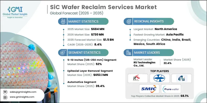
这一成长主要得益于电动车 (EV) 的快速普及,从而提升了对碳化硅 (SiC) 基功率装置的需求,这些装置广泛应用于牵引逆变器、车载充电器和电源管理系统等领域。这些装置因其高效率、优异的产量比率性和耐压性而备受青睐。政府支持半导体製造的各项倡议,包括奖励、补贴和晶圆厂扩建计划,进一步推动了晶圆回收服务的需求。晶圆回收已成为一项至关重要且经济高效的製造策略,能够提高良率并减少材料废弃物。晶圆直径不断增大,尤其是 150 毫米和 200 毫米晶圆,这需要先进的抛光、侦测和表面特性分析工具。服务供应商正在整合先进的测量和污染控制技术,以提供高品质的回收晶圆,满足汽车和工业电力电子领域日益严格的平整度和缺陷接受度要求。
| 市场范围 | |
|---|---|
| 开始年份 | 2025 |
| 预测期 | 2026-2035 |
| 上市时的市场规模 | 6.84亿美元 |
| 预测金额 | 15亿美元 |
| 复合年增长率 | 8.4% |
上文提到的10吋(超过250毫米)晶圆市场预计将在2026年至2035年间以8.9%的复合年增长率成长。超大尺寸晶圆对于下一代功率元件至关重要,但其加工需要专用设备、精确的层去除和先进的抛光技术,以防止开裂、翘曲或污染。製造商正在改进这些工艺,以最大限度地减少材料损失、降低生产成本,并支援碳化硅元件在汽车、工业和能源领域的大规模应用。
预计到2025年,研磨和抛光服务市场规模将达到1.681亿美元,并在2026年至2035年间以8.8%的复合年增长率成长。这些服务专注于实现碳化硅晶圆的高精度平整度、厚度和表面光滑度。自动化、製程监控和先进抛光材料的使用正日益广泛地应用于提高产量比率、最大限度地减少晶圆间差异并增强製程一致性。客製化的研磨和抛光解决方案正被应用于满足高功率电动车模组、工业转换器和其他特殊应用的需求,使晶圆厂能够在降低成本的同时交付可靠的晶圆。
预计2025年,北美碳化硅晶圆回收服务市占率将达33.6%。该地区受益于成熟的半导体生态系统、碳化硅元件在汽车和工业领域的高渗透率以及先进的研究基础设施。此外,美国和加拿大对清洁能源的重视也进一步推动了市场成长。
目录
第一章:调查方法和范围
第二章执行摘要
第三章业界考察
- 生态系分析
- 供应商情况
- 利润率分析
- 成本结构
- 每个阶段增加的价值
- 影响价值链的因素
- 中断
- 影响产业的因素
- 促进因素
- 家用电子电器。
- 半导体在太阳能发电领域的应用日益广泛
- SiC晶圆在5G和物联网设备中的广泛应用
- 电动车(EV)的广泛普及
- 政府主导的扩大半导体製造规模的倡议日益增多
- 产业潜在风险与挑战
- 製造工厂维修成本高昂
- 高产产量比率回收製程的技术挑战
- 市场机会
- 进入新兴电动车製造地和新工厂
- 开发针对先进功率设备的优质回收服务
- 促进因素
- 监理情势
- 北美洲
- 欧洲
- 亚太地区
- 拉丁美洲
- 中东和非洲
- 波特的分析
- PESTEL 分析
- 科技与创新趋势
- 当前技术趋势
- 新兴技术
- 新兴经营模式
- 合规要求
- 专利和智慧财产权分析
- 地缘政治和贸易趋势
第四章 竞争情势
- 介绍
- 企业市占率分析
- 按地区
- 北美洲
- 欧洲
- 亚太地区
- 拉丁美洲
- 中东和非洲
- 按地区
- 主要企业的竞争标竿分析
- 财务绩效比较
- 销售量
- 利润率
- 研究与开发
- 产品系列比较
- 产品线宽度
- 科技
- 创新
- 区域部署对比
- 全球扩张分析
- 服务网路覆盖
- 按地区分類的市场渗透率
- 竞争定位矩阵
- 领导者
- 挑战者
- 追踪者
- 小众玩家
- 财务绩效比较
- 2022-2025 年重大发展
- 併购
- 伙伴关係和联盟
- 技术进步
- 业务拓展与投资策略
- 数位转型计划
- 新兴/Start-Ups竞争对手的发展趋势
第五章 市场估算与预测:服务类型,2022-2035年
- 外延层去除
- 研磨和抛光服务
- 化学机械抛光(CMP)
- 表面抛光服务
- 清洁和检查服务
- 其他的
第六章 市场估算与预测:依晶圆直径划分,2022-2035年
- 小于 5 英吋(100-125 毫米)
- 5-10吋(125-250毫米)
- 超过 10 吋(超过 250 毫米)
第七章 市场估计与预测:依復苏阶段划分,2022-2035年
- 外延后回收
- 设备製造后的翻新
- 测试和品管后的再生
- 未使用晶圆的回收利用
第八章 市场估算与预测:依最终用途划分,2022-2035年
- 车
- 工业和製造业
- 通讯和数据中心
- 家用电子电器
- 可再生能源
- 航太/国防
- 其他的
第九章 市场估价与预测:依最终用户划分,2022-2035年
- 半导体製造商(IDM)
- 铸造厂和契约製造
- 研究与发展机构与大学
- 晶圆经销商和仲介业者
第十章 市场估价与预测:依地区划分,2022-2035年
- 北美洲
- 我们
- 加拿大
- 欧洲
- 德国
- 英国
- 法国
- 西班牙
- 义大利
- 荷兰
- 亚太地区
- 中国
- 印度
- 日本
- 澳洲
- 韩国
- 拉丁美洲
- 巴西
- 墨西哥
- 阿根廷
- 中东和非洲
- 南非
- 沙乌地阿拉伯
- 阿拉伯聯合大公国
第十一章:公司简介
- 主要企业
- RS Technologies Co., Ltd.
- Phoenix Silicon International Corporation
- Semiconductor Industry Co., Ltd.
- Pure Wafer
- 按地区分類的主要企业
- Mimasu
- TOPCO Scientific
- Scientech Corporation
- 特殊玩家/干扰者
- Kinik Company
- NOVA Electronic Materials, LLC
- Silicon Materials Inc.
- GlobalWafers Co., Ltd.
- II-VI Incorporated
- STMicroelectronics
- ROHM Co., Ltd.
- Wolfspeed, A Cree Company
- Norstel AB
- GT Advanced Technologies
- DOWA Electronics Materials Co., Ltd.
- Siltronic AG
- Wafer World Inc.
The Global SiC Wafer Reclaim Services Market was valued at USD 684 million in 2025 and is estimated to grow at a CAGR of 8.4% to reach USD 1.5 billion by 2035.
The growth is fueled by the rapid adoption of electric vehicles (EVs), which is increasing demand for silicon carbide-based power devices in applications like traction inverters, onboard chargers, and power management systems. These devices are preferred for their high efficiency, excellent thermal tolerance, and voltage handling capabilities. Government initiatives supporting semiconductor manufacturing, including incentives, subsidies, and fab expansion programs, are further driving demand for wafer reclaim services. Reclaiming wafers has become an essential cost-efficient manufacturing strategy, enabling higher yields and reduced material waste. There is a growing trend toward larger diameter wafers, particularly 150 mm and 200 mm, which requires advanced polishing, inspection, and surface characterization tools. Service providers are integrating sophisticated metrology and contamination control techniques to ensure high-quality reclaimed wafers that meet increasingly stringent flatness and defect tolerance requirements for automotive and industrial power electronics.
| Market Scope | |
|---|---|
| Start Year | 2025 |
| Forecast Year | 2026-2035 |
| Start Value | $684 Million |
| Forecast Value | $1.5 Billion |
| CAGR | 8.4% |
The above 10-inch (>250 mm) wafer segment is expected to grow at a CAGR of 8.9% during 2026-2035. Ultra-large wafers are critical for next-generation power devices, but processing them requires specialized equipment, precise layer removal, and advanced polishing techniques to avoid cracking, warping, or contamination. Manufacturers are refining these processes to minimize material loss, reduce production costs, and support large-scale deployment of SiC devices in automotive, industrial, and energy sectors.
The grinding & lapping services segment generated USD 168.1 million in 2025 and is anticipated to grow at a CAGR of 8.8% during 2026-2035. These services focus on achieving precise flatness, thickness, and surface smoothness for SiC wafers. Automation, process monitoring, and advanced abrasives are increasingly used to improve yields, minimize wafer-to-wafer variability, and enhance process consistency. Customized grinding and lapping solutions are being adopted to meet the requirements of high-power EV modules, industrial converters, and other specialized applications, enabling fabs to deliver reliable wafers while controlling costs.
North America SiC Wafer Reclaim Services Market held a 33.6% share in 2025. The region benefits from a well-established semiconductor ecosystem, strong automotive and industrial adoption of SiC devices, and advanced research infrastructure. A focus on clean energy initiatives further supports market growth across the U.S. and Canada.
Key players in the Global SiC Wafer Reclaim Services Market include Pure Wafer, Kinik Company, TOPCO Scientific, RS Technologies Co., Ltd., NOVA Electronic Materials, LLC, Scientech Corporation, Phoenix Silicon International Corporation, Semiconductor Industry Co., Ltd., and Mimasu. Companies in the Global SiC Wafer Reclaim Services Market are strengthening their positions by expanding their service capabilities, investing in advanced polishing and metrology technologies, and offering customized reclaim solutions for different wafer diameters and applications. Strategies include integrating automation and process monitoring to improve yields and reduce costs, developing proprietary methods for high-yield, low-defect wafer processing, and forming partnerships with semiconductor fabs to ensure a steady service pipeline. Firms are also exploring ultra-large wafer reclaim processes to meet the growing demand from automotive, industrial, and energy sectors, enhancing scalability and operational efficiency while maintaining high-quality standards.
Table of Contents
Chapter 1 Methodology and Scope
- 1.1 Market scope and definition
- 1.2 Research design
- 1.2.1 Research approach
- 1.2.2 Data collection methods
- 1.3 Data mining sources
- 1.3.1 Global
- 1.3.2 Regional/Country
- 1.4 Base estimates and calculations
- 1.4.1 Base year calculation
- 1.4.2 Key trends for market estimation
- 1.5 Primary research and validation
- 1.5.1 Primary sources
- 1.6 Forecast model
- 1.7 Research assumptions and limitations
Chapter 2 Executive Summary
- 2.1 Industry 360° synopsis, 2022 - 2035
- 2.2 Key market trends
- 2.2.1 Service type trends
- 2.2.2 Wafer diameter trends
- 2.2.3 Reclaim stage trends
- 2.2.4 End-use application trends
- 2.2.5 End-user trends
- 2.2.6 Regional trends
- 2.3 TAM analysis, 2025-2034
- 2.4 CXO perspectives: Strategic imperatives
- 2.4.1 Executive decision points
- 2.4.2 Critical success factors
Chapter 3 Industry Insights
- 3.1 Industry ecosystem analysis
- 3.1.1 Supplier landscape
- 3.1.2 Profit margin analysis
- 3.1.3 Cost structure
- 3.1.4 Value addition at each stage
- 3.1.5 Factor affecting the value chain
- 3.1.6 Disruptions
- 3.2 Industry impact forces
- 3.2.1 Growth drivers
- 3.2.1.1 Rising demand of SiC wafers in consumer electronics
- 3.2.1.2 Increasing adoption of semiconductors in solar energy
- 3.2.1.3 Growing penetration of SiC wafers for 5G and IoT devices
- 3.2.1.4 The increasing adoption of electric vehicles (EV)
- 3.2.1.5 Rising government initiative to increase semiconductor manufacturing
- 3.2.2 Industry pitfalls and challenges
- 3.2.2.1 High maintenance cost of manufacturing facilities
- 3.2.2.2 Technical challenges in high-yield reclaim processes
- 3.2.3 Market opportunities
- 3.2.3.1 Penetration into emerging EV manufacturing hubs and new fabs
- 3.2.3.2 Development of premium reclaim services for advanced power devices
- 3.2.1 Growth drivers
- 3.3 Regulatory landscape
- 3.3.1 North America
- 3.3.2 Europe
- 3.3.3 Asia Pacific
- 3.3.4 Latin America
- 3.3.5 Middle East & Africa
- 3.4 Porter’s analysis
- 3.5 PESTEL analysis
- 3.6 Technology and innovation landscape
- 3.6.1 Current technological trends
- 3.6.2 Emerging technologies
- 3.7 Emerging business models
- 3.8 Compliance requirements
- 3.9 Patent and IP analysis
- 3.10 Geopolitical and trade dynamics
Chapter 4 Competitive Landscape, 2025
- 4.1 Introduction
- 4.2 Company market share analysis
- 4.2.1 By region
- 4.2.1.1 North America
- 4.2.1.2 Europe
- 4.2.1.3 Asia Pacific
- 4.2.1.4 Latin America
- 4.2.1.5 Middle East & Africa
- 4.2.1 By region
- 4.3 Competitive benchmarking of key players
- 4.3.1 Financial performance comparison
- 4.3.1.1 Revenue
- 4.3.1.2 Profit margin
- 4.3.1.3 R&D
- 4.3.2 Product portfolio comparison
- 4.3.2.1 Product range breadth
- 4.3.2.2 Technology
- 4.3.2.3 Innovation
- 4.3.3 Geographic presence comparison
- 4.3.3.1 Global footprint analysis
- 4.3.3.2 Service network coverage
- 4.3.3.3 Market penetration by region
- 4.3.4 Competitive positioning matrix
- 4.3.4.1 Leaders
- 4.3.4.2 Challengers
- 4.3.4.3 Followers
- 4.3.4.4 Niche players
- 4.3.1 Financial performance comparison
- 4.4 Key developments, 2022-2025
- 4.4.1 Mergers and acquisitions
- 4.4.2 Partnerships and collaborations
- 4.4.3 Technological advancements
- 4.4.4 Expansion and investment strategies
- 4.4.5 Digital transformation initiatives
- 4.5 Emerging/ startup competitors landscape
Chapter 5 Market Estimates and Forecast, By Service Type, 2022 - 2035 ($ Mn)
- 5.1 Key trends
- 5.2 Epitaxial layer removal
- 5.3 Grinding & lapping services
- 5.4 Chemical mechanical planarization (CMP)
- 5.5 Surface polishing services
- 5.6 Cleaning & inspection services
- 5.7 Others
Chapter 6 Market Estimates and Forecast, By Wafer Diameter, 2022 - 2035 ($ Mn)
- 6.1 Key trends
- 6.2 Below 5 inches (100-125mm)
- 6.3 5-10 inches (125-250mm)
- 6.4 Above 10 inches (>250mm)
Chapter 7 Market Estimates and Forecast, By Reclaim Stage, 2022 - 2035 ($ Mn)
- 7.1 Key trends
- 7.2 Post-epitaxy reclaim
- 7.3 Post-device fabrication reclaim
- 7.4 Post-testing & qc reclaim
- 7.5 Virgin wafer refurbishment
Chapter 8 Market Estimates and Forecast, By End-Use Application, 2022 - 2035 ($ Mn)
- 8.1 Key trends
- 8.2 Automotive
- 8.3 Industrial & manufacturing
- 8.4 Telecommunications & data centers
- 8.5 Consumer electronics
- 8.6 Renewable energy
- 8.7 Aerospace & defense
- 8.8 Others
Chapter 9 Market Estimates and Forecast, By End-User, 2022 - 2035 ($ Mn)
- 9.1 Key trends
- 9.2 Semiconductor manufacturers (IDMs)
- 9.3 Foundries & contract manufacturers
- 9.4 R&D laboratories & universities
- 9.5 Wafer distributors & brokers
Chapter 10 Market Estimates and Forecast, By Region, 2022 - 2035 ($ Mn)
- 10.1 Key trends
- 10.2 North America
- 10.2.1 U.S.
- 10.2.2 Canada
- 10.3 Europe
- 10.3.1 Germany
- 10.3.2 UK
- 10.3.3 France
- 10.3.4 Spain
- 10.3.5 Italy
- 10.3.6 Netherlands
- 10.4 Asia Pacific
- 10.4.1 China
- 10.4.2 India
- 10.4.3 Japan
- 10.4.4 Australia
- 10.4.5 South Korea
- 10.5 Latin America
- 10.5.1 Brazil
- 10.5.2 Mexico
- 10.5.3 Argentina
- 10.6 Middle East and Africa
- 10.6.1 South Africa
- 10.6.2 Saudi Arabia
- 10.6.3 UAE
Chapter 11 Company Profiles
- 11.1 Global Key Players
- 11.1.1 RS Technologies Co., Ltd.
- 11.1.2 Phoenix Silicon International Corporation
- 11.1.3 Semiconductor Industry Co., Ltd.
- 11.1.4 Pure Wafer
- 11.2 Regional Key Players
- 11.2.1 Mimasu
- 11.2.2 TOPCO Scientific
- 11.2.3 Scientech Corporation
- 11.3 Niche Players / Disruptors
- 11.3.1 Kinik Company
- 11.3.2 NOVA Electronic Materials, LLC
- 11.3.3 Silicon Materials Inc.
- 11.3.4 GlobalWafers Co., Ltd.
- 11.3.5 II-VI Incorporated
- 11.3.6 STMicroelectronics
- 11.3.7 ROHM Co., Ltd.
- 11.3.8 Wolfspeed, A Cree Company
- 11.3.9 Norstel AB
- 11.3.10 GT Advanced Technologies
- 11.3.11 DOWA Electronics Materials Co., Ltd.
- 11.3.12 Siltronic AG
- 11.3.13 Wafer World Inc.
 碳化硅晶圆回收服务市场分析及至2035年预测:类型、产品类型、服务、技术、组件、应用、製程、最终用户、设备
 全球硅晶圆回收市场规模、份额、趋势和成长分析报告(2026-2034年)全球碳化硅晶圆回收服务市场规模、份额、趋势和成长分析报告(2026-2034年)
 全球硅再生晶圆市场(依再生製程、硅等级、晶圆厚度、最终形状及最终用途划分)-2026-2032年预测按晶圆直径、材料类型、技术、纯度等级和最终用途分類的全球回收晶圆市场预测(2026-2032年)晶圆回收市场按类型、最终用户、製程类型、晶圆尺寸、来源、纯度等级划分,全球预测(2026-2032年)
 硅晶圆回收市场-全球产业规模、份额、趋势、机会及预测,依直径(150毫米、200毫米、300毫米及其他)、应用(积体电路、太阳能电池及其他)、地区及竞争格局划分,2020-2030年预测
 全球硅片回收市场:市场规模、份额、趋势分析(按规模、应用和地区)、细分市场预测(2025-2030 年)
 硅晶圆回收市场,按晶圆尺寸、应用、最终用户、国家和地区划分 - 2024-2032 年行业分析、市场规模、市场份额和预测
 再生晶圆的全球市场:2024年