


 |
市场调查报告书
商品编码
1998810
直接写入半导体市场机会、成长要素、产业趋势分析及 2026-2035 年预测。Direct Write Semiconductor Market Opportunity, Growth Drivers, Industry Trend Analysis, and Forecast 2026 - 2035 |
||||||
预计到 2025 年,全球直接写入半导体市场价值将达到 5.649 亿美元,并以 7.9% 的复合年增长率成长,到 2035 年将达到 12 亿美元。
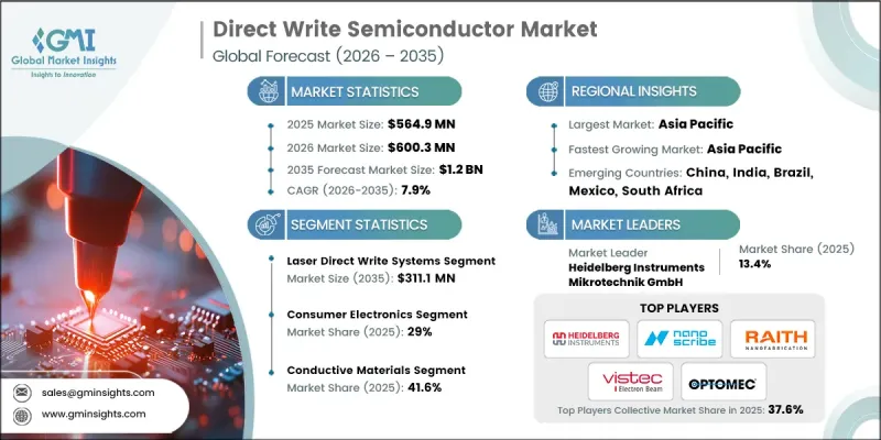
直接写入式半导体产业的成长主要源自于对速度更快、精度更高、成本效益更高的半导体製造技术日益增长的需求。随着製造商寻求能够降低製造复杂性并提高设计柔软性的替代方案,直接写入式技术正蓬勃发展。无掩模光刻和先进的图形化解决方案在这项变革中发挥核心作用,它们缩短了装置开发週期并提高了製造精度。这些技术有助于半导体开发商加速原型製作流程、最大限度地减少材料损耗并提高製造工作流程的效率。此外,随着向下一代电子设备的过渡不断推进,市场对能够支援紧凑型多功能组件设计的製造解决方案的需求也日益强劲。直接写入式技术使製造商能够以高精度沉积导电材料和半导体材料,从而开发出具有卓越分辨率的复杂电路。这种能力也使研究人员和製造商能够探索新的装置架构和创新设计方案。直接写入式半导体市场也受惠于混合製造方法的日益普及,这些方法将直接写入式製程与传统半导体製造技术结合。此类方法使製造商能够创建具有增强功能的高度客製化的多层电子元件。此外,人们对按需製造和小批量生产的兴趣日益浓厚,推动了直接写入技术在研究环境和专业电子产品开发中的应用。
| 市场范围 | |
|---|---|
| 开始年份 | 2025 |
| 预测期 | 2026-2035 |
| 上市时的市场规模 | 5.649亿美元 |
| 预测金额 | 12亿美元 |
| 复合年增长率 | 7.9% |
预计2035年,雷射直接照明系统市场规模将达到3.111亿美元。基于雷射的直接照明系统因其卓越的精度、高速的处理能力和多样化的图形化能力而备受关注。这些系统使製造商能够在微尺度上创建复杂的电路结构,而无需依赖传统的掩模製造技术。直接在基板上产生复杂图案的能力极大地提高了生产的柔软性并缩短了开发週期。基于雷射的直接照明解决方案在先进电子製造领域尤其重要,因为它们支援快速原型製作,并允许在开发阶段频繁地进行设计变更。
预计到2025年,导电材料市占率将达到41.6%,这反映了其在整个产业生态系统中的重要地位。导电材料在建构高精度电路和互连结构方面发挥着至关重要的作用,而这些结构对于现代电子元件至关重要。它们卓越的电气性能、对各种基板的适应性以及与直接写入製程的兼容性,使其成为从事先进微电子应用的製造商的理想选择。随着对高性能电子系统的关注度不断提高,对能够支援稳定可靠电路路径的导电材料的需求也日益增长。此外,这些材料非常适合扩展直接写入製造工艺,因为它们能够支援高效的电流传输并降低电阻。
预计2025年,欧洲直下式半导体市场规模将达9,640万美元。随着各地区政府日益重视提升国内半导体製造能力,欧洲直下式半导体产业正蓬勃发展。政策主导的措施正在促进技术创新,并支持整个全部区域先进半导体生产基础设施的扩张。产业相关人员、研究机构和政府机构之间的策略合作也推动了下一代半导体製造技术的发展。这些努力旨在提高供应链韧性,增强技术竞争力,并支持半导体生态系统的长期成长。因此,先进的图形化和积层製造技术的应用正在逐步扩展,从而巩固了该地区在不断发展的直下式半导体市场中的地位。
目录
第一章:调查方法和范围
第二章执行摘要
第三章业界考察
- 生态系分析
- 供应商情况
- 利润率分析
- 成本结构
- 每个阶段增加的价值
- 影响价值链的因素
- 中断
- 影响产业的因素
- 促进因素
- 对先进客製化半导体解决方案的需求日益增长
- 拓展柔性、穿戴式和印刷电子产品的应用领域。
- 对快速原型製作和缩短产品上市时间的要求。
- 增材製造及其与先进材料的集成
- 用于半导体封装的无掩模微影术技术取得进展
- 产业潜在风险与挑战
- 较高的初始资本投资和设备成本
- 直接写作过程的标准化程度有限。
- 市场机会
- 采用异质整合和系统级封装(SIP)
- 人工智慧驱动的流程优化和自动化
- 促进因素
- 监理情势
- 北美洲
- 欧洲
- 亚太地区
- 拉丁美洲
- 中东和非洲
- 波特五力分析
- PESTEL 分析
- 科技与创新趋势
- 当前技术趋势
- 新兴技术
- 新兴经营模式
- 合规要求
- 专利和智慧财产权分析
- 地缘政治和贸易趋势
第四章 竞争情势
- 介绍
- 企业市占率分析
- 按地区
- 北美洲
- 欧洲
- 亚太地区
- 拉丁美洲
- 中东和非洲
- 按地区
- 主要企业的竞争标竿分析
- 财务绩效比较
- 销售量
- 利润率
- 研究与开发
- 产品系列比较
- 产品线宽度
- 科技
- 创新
- 区域扩张比较
- 全球扩张分析
- 服务网路覆盖
- 按地区分類的市场渗透率
- 竞争定位矩阵
- 领导者
- 挑战者
- 追踪者
- 小众玩家
- 战略展望矩阵
- 财务绩效比较
- 2021-2024 年重大发展
- 併购
- 伙伴关係和联盟
- 技术进步
- 业务拓展与投资策略
- 数位转型计划
- 新兴/Start-Ups竞争对手的发展趋势
第五章 市场估算与预测:依技术/设备类型划分,2022-2035年
- 材料沉积系统
- 低黏度喷墨系统
- 中等黏度气溶胶喷射系统
- 高黏度微量点胶系统
- 雷射直接光刻系统
- 空间灯光调变器(基于SLM/DMD)
- 直接雷射扫描系统
- 双光子聚合系统
- 电子束直接微影系统
- 热扫描探测器微影术系统
第六章 市场估算与预测:依材料类型划分,2022-2035年
- 导电材料
- 半导体材料
- 介电和绝缘材料
- 功能复合材料
第七章 市场估计与预测:依基板,2022-2035年
- 软式电路板
- 刚性基板
- 保形/3D 基板
第八章 市场估计与预测:依应用领域划分,2022-2035年
- 先进的封装与互连技术
- 柔性印刷电子
- 微机电系统和感测器
- 天线和射频组件
- 生物医学和医疗保健设备
- 其他的
第九章 市场估计与预测:依最终用户产业划分,2022-2035年
- 航太/国防
- 车
- 家用电子电器
- 医疗保健和医疗设备
- 通信/5G
- 其他的
第十章 市场估价与预测:依地区划分,2022-2035年
- 北美洲
- 我们
- 加拿大
- 欧洲
- 德国
- 英国
- 法国
- 西班牙
- 义大利
- 荷兰
- 亚太地区
- 中国
- 印度
- 日本
- 澳洲
- 韩国
- 拉丁美洲
- 巴西
- 墨西哥
- 阿根廷
- 中东和非洲
- 南非
- 沙乌地阿拉伯
- 阿拉伯聯合大公国
第十一章:公司简介
- 主要企业
- Raith GmbH
- Heidelberg Instruments Mikrotechnik GmbH
- JEOL Ltd.
- Optomec Inc.
- 按地区分類的主要企业
- 北美洲
- NanoSystem Solutions, Inc.
- SVG Optronics Co., Ltd
- Nanoscribe GmbH &Co. KG
- 欧洲
- Vistec Electron Beam GmbH
- SUSS MicroTec SE
- Eulitha AG
- 亚太地区
- Elionix Inc.
- Crestec Corporation
- HTL Co. Japan Ltd.
- 北美洲
- 特殊玩家/干扰者
- KLOE SAS
- Holmarc Opto-Mechatronics Ltd.
- Microlight3D SAS
The Global Direct Write Semiconductor Market was valued at USD 564.9 million in 2025 and is estimated to grow at a CAGR of 7.9% to reach USD 1.2 billion by 2035.
Growth in the direct write semiconductor industry is largely driven by the increasing requirement for faster, highly accurate, and cost-efficient semiconductor manufacturing technologies. Direct write techniques are gaining momentum as manufacturers seek alternatives that improve design flexibility while reducing production complexity. Maskless lithography and advanced patterning solutions are playing a central role in this transformation by enabling faster device development cycles and improving manufacturing precision. These technologies help semiconductor developers accelerate prototyping processes, minimize material losses, and enhance the efficiency of fabrication workflows. In addition, the increasing shift toward next-generation electronic devices is creating a strong demand for manufacturing solutions capable of supporting compact and multifunctional component designs. Direct writing technology allows manufacturers to deposit conductive and semiconductive materials with high accuracy, enabling the development of complex circuits with superior resolution. This capability also allows researchers and manufacturers to explore new device architectures and innovative design possibilities. The direct write semiconductor market is also benefiting from the rising adoption of hybrid fabrication approaches that combine direct writing processes with traditional semiconductor production methods. Such approaches enable manufacturers to create highly customized and multi-layer electronic components with improved functionality. Furthermore, the increasing focus on on-demand manufacturing and limited-volume production is supporting the adoption of direct write technologies in research environments and specialized electronics development.
| Market Scope | |
|---|---|
| Start Year | 2025 |
| Forecast Year | 2026-2035 |
| Start Value | $564.9 Million |
| Forecast Value | $1.2 Billion |
| CAGR | 7.9% |
The laser direct write systems segment is projected to reach USD 311.1 million by 2035. Laser-based direct writing systems are gaining considerable attention due to their ability to deliver exceptional accuracy, high processing speed, and versatile patterning capabilities. These systems allow manufacturers to create intricate circuit structures at microscales without relying on conventional mask-based fabrication techniques. The ability to generate complex patterns directly on substrates significantly improves production flexibility and shortens development timelines. Laser-enabled direct writing solutions are particularly valuable in advanced electronics manufacturing because they support rapid prototyping and enable frequent design modifications during development stages.
The conductive materials segment accounted for 41.6% share in 2025, reflecting its significant importance within the overall industry ecosystem. Conductive materials play a vital role in the formation of high-precision circuits and interconnect structures that are essential for modern electronic components. Their strong electrical performance, adaptability across different substrate materials, and compatibility with direct writing processes make them a preferred choice for manufacturers working on advanced microelectronic applications. The increasing focus on high-performance electronic systems is further strengthening demand for conductive materials capable of supporting stable and reliable electrical pathways. In addition, the ability of these materials to support efficient current transmission and reduce electrical resistance makes them highly suitable for scaling direct write fabrication processes.
Europe Direct Write Semiconductor Market generated USD 96.4 million in 2025. The Europe direct write semiconductor industry is progressing as regional authorities place increasing emphasis on strengthening domestic semiconductor manufacturing capabilities. Policy-driven initiatives are encouraging technological innovation and supporting the expansion of advanced semiconductor production infrastructure across the region. Strategic collaboration among industry participants, research organizations, and government institutions is also contributing to the development of next-generation semiconductor fabrication technologies. These efforts are focused on improving supply chain resilience, enhancing technological competitiveness, and supporting long-term growth within the semiconductor ecosystem. As a result, the adoption of advanced patterning and additive manufacturing technologies is gradually expanding, reinforcing the region's role in the evolving direct write semiconductor market.
Key companies operating in the Global Direct Write Semiconductor Market include Raith GmbH, Vistec Electron Beam GmbH, Heidelberg Instruments Mikrotechnik GmbH, JEOL Ltd., Elionix Inc., SUSS MicroTec SE, Nanoscribe GmbH & Co. KG, Eulitha AG, Crestec Corporation, KLOE SAS, Holmarc Opto-Mechatronics Ltd., and HTL Co. Japan Ltd., Microlight3D SAS, NanoSystem Solutions, Inc., SVG Optronics Co., Ltd, and Optomec Inc. Companies active in the Global Direct Write Semiconductor Market are adopting several strategic initiatives to strengthen their competitive position and expand their technological capabilities. Many firms are increasing investment in research and development to enhance the precision, speed, and efficiency of direct writing technologies. Product innovation is another key strategy, with companies focusing on the development of advanced systems capable of supporting high-resolution semiconductor fabrication and complex circuit patterning. Strategic partnerships with research institutions and semiconductor manufacturers are also becoming more common as companies aim to accelerate technology development and expand commercial applications. Additionally, market participants are emphasizing the integration of advanced materials and software-driven design tools to improve system performance.
Table of Contents
Chapter 1 Methodology and Scope
- 1.1 Market scope and definition
- 1.2 Research design
- 1.2.1 Research approach
- 1.2.2 Data collection methods
- 1.3 Data mining sources
- 1.3.1 Global
- 1.3.2 Regional/Country
- 1.4 Base estimates and calculations
- 1.4.1 Base year calculation
- 1.4.2 Key trends for market estimation
- 1.5 Primary research and validation
- 1.5.1 Primary sources
- 1.6 Forecast model
- 1.7 Research assumptions and limitations
Chapter 2 Executive Summary
- 2.1 Industry 360° synopsis, 2021 - 2034
- 2.2 Key market trends
- 2.2.1 Technology/equipment type trends
- 2.2.2 Material type trends
- 2.2.3 Substrate trends
- 2.2.4 Application trends
- 2.2.5 End-user industry trends
- 2.2.6 Regional trends
- 2.3 TAM analysis, 2025-2034
- 2.4 CXO perspectives: Strategic imperatives
- 2.4.1 Executive decision points
- 2.4.2 Critical success factors
- 2.5 Future outlook and strategic recommendations
Chapter 3 Industry Insights
- 3.1 Industry ecosystem analysis
- 3.1.1 Supplier landscape
- 3.1.2 Profit margin analysis
- 3.1.3 Cost structure
- 3.1.4 Value addition at each stage
- 3.1.5 Factor affecting the value chain
- 3.1.6 Disruptions
- 3.2 Industry impact forces
- 3.2.1 Growth drivers
- 3.2.1.1 Increasing demand for advanced and custom semiconductor solutions
- 3.2.1.2 Expansion of flexible, wearable, and printed electronics applications
- 3.2.1.3 Rapid prototyping and reduced time-to-market requirements
- 3.2.1.4 Integration with additive manufacturing and advanced materials
- 3.2.1.5 Advancement in maskless lithography technologies for semiconductor packaging
- 3.2.2 Industry pitfalls and challenges
- 3.2.2.1 High initial capital expenditure and equipment costs
- 3.2.2.2 Limited standardization of direct writing processes
- 3.2.3 Market opportunities
- 3.2.3.1 Adoption in heterogeneous integration and system-in-package (SIP)
- 3.2.3.2 AI-enabled process optimization and automation
- 3.2.1 Growth drivers
- 3.3 Regulatory landscape
- 3.3.1 North America
- 3.3.2 Europe
- 3.3.3 Asia Pacific
- 3.3.4 Latin America
- 3.3.5 Middle East & Africa
- 3.4 Porter's analysis
- 3.5 PESTEL analysis
- 3.6 Technology and innovation landscape
- 3.6.1 Current technological trends
- 3.6.2 Emerging technologies
- 3.7 Emerging business models
- 3.8 Compliance requirements
- 3.9 Patent and IP analysis
- 3.10 Geopolitical and trade dynamics
Chapter 4 Competitive Landscape, 2024
- 4.1 Introduction
- 4.2 Company market share analysis
- 4.2.1 By region
- 4.2.1.1 North America
- 4.2.1.2 Europe
- 4.2.1.3 Asia Pacific
- 4.2.1.4 Latin America
- 4.2.1.5 Middle East & Africa
- 4.2.1 By region
- 4.3 Competitive benchmarking of key players
- 4.3.1 Financial performance comparison
- 4.3.1.1 Revenue
- 4.3.1.2 Profit margin
- 4.3.1.3 R&D
- 4.3.2 Product portfolio comparison
- 4.3.2.1 Product range breadth
- 4.3.2.2 Technology
- 4.3.2.3 Innovation
- 4.3.3 Geographic presence comparison
- 4.3.3.1 Global footprint analysis
- 4.3.3.2 Service network coverage
- 4.3.3.3 Market penetration by region
- 4.3.4 Competitive positioning matrix
- 4.3.4.1 Leaders
- 4.3.4.2 Challengers
- 4.3.4.3 Followers
- 4.3.4.4 Niche players
- 4.3.5 Strategic outlook matrix
- 4.3.1 Financial performance comparison
- 4.4 Key developments, 2021-2024
- 4.4.1 Mergers and acquisitions
- 4.4.2 Partnerships and collaborations
- 4.4.3 Technological advancements
- 4.4.4 Expansion and investment strategies
- 4.4.5 Digital transformation initiatives
- 4.5 Emerging/ startup competitors landscape
Chapter 5 Market Estimates and Forecast, By Technology / Equipment Type, 2022 - 2035 ($ Mn)
- 5.1 Key trends
- 5.2 Material deposition systems
- 5.2.1 Low-viscosity inkjet systems
- 5.2.2 Medium-viscosity aerosol jet systems
- 5.2.3 High-viscosity micro-dispensing systems
- 5.3 Laser direct write systems
- 5.3.1 Spatial light modulator (SLM/DMD-Based)
- 5.3.2 Direct laser scanning systems
- 5.3.3 Two-photon polymerization systems
- 5.4 Electron beam direct write systems
- 5.5 Thermal scanning probe lithography systems
Chapter 6 Market Estimates and Forecast, By Material Type, 2022 - 2035 ($ Mn)
- 6.1 Key trends
- 6.2 Conductive materials
- 6.3 Semiconductor materials
- 6.4 Dielectric & insulating materials
- 6.5 Functional composite materials
Chapter 7 Market Estimates and Forecast, By Substrate, 2022 - 2035 ($ Mn)
- 7.1 Key trends
- 7.2 Flexible substrates
- 7.3 Rigid substrates
- 7.4 Conformal/3D substrates
Chapter 8 Market Estimates and Forecast, By Application, 2022 - 2035 ($ Mn)
- 8.1 Key trends
- 8.2 Advanced packaging & interconnects
- 8.3 Flexible & printed electronics
- 8.4 Mems & sensors
- 8.5 Antennas & RF components
- 8.6 Biomedical & healthcare devices
- 8.7 Others
Chapter 9 Market Estimates and Forecast, By End-User Industry, 2022 - 2035 ($ Mn)
- 9.1 Key trends
- 9.2 Aerospace & defense
- 9.3 Automotive
- 9.4 Consumer electronics
- 9.5 Healthcare & medical devices
- 9.6 Telecommunications & 5G
- 9.7 Others
Chapter 10 Market Estimates and Forecast, By Region, 2022 - 2035 ($ Mn)
- 10.1 Key trends
- 10.2 North America
- 10.2.1 U.S.
- 10.2.2 Canada
- 10.3 Europe
- 10.3.1 Germany
- 10.3.2 UK
- 10.3.3 France
- 10.3.4 Spain
- 10.3.5 Italy
- 10.3.6 Netherlands
- 10.4 Asia Pacific
- 10.4.1 China
- 10.4.2 India
- 10.4.3 Japan
- 10.4.4 Australia
- 10.4.5 South Korea
- 10.5 Latin America
- 10.5.1 Brazil
- 10.5.2 Mexico
- 10.5.3 Argentina
- 10.6 Middle East and Africa
- 10.6.1 South Africa
- 10.6.2 Saudi Arabia
- 10.6.3 UAE
Chapter 11 Company Profiles
- 11.1 Global Key Players
- 11.1.1 Raith GmbH
- 11.1.2 Heidelberg Instruments Mikrotechnik GmbH
- 11.1.3 JEOL Ltd.
- 11.1.4 Optomec Inc.
- 11.2 Regional Key Players
- 11.2.1 North America
- 11.2.1.1 NanoSystem Solutions, Inc.
- 11.2.1.2 SVG Optronics Co., Ltd
- 11.2.1.3 Nanoscribe GmbH & Co. KG
- 11.2.2 Europe
- 11.2.2.1 Vistec Electron Beam GmbH
- 11.2.2.2 SUSS MicroTec SE
- 11.2.2.3 Eulitha AG
- 11.2.3 APAC
- 11.2.3.1 Elionix Inc.
- 11.2.3.2 Crestec Corporation
- 11.2.3.3 HTL Co. Japan Ltd.
- 11.2.1 North America
- 11.3 Niche Players / Disruptors
- 11.3.1 KLOE SAS
- 11.3.2 Holmarc Opto-Mechatronics Ltd.
- 11.3.3 Microlight3D SAS
 人工智慧半导体设计市场预测至2034年—按组件、设计阶段、技术、部署模式、应用和地区分類的全球分析
 IC逆向工程市场:依IC类型、方法、最终用户和应用划分-2026-2032年全球市场预测
 光敏三极管市场报告:趋势、预测与竞争分析(至2035年)导线架市场:2026-2032年全球市场预测(依材料、层结构、製程、引线数量、布线方式、板材覆盖率、应用和最终用户划分)半导体二极体市场:按类型、封装、材料、销售管道、额定电压、额定电流、应用和最终用户产业划分-2026-2032年全球市场预测
 2026年全球主动半导体盘式雷射市场报告半导体排气系统市场:依排气技术、组件、晶圆尺寸、应用、最终用户、安装类型和销售管道-全球预测,2026-2032年自动化FOUP开启器市场:依晶圆尺寸、类型、自动化程度、连接方式和最终用户产业划分-2026-2032年全球预测高纯度介质供应系统市场:依介质类型、纯度等级、销售管道和应用划分-全球预测,2026-2032年
 用于替代能源技术的半导体:机会和市场