


|
市场调查报告书
商品编码
1868994
物联网半导体设计与製造生态系统市场:2025-2030IoT Semiconductor Design and Manufacturing Ecosystem Market Report 2025-2030 |
|||||||
本报告详细分析了物联网半导体设计与製造生态系统,包括市场规模、关键趋势和市场占有率,涵盖电子设计自动化 (EDA) 和半导体智慧财产权 (IP) 市场以及代工(製造)市场。
范例预览
全球物联网设备的安装数量持续成长,每个设备内部的半导体密度也随之提高。这项需求成长是由复杂的物联网半导体价值链驱动的,负责底层晶片的设计和製造。
本报告对物联网半导体价值链进行了系统分析,重点在于设计和製造生态系统。其主要目标是透过定义、评估和分析价值链的三个基础(EDA、半导体IP和代工厂),帮助读者更好地理解这一领域。
报告摘要
报告概述
- 148页报告: 全面分析物联网半导体价值链,重点在于关于设计、IP 和製造生态系统。
- 三大技术深度分析: 对 EDA、半导体 IP 和代工厂的详细分析。
- 五大半导体宏观趋势: 分析影响物联网半导体价值链的宏观趋势,包括人工智慧、国家安全和地缘政治。
- 供应商市场占有率分析: 区隔 EDA、IP 和代工厂领域的竞争格局。
- 市场规模与预测: 分析物联网 EDA、IP 与代工厂市场,预测至 2030 年。
主要分析领域
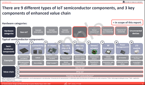
- 物联网半导体概述: 定义了九类半导体组件,并描述了本报告分析的物联网半导体价值链的三大主要部分。
- 物联网半导体市场概况: 提供物联网半导体组件的市场支出状况,以及设计与製造价值链的市场支出分析。此外,也概述了影响市场动态的五大跨产业趋势。
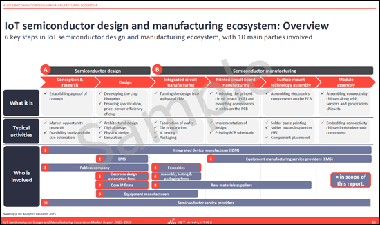
- 物联网半导体价值链概览: 描绘了设计和製造生态系统中的六个关键步骤和十个主要利害关係人群体。探讨了四大关键技术趋势,包括依区隔市场和地区划分的市场支出。
- 物联网EDA深度分析: 考察晶片设计和验证流程,从系统规格到製造和测试。提供区域支出分析、市场占有率、主要供应商概况以及四大新兴趋势。
- 物联网IP深度分析: 涵盖四大主要半导体IP类别(处理器、介面、记忆体和安全)及其区隔市场。包括区域市场规模、竞争格局评估和主要供应商概况。
- 物联网晶圆代工深度解析:概述半导体製造流程(晶圆製备、製造、组装、测试和封装的演变)。内容包括区域支出、市场占有率分析以及领先晶圆代工厂的概况。
公司列表:
|
|
|
目录
第一章:摘要整理
第二章:引言
- 章节概述
- 出发点:物联网设备的数量持续成长,预计到2030年将达到390亿。
- 每个设备内部的半导体密度也不断增加。
- 物联网半导体元件共有九种类型,其中增强型价值链包含三种关键元件。
- 定义:半导体和物联网半导体
- 定义:处理器
- 定义:连接晶片组
- 定义:人工智慧晶片组
- 定义:安全晶片组
- 定义:其他
第三章 概览:物联网半导体市场
- 章节概述
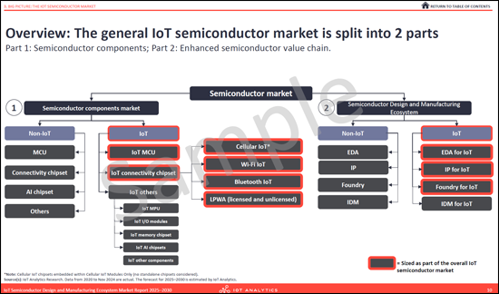
- 概述:物联网半导体市场分为两部分
- 第一部分:物联网半导体元件 - 依类型划分的支出
- 第二部分:物联网半导体设计与製造生态系统 - 依区隔市场划分的支出
- 物联网半导体整体竞争格局
- 物联网区隔市场对多家半导体公司的重要性
- 影响物联网半导体的五大趋势
- 近期发表的新半导体产品晶圆厂
- 研究方法:物联网相关业务概况 - 台积电
物联网半导体设计与製造生态系:概论
- 章节概述
- 物联网半导体设计与製造生态系:概述
- 物联网半导体设计与製造生态系:定义
- 物联网半导体设计与製造市场支出 - 概述
- 物联网半导体设计与製造分析师评论
- 物联网半导体设计与製造市场支出 - 依区隔市场划分
- 物联网半导体设计与製造市场支出 - 依地区划分
- 竞争格局:物联网半导体设计与製造生态系统中的主要供应商
- 趋势
第五章:物联网EDA
- 章节概述
- 物联网半导体设计:概述
- 晶片设计与验证
- 印刷电路板设计:製程概述
- 异质整合:概述
- 全球物联网EDA支出概况:2020-2030
- 分析师对物联网EDA的评论
- 全球物联网EDA支出预测 - 依地区划分:2020-2030
- 竞争格局:物联网EDA市场的主要供应商
- 物联网EDA竞争格局
- 主要公司简介:Cadence
- 主要公司简介:Synopsys
- 趋势
第六章 物联网IP
- 章节概述
- 物联网IP
- 全球物联网IP支出概况:2020-2030
- 分析师对物联网IP的评论
- 全球物联网IP支出(依地区划分): 2020-2030
- 竞争格局:物联网市场领先的IP供应商
- 物联网IP竞争格局
- 主要公司简介:Arm
第七章:物联网晶圆代工厂
- 章节概述
- 物联网晶片组半导体製造
- 全球物联网支出概况:晶圆代工厂:2020-2030
- 分析师对物联网晶圆代工厂的评论
- 全球物联网支出:晶圆代工厂 - 依地区划分:2020-2030
- 竞争格局:领先的物联网晶圆代工厂
- 物联网晶圆代工厂竞争格局
- 主要公司简介:台积电
第八章:研究方法与市场定义
第九章:物联网分析概论
A 148-page report detailing the IoT semiconductor design and manufacturing ecosystem, covering EDA and IP markets as well as foundries, with market sizing, key trends, and market shares.
Sample preview
The global installed base of connected IoT devices continues to expand, driving a corresponding increase in semiconductor density within each device. This growing demand is supported by a complex IoT semiconductor value chain responsible for designing and manufacturing the underlying chips.
This report provides a structured IoT semiconductor value chain analysis, focusing on the design and manufacturing ecosystem. Its primary objective is to help readers understand this landscape by defining, sizing, and analyzing the three foundational pillars of the value chain: Electronic Design Automation (EDA), Semiconductor Intellectual Property (IP), and Foundries.
The findings are based on extensive primary research, including interviews with semiconductor experts from leading vendors and end-user organizations across the IoT semiconductor value chain, complemented by secondary research and insights gathered from major industry trade fairs.
Sample preview
Report at a glance
- 148-page report: A comprehensive analysis of the IoT semiconductor value chain, focusing on the design, IP, and manufacturing ecosystem.
- 3 technology deep dives: In-depth analyses of Electronic Design Automation (EDA), Semiconductor Intellectual Property (IP), and Foundries for IoT.
- 5 overarching semiconductor trends: Examination of macro trends (e.g., AI, security, geopolitics) impacting the IoT semiconductor value chain.
- Vendor market share analysis: A breakdown of the competitive landscape for each of the three ecosystem segments (EDA, IP, and Foundries).
- Market sizing and forecast: Market analysis for the EDA, IP, and Foundry for IoT markets, with forecasts to 2030.
Key areas of analysis
- Introduction to IoT semiconductors: Defines nine categories of semiconductor components and explains the three key segments of the IoT semiconductor value chain analyzed in this report.
- Big picture-The IoT semiconductor market: Provides market spending analysis for both IoT semiconductor components and the design/manufacturing segments of the IoT semiconductor value chain. Also outlines five cross-industry trends influencing market dynamics.
- Overview of the IoT semiconductor value chain: Maps the six critical steps and ten primary stakeholder groups within the design and manufacturing ecosystem. Includes market spending by segment and region and explores four major technical trends.
- EDA for IoT deep dive: Examines the chip design and verification process from system specification to fabrication and testing. Provides regional spending analysis, market share insights, key vendor profiles, and four emerging trends.
- IP for IoT deep dive: Covers the four main types of semiconductor IP (Processor, Interface, Memory, and Security) and their sub-segments. Includes regional market sizing, competitive landscape assessment, and a leading vendor profile.
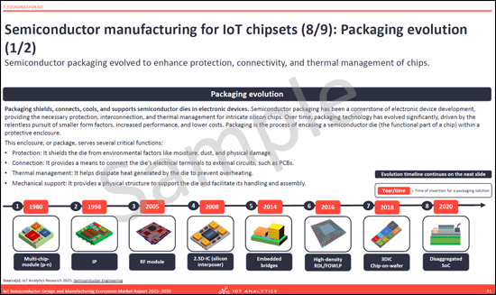
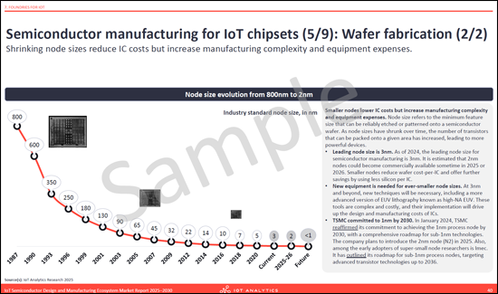
- Foundries for IoT deep dive: Outlines the semiconductor manufacturing process, including wafer preparation, fabrication, assembly, testing, and packaging evolution. Analyzes regional spending, market shares, and includes a leading foundry profile.
A data-driven foundation for key business functions
- Strategy and corporate development: Inform strategic planning with market sizing, 2030 forecasts, and analysis of macro trends impacting the IoT semiconductor value chain, such as geopolitical shifts and supply chain diversification.
- Product management and marketing: Guide product and technology roadmaps using detailed analyses of emerging technology trends and competitive dynamics across the EDA, IP, and foundry segments of the IoT semiconductor value chain.
- R&D and engineering leadership: Direct technical priorities with insights into EDA workflows, IP block architectures, and advanced packaging innovations, along with trends such as security-by-design and cloud-based design platforms.
- Market intelligence and competitive analysis: Benchmark market position within the IoT semiconductor value chain using granular market share data and vendor profiles for the EDA, IP, and foundry segments.
Key concepts defined
- IoT semiconductor value chain: The ecosystem of companies and processes involved in chip creation, defined in this report by six key stages: conception & research, design, integrated circuit manufacturing, printed circuit board manufacturing, surface mount technology assembly, and module assembly.
- Electronic design automation (EDA) for IoT: A key segment of the IoT semiconductor value chain providing software and tools used to design silicon or modules for IoT endpoints or gateways. Includes RTL design, simulation, verification, synthesis, analog/mixed-signal, DFT, advanced packaging, and PCB tools.
- Semiconductor intellectual property (IP) for IoT: A foundational segment of the IoT semiconductor value chain comprising licenses and royalties derived from integrating reusable IP blocks (IP cores) into silicon for IoT devices.
- Foundries for IoT: The manufacturing segment of the IoT semiconductor value chain that provides wafer fabrication and advanced packaging services for chips designed by fabless semiconductor companies.
- Chiplet: A small, specialized IC designed to interconnect with other chiplets or larger ICs. This modular structure enables integration of multiple chips using different process nodes within a single package.
- Heterogeneous integration: A manufacturing approach that combines multiple, separately manufactured components (chips, chiplets, etc.) into a single package, often using different materials and processes.
Questions answered:
- Which stakeholders are involved across EDA, IP, and foundry stages of the value chain?
- Which technologies are critical across EDA, IP, and foundries in enabling IoT semiconductor development?
- What is the current and projected market size of EDA, IP, and foundry for IoT markets?
- What is the market share of leading vendors across these three segments?
- What trends are shaping the future of the IoT semiconductor design and manufacturing ecosystem?
Companies mentioned:
A selection of companies mentioned in the report.
|
|
|
Table of Contents
1. Executive summary
2. Introduction
- Chapter overview: Introduction
- Starting point: The number of loT connected devices continues to grow - Expected to reach 39 billion by 2030
- The semiconductor density within each device also continues to increase
- There are 9 different types of IoT semiconductor components, and 3 key components of enhanced value chain.
- Definitions (1/6): Semiconductors & IoT semiconductors
- Definitions (2/6): Processors
- Definitions (3/6): Connectivity chipsets
- Definitions (4/6): AI chipsets
- Definitions (5/6): Security chipsets
- Definitions (6/6): Other key components
3. Big picture: The IoT semiconductor market
- Chapter overview: Big picture: The IoT semiconductor market
- Overview: The general IoT semiconductor market is split into 2 parts
- Part 1: IoT semiconductor components - Spending by type
- Part 2: IoT semiconductor design and manufacturing ecosystem - Spending by segment
- Overall IoT semiconductor competitive landscape
- Importance of IoT as a segment within several chip companies
- 5 overarching trends impacting IoT semiconductors
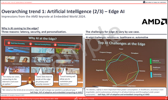
- Overarching trend 1
- Overarching trend 2
- Overarching trend 3
- Overarching trend 4
- Overarching trend 5
- Recent announcements for new semiconductor plants
- Methodology: Mapping IoT-related business - TSMC
IoT semiconductor design and manufacturing ecosystem: Overview
- Chapter overview: IoT semiconductor design and manufacturing ecosystem: Overview
- IoT semiconductor design and manufacturing ecosystem: Overview
- IoT semiconductor design and manufacturing ecosystem: Definitions
- IoT semiconductor design and manufacturing market spending - Overview
- Analyst commentary on the IoT semiconductor design and manufacturing
- IoT semiconductor design and manufacturing market spending - By segment
- IoT semiconductor design and manufacturing market spending - By region
- Competitive landscape: Key vendors in IoT semiconductor design and manufacturing ecosystem
- Trend 1
- Trend 2
- Trend 3
- Trend 4
5. EDA for IoT
- Chapter overview: EDA for IoT
- IoT semiconductor design: Overview
- Chip design and verification
- Printed circuit board design: Process overview
- Heterogeneous integration: Overview
- Global EDA for IoT spending 2020-2030 - Overview
- Analyst commentary on the EDA for IoT
- Global EDA for IoT spending 2020-2030 - By region
- Competitive landscape: Key vendors in EDA for IoT market
- EDA for IoT competitive landscape
- Key company profile: Cadence
- Key company profile: Synopsys
- Trend 1
- Trend 2
- Trend 3
- Trend 4
6. IP for IoT
- Chapter overview: IP for IoT
- IP for IoT
- Global IP for IoT spending 2020-2030 - Overview
- Analyst commentary on the IP for IoT
- Global IP for IoT spending 2020-2030 - By region
- Competitive landscape: Key vendors in IP for IoT market
- IP for IoT competitive landscape
- Key company profile: Arm
7. Foundries for IoT
- Chapter overview: Foundries for IoT
- Semiconductor manufacturing for IoT chipsets
- Global Foundry for IoT spending 2020-2030 - Overview
- Analyst commentary on the Foundries for IoT
- Global Foundry for IoT spending 2020-2030 - By region
- Competitive landscape: Key foundries for IoT
- Foundries for IoT competitive landscape
- Key company profile: TSMC
8. Methodology & market definitions
- Key market definitions
- Country mappings to regions
- Research Methodology
9. About IoT Analytics
 2026年全球半导体设计市场报告2026年全球有机半导体市场报告
 人工智慧半导体设计市场预测至2034年—按组件、设计阶段、技术、部署模式、应用和地区分類的全球分析
 IC逆向工程市场:依IC类型、方法、最终用户和应用划分-2026-2032年全球市场预测
 用于替代能源技术的半导体:机会和市场
 光敏三极管市场报告:趋势、预测与竞争分析(至2035年)导线架市场:2026-2032年全球市场预测(依材料、层结构、製程、引线数量、布线方式、板材覆盖率、应用和最终用户划分)半导体二极体市场:按类型、封装、材料、销售管道、额定电压、额定电流、应用和最终用户产业划分-2026-2032年全球市场预测2026年全球主动半导体盘式雷射市场报告半导体排气系统市场:依排气技术、组件、晶圆尺寸、应用、最终用户、安装类型和销售管道-全球预测,2026-2032年