|
市场调查报告书
商品编码
1548963
混合加入:专利格局分析(2024)Hybrid Bonding - Patent Landscape Analysis 2024 |
|||||||
主要功能
- 70+ PDF 投影片
- Excel 文件:1,600 多 专利族
- 全球专利趋势:专利公布、专利申请国家等的时间趋势。
- 每个细分市场的主要专利权人和新进者。
- 主要公司的智慧财产权地位及其专利组合的相对实力。
- 依发明类型(製造方法、装置、半导体结构和装置)和目标应用(影像感测器、2.5D/3D IC、3D 堆迭记忆体、光子学等)分类的专利。
- 主要公司的智慧财产权概况(专利组合概览、技术覆盖范围、地理覆盖范围、关键专利、近期智慧财产权活动等)
- 包含报告中分析的所有专利的 Excel 资料库(专利分类、更新线上资料库的超连结、受让人从统计分析中获得的所有资料)。
在决定半导体封装未来的尖端键结技术的全球 IP 竞争市场中,谁是主要参与者和新进者?
混合键结是先进封装的关键
混合键结结合了电介质对电介质键合和金属对金属键合,可在不使用焊料或其他黏合剂的情况下互连晶圆到晶圆、晶片到晶圆以及晶片到晶片。这种键合技术用于多个晶片的垂直堆迭,允许在一个封装内实现具有各种功能(逻辑、记忆体、类比、感测器等)的不同类型晶片的 3D 异构整合和互通性。混合结可实现细间距(小于10微米,甚至小于1微米),这在互连密度和装置性能方面具有显着优势。金属与金属的直接接触可促进高效散热并减少寄生延迟。由于电介质使每个金属焊盘绝缘,因此焊盘之间不存在讯号干扰。
混合键结技术于 2005 年随着 Ziptronix 的 DBI-R(直接键结互连)技术的推出而出现。 2015年,Tessera(现为Adeia)收购了Ziptronix,DBI-R技术于2016年透过索尼的CMOS影像感测器(CIS)进入市场,该技术应用于三星Galaxy S7手机。从那时起,混合键合技术在记忆体、逻辑、射频和光子学等各种应用中得到了探索,现在被半导体行业的更多公司采用。
在过去五年中,混合键结技术已成为先进半导体封装的关键推动因素,导致专利活动增加和竞争性智??慧财产权 (IP) 格局的重大演变。主要专利持有者正在加强在美国、中国和欧洲的智慧财产权地位,同时各种新公司正在进入专利领域。目前,对于半导体封装产业的企业来说,从智慧财产权的角度审视混合键结技术极为重要。
在此背景下,Knowmade 正在分析新的专利格局,重点在于使用混合键合製程和混合键结互连的半导体装置。从 1,600 多个专利族(发明)中提取了 5,800 多项专利。本报告的目的是深入了解当前的智慧财产权活动、领先的智慧财产权公司的地位、其专利的目标开发领域以及其专利组合如何支持其市场策略。
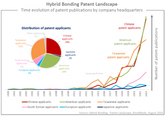
主要趋势、主要企业智慧财产权地位及智慧财产权策略分析
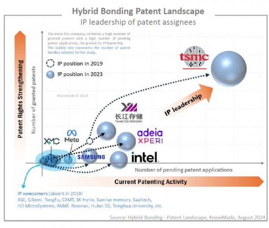
透过专利分析,我们解释智慧财产权 (IP) 公司的地位,揭示加强其智慧财产权组合的策略,强调其限制其他公司的专利活动和营运自由的能力,并识别有前途的新公司。未来的知识产权领导者。 IP 竞争分析必须反映具有进入和扩展先进半导体封装市场策略的公司的愿景。本报告全面概??述了竞争性智慧财产权格局以及与混合键结技术相关的最新技术发展。该报告涵盖智慧财产权动态和主要趋势,包括专利申请、专利受让人、申请国家、专利技术和涵盖的申请。我们还确定了知识产权领导者和最活跃的专利申请人,并重点关注该领域的未知公司和新进入者。
发明类型、目标申请、主要专利
专利涵盖了所要求的发明类型(混合结製造方法和介面工程、混合结技术设备、混合结半导体结构/装置)以及专利中提到的应用(影像感测器、2.5D/3D IC、 3D 堆迭记忆体、光子学、MEMS、RF 等)。目前,2.5D/3D IC 领域正在推动专利活动,但与光子学、micro-LED、MEMS 和 RF 等其他活动相关的专利正在迅速增加。
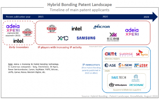
动态智慧财产权格局:领先公司地位的演变与新专利申请人的进入
台积电、Adeia、长江储存、英特尔、三星引领专利情势,活跃专利活动,扩大主要国家的发明保护。 Adeia 是 DBI-R 技术的先驱和所有者,采取了积极的策略,向索尼、长江存储、美光和 Kioxia 等多家半导体公司申请专利并将其混合结 IP 组合授权。儘管该公司拥有强大的智慧财产权地位,但其他公司正在开发自己的混合黏合专利组合。近年来,越来越多的记忆体製造商涉足IP环境(CXMT、SK Hynix、Sunrise Memory),OSAT和设备/材料供应商也进入IP领域(ASE、TongFu、SJSemi、Applied Materials)。 。本报告概述了主要公司持有的智慧财产权组合,并描述了他们的关键专利和最近的智慧财产权活动。此外,我们也涵盖主要智慧财产权合作(共同拥有专利、智慧财产权转让、授权协议)和专利诉讼。
有用的 Excel 专利资料库
报告包括专利资讯(编号、日期、受让人、标题、摘要等)、更新线上资料库的超连结(文字、法律状态等)、隶属关係部分(製造方法、设备、包含广泛的 Excel包含本报告分析的所有专利(包括半导体装置、影像感测器、2.5D/3D IC、3D堆迭记忆体等)和关键专利的资料库。此外,Excel 文件还包含受让人从统计分析中获得的完整信息,包括专利族数量、专利活动时间表、已授权和待审专利数量以及专利组合的区域分析数据。
本报告提及的企业 (部分)
TSMC,YMTC,Xperi/Adeia,Intel,Samsung,XMC,Micron,Tongfu Microelectronics,ASE,Meta (Facebook),Nanya Technology,CXMT,Huawei,Onsemi,OmniVision,AMD,ICLeague Technology,Monolithic 3D,UMC/Wavetek,Qualcomm,SJSemi,Saultech,SK Hynix,Tsinghua University,CEA,imec,Galaxycore Microelectronics,Apple,EVG,HD MicroSystems,NCAP,STMicroelectronics,Applied Materials,Resonac,GlobalFoundries,SunRise Memory,阿里巴巴 Group,AP Memory,SMIC,Powerchip Semiconductor Manufacturing,MICLEDI,AMS-Osram,SmartSens Technology,深圳 Aoshiwei Technology,MediaTek,IBM,RTX Corporation,pSemi,Winbond electronics,Sony,NVIDIA,Haiguang Information Technology,Shanghai Huali Integrated Circuit Manufacturing,JCET Group,SEMES,Tectus Group,Hanmi,Western Digital,Shibaura Mechatronics,宁波 Semiconductor International Corporation (NSI),HIDM - Huaian Imaging Device Manufacturer,Bruker,Suzhou Ultiview Technology,KLA,Shanghai Fudan Microelectronics Group,Anhui Xinbiyou Information Technology,Tokyo Electron,Shanghai Yibu Semiconductor,HTSI,GROQ,Dixtech innovation,Qingdao New Core Technology,PsiQuantum,Canon,Infineon,Shanghai Biren Intelligent Technology,Yangtze River Advanced Storage Industry Innovation Center,G-ray Switzerland等。
目录
简介
摘要整理
Excel资料库
- 含由于从为了本报告被选择了的全部的专利和,统计分析被得了的受让人的完全的资料的Excel文件
专利形势概要
- 主要趋势和IP企业
- 专利出版数量的时间序列变化
- 主要专利权人
- 知识产权公司时间表
- 知识产权公司的主要类型
- 知识产权领域的新进入者
- 主要公司的专利:当前法律状况
- 专利权人的智慧财产权领先地位以及 2019 年以来的演变
- 主要公司专利的地理范围
- 主要的IP合作
- 共同所有IP
- IP转让
- 授权合约
- 专利的市场区隔
- 市场区隔定义
- 要求保护的发明类型:
- 混合连接製造流程和介面工程
- 混合键结设备
- 使用混合结互连製造的半导体结构/装置
- 目标用途
- 影像感测器(SPAD、CMOS影像感测器、光学感测器等)
- D/3D IC(任何类型 IC 晶片的组装(内存对内存除外))
- 3D堆迭记忆体(记忆体上的记忆体)
- 其他应用(射频、MEMS、光子学、LED 等)
- 专利出版数量趋势:按细分市场
- 主要专利权人:依细分市场划分
- 专利权人的智慧财产权领导力:每个细分市场
主要专利
- 从现有技术、智慧财产权风险和技术角度来看最重要的专利
- 主要专利属于的市场区隔
- 主要专利的所有者
发明专利权者选择的IP简介
- TSMC,Adeia/Xperi,TongFu,ASE
- 各企业相关:
- 专利组合概要 (IP动态,市场区隔,法律上的状态,企业发展地区等)
- 主要专利的说明
- 最近的专利申请的说明
专利诉讼
附录
KNOWMADE的简报
KEY FEATURES:
- PDF>70 slides
- Excel file>1,600 patent families
- Global patenting trends, including time evolution of patent publications, countries of patent filings, etc.
- Main patent assignees and IP newcomers in the different segments.
- Key players' IP position and the relative strength of their patent portfolio.
- Patents categorized by type of invention (manufacturing methods, equipment, semiconductor structures and devices) and targeted applications (image sensors, 2.5D/3D IC, 3D-stacked memories, photonics, etc.)
- IP profile of key players (patent portfolio overview, technical coverage, geographical coverage, key patents, recent IP activity, etc.)
- Excel database containing all patents analyzed in the report, including patent segmentations and hyperlinks to an updated online database, along with the complete data by assignee from the statistical analyses.
Who are the key players and newcomers in the global IP race for the most advanced bonding technology shaping the future of semiconductor packaging?
Hybrid bonding has become a key enabler of advanced packaging
Hybrid bonding combines dielectric-to-dielectric and metal-to-metal bonds to interconnect wafer-to-wafer, die-to-wafer, or die-to-die without the need for solder or other adhesives. This bonding technology is used for the vertical stacking of multiple chips, enabling 3D heterogeneous integration and interoperability of different types of chips with various functions (e.g., logic, memory, analog, sensors) within a single package. Hybrid bonding enables finer pitch (<10 micrometerm, or even <1 micrometerm) with significant benefits for interconnect density and device performance. The direct metal-to-metal contact facilitates efficient heat dissipation and reduces the parasitic delay. The dielectric insulates each metal pad so that there is no signal interference between the pads.
Hybrid bonding technology emerged in 2005 with the introduction of Ziptronix's direct bond interconnect (DBI-R) technology. In 2015, Tessera (now Adeia) acquired Ziptronix, and DBI-R technology entered the market in 2016 through Sony's CMOS image sensor (CIS) used in Samsung's Galaxy S7 mobile phone. Since then, hybrid bonding technology has been explored for various applications, including memory, logic, RF, and photonics, and it is now being adopted by more companies across the semiconductor industry.
Over the past five years, hybrid bonding technology has become a key enabler of advanced semiconductor packaging, leading to a strong increase in patenting activity and a significant evolution of the competitive intellectual property (IP) landscape. Major patent owners have strengthened their IP positions in the US, China, and Europe, while various new players have entered the patent landscape. It is now crucial for companies operating in the semiconductor packaging industry to closely examine hybrid bonding technology from an IP perspective.
In this context, Knowmade is releasing a new patent landscape report focusing on the hybrid bonding process and semiconductor devices made using hybrid bonding interconnects. Over 5,800 patents from more than 1,600 patent families (inventions) have been selected. This report aims to provide insights into current IP activities, the positions of key IP players, the applications they target in their patents, and how their patent portfolios can support their market strategies.

Understanding the main trends, the key players' IP position and IP strategy
Through patent analysis, we describe the position of IP players, unveil their strategies to strengthen their IP portfolio, highlight their capability to limit the patenting activity and freedom-to-operate of other firms, identify promising new players, and forecast what would be the future IP leaders. IP competition analysis should reflect the vision of players with a strategy to enter and develop their business in the advanced semiconductor packaging market. In this report, we provide a comprehensive overview of the competitive IP landscape and latest technological developments related to hybrid bonding technology. The report covers IP dynamics and key trends in terms of patents applications, patent assignees, filing countries, patented technologies, and targeted applications. It also identifies the IP leaders, most active patent applicants, and sheds light on under-the-radar companies and new players in this field.
Invention type, targeted applications, and key patents
The patents have been categorized according to the type of claimed invention (hybrid bonding manufacturing methods and interface engineering, equipment for hybrid bonding technology, hybrid bonded semiconductor structures or devices) and the applications mentioned in the patents (image sensors, 2.5D/3D ICs, 3D-stacked memories, photonics, MEMS, RF, etc.). The 2.5D/3D IC segment is currently driving patenting activity, while patents related to other applications, such as photonics, microLED, MEMS, and RF, have surged.

A dynamic IP landscape: evolution of leading players' positions and entry of new patent applicants
TSMC, Adeia, YMTC, Intel, and Samsung are leading the patent landscape, increasing patenting activity, and expanding invention protection in key countries. As pioneer and owner of DBI-R technology, Adeia has adopted an aggressive strategy to assert its patents and license its hybrid bonding IP portfolio to various semiconductor companies, including Sony, YMTC, Micron, and Kioxia. Despite its strong IP position, other players have been developing their own hybrid bonding patent portfolios. In recent years, more memory makers have become involved in the IP landscape (CXMT, SK Hynix, Sunrise Memory), and OSATs and equipment/materials suppliers have entered the IP arena (ASE, TongFu, SJSemi, Applied Materials, Saultech, HD MicroSystems). In this report, we provide an overview of the IP portfolios held by key players and describe key patents and recent IP activities. Additionally, we highlight the main IP collaborations (co-owned patents, IP transfers, licensing agreements) and patent litigations.

Useful Excel patent database
This report includes an extensive Excel database with all patents analyzed in this study, including patent information (numbers, dates, assignees, title, abstract, etc.) and hyperlinks to an updated online database (original documents, legal status, etc.), affiliation segments (manufacturing methods, equipment, semiconductor devices, image sensors, 2.5D/3D IC, 3D-stacked memory, etc.), and key patents. Additionally, the Excel file comprises the complete data by assignee from the statistical analyses, including the number of patent families, timeline of patenting activity, number of granted patents and pending patent applications, and geographical coverage of patent portfolio.
Companies mentioned in the report (non-exhaustive)
TSMC, YMTC, Xperi/Adeia, Intel, Samsung, XMC, Micron, Tongfu Microelectronics, ASE, Meta (Facebook), Nanya Technology, CXMT, Huawei, Onsemi, OmniVision, AMD, ICLeague Technology, Monolithic 3D, UMC/Wavetek, Qualcomm, SJSemi, Saultech, SK Hynix, Tsinghua University, CEA, imec, Galaxycore Microelectronics, Apple, EVG, HD MicroSystems, NCAP, STMicroelectronics, Applied Materials, Resonac, GlobalFoundries, SunRise Memory, Alibaba Group, AP Memory, SMIC, Powerchip Semiconductor Manufacturing, MICLEDI, AMS-Osram, SmartSens Technology, Shenzhen Aoshiwei Technology, MediaTek, IBM, RTX Corporation, pSemi, Winbond electronics, Sony, NVIDIA, Haiguang Information Technology, Shanghai Huali Integrated Circuit Manufacturing, JCET Group, SEMES, Tectus Group, Hanmi, Western Digital, Shibaura Mechatronics, Ningbo Semiconductor International Corporation (NSI), HIDM - Huaian Imaging Device Manufacturer, Bruker, Suzhou Ultiview Technology, KLA, Shanghai Fudan Microelectronics Group, Anhui Xinbiyou Information Technology, Tokyo Electron, Shanghai Yibu Semiconductor, HTSI, GROQ, Dixtech innovation, Qingdao New Core Technology, PsiQuantum, Canon, Infineon, Shanghai Biren Intelligent Technology, Yangtze River Advanced Storage Industry Innovation Center, G-ray Switzerland, and more.
TABLE OF CONTENTS
INTRODUCTION
- Context and objectives of the report
- Scope of the report
- Reading guide
- Excel database
EXECUTIVE SUMMARY
EXCEL DATABASE
- Excel file that includes all patent selected for this study, along with the
- complete data by assignee from the statistical analyses.
PATENT LANDSCAPE OVERVIEW
- Main trends and IP players
- Time evolution of patent publications
- Main patent assignees
- Timeline of IP players
- Typology of main IP players
- IP newcomers
- Current legal status of main players' patents
- IP leadership of patent assignees and evolution from 2019
- Geographical coverage of main players' patents
- Main IP collaborations
- Co-owned IP
- IP transfers
- Licensing agreements
- Patent segmentation
- Segments definition
- Type of claimed invention:
- Hybrid bonding manufacturing process and interface engineering
- Apparatus/Equipment for hybrid bonding
- Semiconductor structure or device made using hybrid bonding interconnects
- Targeted applications
- Image sensor (SPADs, CMOS image sensors, light sensing devices, etc.)
- 2.5D/3D IC (assembly of any type of IC dies, excluding memory-on-memory)
- 3D-stacked memory (memory-on-memory)
- Other applications (RF, MEMS, Photonics, LEDs, etc.)
- Time evolution of patent publication by segment
- Main patent assignees by segment
- IP leadership of patent assignees for each segment
KEY PATENTS
- Most important patents in terms of prior-art, IP risks and technology
- Segments to which key patents belong
- Owners of key patents
IP PROFILE OF A SELECTION OF PATENT ASSIGNEES
- TSMC, Adeia/Xperi, TongFu, ASE
- For each player:
- Patent portfolio overview (IP dynamics, segments, legal status, geographic coverage, etc.)
- Description of key patents
- Description of recent patent applications
PATENT LITIGATION
ANNEX
- Methodology for patent search, selection and analysis
- Methodology to identify key patents
- Terminology


