


 |
市场调查报告书
商品编码
1406092
半导体测量与检测设备:市场占有率分析、产业趋势、2024年至2029年成长预测Semiconductor Metrology And Inspection Equipment - Market Share Analysis, Industry Trends & Statistics, Growth Forecasts 2024 - 2029 |
||||||
※ 本网页内容可能与最新版本有所差异。详细情况请与我们联繫。
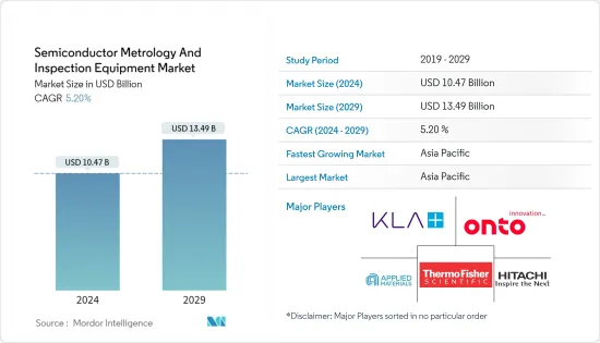
预计2024年半导体计量及检测设备市场规模为104.7亿美元,预计2029年将达到134.9亿美元,预测期间(2024-2029年)复合年增长率为5.20%。
主要亮点
- 半导体计量和检测对于管理半导体製造流程至关重要。半导体晶圆的製造过程大约涉及 400 到 600 个步骤,需要一到两个月的时间。如果在流程早期出现缺陷,那么流程后期所做的所有工作都将被浪费。在半导体製造过程的重要环节,有测量和检查过程来确认和维持特定的产量比率。
- 智慧型手机、家用电子电器和汽车应用等应用正在推动对高性能、低成本半导体材料的需求。无线技术(5G)和人工智慧等技术变革正在刺激这些产业。此外,物联网(IoT)设备的成长趋势预计将鼓励半导体产业投资该设备以实现智慧产品。
- 工业和住宅领域互联物连网型设备的日益普及趋势增加了对高性能半导体的需求,这反过来又为所研究市场的成长创造了良好的前景。据爱立信称,到2022年终,连接物联网技术NB-IoT和Cat-M的设备数量将达到近5亿。此外,宽频物联网 (4G/5G) 连线预计到 2022 年将达到 13 亿,到 2028 年约占所有蜂巢式物联网连线的 60%。
- 然而,高设置成本和缺乏处理测量系统的专业知识等因素预计将有效阻碍预测期内的市场成长。为了应对这些挑战,服务型企业正在按需提供计量服务,使他们能够在精密尺寸测量的专业领域提供专业的扩展。
- 此外,当前美国贸易争端等宏观经济因素也推动了研究市场,美国对中国实施了多项制裁,并阻止中国获得先进的半导体设备,这对成长构成挑战。由于中国是市场供应链的关键地区之一,这种趋势将阻碍市场的成长。
半导体测量和检测设备市场的趋势
晶圆检测取得显着成长
- 预计3D几年推动晶圆检测需求的主要因素之一将是需求的增加。 3D 电路在行动消费性电子产品、感测器、MEMS 和工业产品等多种空间受限的应用中变得越来越流行,因为它们提高了整体产品性能,包括速度、耐用性、更低的功耗和更轻的普及。
- 随着经济实惠的云端处理解决方案的广泛普及,随着企业和产业越来越多地使用伺服器和资料中心系统,微处理器和数位讯号处理器等逻辑装置变得越来越受欢迎,需求预计将增加。此外,随着越来越多的连接设备具有物联网功能,连网型变得越来越普遍。这些设备越来越多地使用薄晶圆来实现高效的温度控制并提高性能。所有这些原因都在推动晶圆检测市场的扩张。
- 由于 300mm 晶圆具有高产量比率,因此在 LED 应用中的快速使用正在推动薄晶圆检测市场的全球扩张。 300mm 晶圆带来的规模经济和盈利能力的提高对于 LED 製造商来说至关重要。随着300mm晶圆运作设施数量的增加,预计300mm晶圆的需求也将大幅增加。
- 印度在缩小数位付款落差方面正在取得巨大进展。财政部目前建议银行发行具有近场通讯功能的非接触式信用卡和签帐金融卡的指令预计将成为正确方向的催化剂。这些因素预计将推动智慧卡中 RFID 等无线技术的使用,创造对薄晶圆的需求,并推进市场研究。
- 晶圆生产厂的不断扩张为国内外晶圆检测厂商根据客户要求开发新产品创造了机会。例如,根据SEMI的数据,2022年全球硅晶圆面积出货量达到147.1亿平方英寸,高于2021年的141.6亿平方英吋。硅晶圆是半导体的关键组成部分,展示了高性能半导体在连网型设备中的使用并推动了市场发展。此外,2022年全球硅片总销售额为138亿美元,高于126亿美元,进一步反映了市场的成长。
亚太地区主导市场
- 亚太地区是半导体产业製造和消费的重要地区之一。根据SIA统计,亚太地区是最大的半导体市场,其中中国占最大份额。
- 许多地区公司在半导体计量和检测设备市场建立了联盟和合作伙伴关係。例如,中国晶片製造工具製造商深圳精拓自动化设备有限公司宣布与中国最大的晶片开发商华为旗下海思半导体签署了一份为期五年(2021-2025)具有法律约束力的谅解备忘录。两家公司的目标是扩大在半导体封装工具开发方面的合作伙伴关係,并创建一个自给自足且不受监管的行业。
- 近年来,亚太地区一直是半导体设备不断成长的市场。例如,根据 SEMI 的数据,2022 年中国仍是半导体设备的最大支出国,申请达 283 亿美元。然而,美国和中国之间的贸易问题正在为半导体计量和检测设备市场带来不确定性。国内半导体公司正在大力投资,透过提高产能、转移技术节点和晶圆尺寸来维持当前的市场地位。未来,预计该地区铸造厂的需求将会增加。
- 地方政府发展当地半导体产业的措施也为所研究市场的成长创造了良好的前景。例如,中国国务院《国家积体电路产业发展指南》的目标是到2030年使中国在半导体产业的所有领域都处于世界领先地位。此外,「中国製造2025」倡议将先进半导体製造知识作为中国未来经济的重要组成部分。这项措施高度关注建立强大的国家製造策略。
- 该倡议预计也将鼓励国内外企业投资包括积体电路在内的半导体製造各个领域。该倡议敦促政府机构加强研发活动,以便中国能够依靠国内公司而不是外国公司来获得核心技术。这将促进半导体製造业的创新。
半导体测量和检测设备产业概况
半导体计量和检测设备市场的主要参与者包括应用材料公司、尼康计量公司和 KLA 公司。这些公司透过专注于市场扩张和收购来不断扩大业务。收购活动有效地推动了所研究市场的整体市场成长。大公司也投入大量资源进行研发运营,以保护其市场地位并推动其研究市场的创新。整体而言,竞争程度仍然很高,这主要是由于研究市场中主要企业的强势存在。
- 2023 年 7 月,先进封装宣布推出使用混合键结和硅穿孔电极(TSV) 将小晶片整合到先进 2.5D 和 3D 封装中的材料、技术和系统。这项新解决方案扩展了业界领先的异质整合 (HI) 技术的广度。该公司是最大的HI技术供应商,拥有优化的晶片製造系统,涵盖蚀刻、物理和化学气相沉积(PVD)、电镀、化学机械抛光(CMP)、退火和表面处理。
- 2023 年 5 月,KLA Corporation 宣布与imec 建立策略合作伙伴关係,共同开发人才库和基础设施,以加速自动驾驶、电动和先进半导体应用,从而推动汽车产业的发展。透过此次合作,双方将为汽车产业的专案识别和管理、人才开发和招募提供相关专业知识。
其他福利
- Excel 格式的市场预测 (ME) 表
- 3 个月的分析师支持
目录
第一章简介
- 研究假设和市场定义
- 调查范围
第二章调查方法
第三章执行摘要
第四章市场洞察
- 市场概况
- 产业吸引力-波特五力分析
- 供应商的议价能力
- 买方议价能力
- 新进入者的威胁
- 替代品的威胁
- 竞争程度
- 评估主要宏观趋势的影响
第五章市场动态
- 市场驱动因素
- 对高性能、低成本半导体的需求不断增长
- 消费性电子产品对半导体晶圆的需求增加
- 市场抑制因素
- 设置成本高且缺乏有效处理测量系统的专业知识
- 原料和製造成本高
第六章市场区隔
- 按类型
- 光刻计量
- 覆盖
- 尺寸测量装置
- 掩模检查/测量
- 晶圆检查
- 薄膜测量
- 其他过程控制系统
- 光刻计量
- 按地区
- 北美洲
- 欧洲
- 亚太地区
- 世界其他地区
第七章 竞争形势
- 公司简介
- KLA Corporation
- Applied Materials Inc.
- Onto Innovation Inc.
- Thermo Fisher Scientific Inc.
- Hitachi Hi-Technologies Corporation(Hitachi Limited)
- Nova Measuring Instruments Ltd
- ASML Holding NV
- Lasertec CorporatioN
- JEOL Ltd
- Nikon Metrology NV(Nikon Group)
- Camtek Limited
第八章投资分析
第9章市场的未来
The Semiconductor Metrology And Inspection Equipment Market size is estimated at USD 10.47 billion in 2024, and is expected to reach USD 13.49 billion by 2029, growing at a CAGR of 5.20% during the forecast period (2024-2029).
Key Highlights
- Semiconductor metrology and inspection are essential for managing the semiconductor manufacturing process. There are about 400 to 600 steps in the manufacturing process of semiconductor wafers, which are undertaken in one to two months. If deficiencies occur early in the process, all the work undertaken in the subsequent steps will be wasted. Metrology and inspection processes are established at critical points of the semiconductor manufacturing process to ensure that a specific yield can be confirmed and maintained.
- Smartphones and other applications across consumer electronics and automotive applications are driving the demand for high-performance, low-cost semiconductor materials. Technology transitions, such as wireless technologies (5G) and Artificial Intelligence, inspire these industries. Also, the trend of increasing Internet of Things (IoT) devices is expected to encourage the semiconductor industry to invest in this equipment to attain smart products.
- The growing trend of adoption of connected IoT devices in industrial and residential sectors augments the demand for high-performance semiconductors, which in turn is creating a favorable outlook for the growth of the studied market. According to Ericsson, the number of devices connected IoT technologies NB-IoT and Cat-M reached almost 500 million at the end of 2022. Furthermore, in 2022, broadband IoT (4G/5G) connections reached 1.3 billion and is anticipated to capture about 60 percent of all cellular IoT connections by 2028.
- However, factors like high setup costs and lack of expertise in handling metrology systems are expected to hinder the market's growth during the forecast period efficiently. To handle such challenges, the metrology services are being provided on-demand by service-oriented players and made available to provide a professional extension in the specialized field of precision dimensional metrology.
- Furthermore, macroeconomic factors such as the current US-China trade dispute also challenges the growth of the studied market as the United States has placed several sanctions on China which prevents the country from getting advanced semiconductor equipment. As China is among the leading regions in the studied market's supply chain, such trends hampers the studied market's growth.
Semiconductor Metrology & Inspection Equipment Market Trends
Wafer Inspection to Witness Significant Growth
- One of the prime factors expected to boost the demand for wafer inspection in the coming years is the growing demand for three-dimensional integrated circuits, widely used in miniature semiconductor devices, such as memory cards, smartphones, smart cards, and various computing devices. Three-dimensional circuits are becoming more popular in multiple space-constrained applications, such as portable consumer electronics, sensors, MEMS, and industrial products, as they improve overall product performance in speed, durability, low power consumption, and lightweight memory.
- Due to the broad availability of affordable cloud computing solutions, the demand for logic devices like microprocessors and digital signal processors is projected to increase as businesses and sectors increasingly use server and data center systems. Additionally, more microprocessors are being used since more connected devices have IoT capabilities. Thin wafers are used more frequently in these devices to enable efficient temperature control and improve performance. All these reasons assist in the expansion of the wafer inspection market.
- The exponential usage of 300 mm wafers in LED applications propels the expansion of the thin wafer inspection market worldwide due to the higher yield afforded by these wafers. The potential to attain economies of scale and boost profitability, which these wafers provide, has become critical for LED makers. A significant increase in the demand for 300 mm wafers is also expected as the number of operating 300 mm wafer production facilities grows.
- India is making significant strides in bridging the digital payments divide. The current directive from the Finance Ministry advising banks to issue near-field communication-enabled contactless credit and debit cards is expected to be a catalyst in the right direction. These factors are driving the use of wireless technology, such as RFID, in smart cards, creating a need for thin wafers, which is expected to drive the market studied.
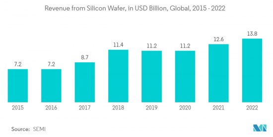
- The rise in the expansion of the wafer production plants will create an opportunity for the local and international wafer inspection players to develop new products according to the customer's requirements. For instance, according to SEMI, in 2022, the silicon wafer area shipments worldwide amounted to 14.71 billion square inches, which increased from 14.16 billion square inches in 2021. Silicon wafers are a vital building material for semiconductors, which indicates the usage of high-performance semiconductors in connected devices and driving the market. Further, in 2022, the total revenue from silicon wafers worldwide amounted to USD 13.8 billion, which increased from USD 12.6 billion, further indicating the market's growth.
Asia-Pacific to Dominate the Market
- The Asia-Pacific is one of the prominent regions for the semiconductor industry concerning manufacturing and consumption. According to SIA, Asia-Pacific is the largest regional semiconductor market, and China accounts for the most significant share in the region.
- Many regional companies are entering collaborations and partnerships in the semiconductor metrology/inspection equipment market. For instance, Shenzhen JT Automation Equipment, a chip production tool manufacturer in China, announced a legally binding five-year (2021-2025) memorandum of understanding with Huawei's HiSilicon Technologies business, China's largest chip developer. Both firms aim to extend their partnership for the development of semiconductor packaging tools, creating a self-sufficient and regulated industry.
- Asia-Pacific has been a growing market for semiconductor equipment over the last few years. For instance, according to SEMI, in 2022, China remained the leading spender on semiconductor equipment with USD 28.3 billion in billings. However, trade issues between the United States and China have presented uncertainty in the semiconductor metrology and inspection equipment market. Domestic semiconductor companies have been spending significantly to maintain their current market position by increasing their capacity and transitioning between technology nodes and wafer sizes. In the future, the demand is expected to be witnessed from the foundry in the region.
- The regional government's initiatives to develop the local semiconductor industry also creates a favorable outlook for the growth of the studied market. For instance, China's State Council's "National Integrated Circuit Industry Development Guidelines" aims to make the country a global leader in all the segments of the semiconductor industry by 2030. Additionally, the Made in China 2025 initiative maintains achieving knowledge concerning advanced semiconductor manufacturing as a vital component of China's future economy. It is highly focused on building the strategy for a strong manufacturing nationwide.
- The initiative is also expected to encourage local and foreign companies to invest in various segments of semiconductor manufacturing including integrated circuits. The initiative prompts the government bodies to boost research and development activities so that China can rely on its own companies for core technologies rather than overseas ones. This is set to propel innovation in the semiconductor manufacturing industry.
Semiconductor Metrology & Inspection Equipment Industry Overview
The semiconductor metrology and inspection equipment market comprises prominent players such as Applied Materials Inc., Nikon Metrology NV, and KLA Corporation. These firms have continuously expanded their operation scales by focusing on market expansions and acquisitions. Acquisition activities effectively set the ball rolling regarding the overall market's growth in the market studied. Large companies have also been expending significant resources on R&D operations to protect their market position and drive innovation in the studied market shortly. Overall, the degree of competition remains high, primarily driven by the strong presence of prominent players involved in the market studied.
- July 2023: Applied Materials Inc. introduced materials, technologies, and systems that help chipmakers integrate chiplets into advanced 2.5D and 3D packages using hybrid bonding and through-silicon vias (TSVs). The new solutions will extend the company's industry-leading breadth of technologies for heterogeneous integration (HI). The company is the largest supplier of technologies for HI with optimized chipmaking systems spanning etch, physical and chemical vapor deposition (PVD), electroplating, chemical mechanical polishing (CMP), annealing, and surface treatments.
- May 2023: KLA Corporation announced a strategic partnership with imec to develop the talent base and infrastructure to accelerate the advanced semiconductor applications for autonomous mobility, electrification and move the automotive industry forward. Through this partnership, both partners plan to bring relevant expertise to identify and manage programs for automotive industry, as well as talent development and recruitment.
Additional Benefits:
- The market estimate (ME) sheet in Excel format
- 3 months of analyst support
TABLE OF CONTENTS
1 INTRODUCTION
- 1.1 Study Assumptions and Market Definition
- 1.2 Scope of the Study
2 RESEARCH METHODOLOGY
3 EXECUTIVE SUMMARY
4 MARKET INSIGHTS
- 4.1 Market Overview
- 4.2 Industry Attractiveness - Porter's Five Forces Analysis
- 4.2.1 Bargaining Power of Suppliers
- 4.2.2 Bargaining Power of Buyers
- 4.2.3 Threat of New Entrants
- 4.2.4 Threat of Substitutes
- 4.2.5 Degree of Competition
- 4.3 An Assessment of the Impact of Key Macro Trends
5 MARKET DYNAMICS
- 5.1 Market Drivers
- 5.1.1 Increasing Demand for High-performance, Low-cost Semiconductors
- 5.1.2 Increasing Demand for Semiconductor Wafers in Consumer Electronics
- 5.2 Market Restraints
- 5.2.1 High Setup Cost and Lack of Expertise in Handling Metrology Systems Efficiently
- 5.2.2 High Raw Material and Fabrication Costs
6 MARKET SEGMENTATION
- 6.1 By Type
- 6.1.1 Lithography Metrology
- 6.1.1.1 Overlay
- 6.1.1.2 Dimension Equipment
- 6.1.1.3 Mask Inspection and Metrology
- 6.1.2 Wafer Inspection
- 6.1.3 Thin Film Metrology
- 6.1.4 Other Process Control Systems
- 6.1.1 Lithography Metrology
- 6.2 By Geography
- 6.2.1 North America
- 6.2.2 Europe
- 6.2.3 Asia-Pacific
- 6.2.4 Rest of the World
7 COMPETITIVE LANDSCAPE
- 7.1 Company Profiles
- 7.1.1 KLA Corporation
- 7.1.2 Applied Materials Inc.
- 7.1.3 Onto Innovation Inc.
- 7.1.4 Thermo Fisher Scientific Inc.
- 7.1.5 Hitachi Hi-Technologies Corporation (Hitachi Limited)
- 7.1.6 Nova Measuring Instruments Ltd
- 7.1.7 ASML Holding NV
- 7.1.8 Lasertec CorporatioN
- 7.1.9 JEOL Ltd
- 7.1.10 Nikon Metrology NV (Nikon Group)
- 7.1.11 Camtek Limited
8 INVESTMENT ANALYSIS
9 FUTURE OF THE MARKET
 2024 年半导体计量与检测全球市场报告
 半导体计量和检测市场报告:2030 年趋势、预测和竞争分析
 半导体测量·检验的全球市场 - 主要趋势与机会(~2029年)
 半导体计量设备市场 - 2023-2031 年全球行业分析、规模、份额、增长、趋势和预测
 不稳定(瞬态)分析软件全球市场规模研究和预测:按组件、部署模型、公司规模、最终用户、地区划分,2022-2029 年
 全球半导体计量和检测设备市场 - 按类型、组织规模和地区划分的市场规模、细分市场、前景和收入预测(2022-2028 年)
 半导体计量与检测市场:按类型、技术、组织规模分类:2021-2031 年全球机遇分析和行业预测
 半导体测量·检验的全球市场预测(到2028年):COVID-19影响,类型,技术,各组织规模的分析