


 |
市场调查报告书
商品编码
1432996
电子设计自动化 (EDA) 工具 -全球市场占有率分析、产业趋势、成长预测(2024-2029 年)Global Electronic Design Automation Tools (EDA) - Market Share Analysis, Industry Trends & Statistics, Growth Forecasts (2024 - 2029) |
||||||
※ 本网页内容可能与最新版本有所差异。详细情况请与我们联繫。
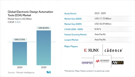
在预测期内(2024-2029),电子设计自动化(EDA)工具的全球市场规模预计到 2024 年为 177.2 亿美元,到 2029 年将达到 265.9 亿美元。预计将以复合年增长率增长8.46%。
市场扩张背后的主要因素是对小型电子设备的需求不断增长以及SoC技术在汽车、物联网和人工智慧等各个行业中的使用不断增加。
主要亮点
- 近年来,电子设计自动化(EDA)技术使硅领域取得了进展。 EDA 负责以生态系统有利可图的成本创建 IC 设计流程所需的设计工具。
- 使用 EDA 工具的好处包括减少复杂 IC 开发所需的时间、降低製造成本、消除製造缺陷、改进 IC 设计以及提高易用性。
- 根据世界半导体贸易统计(WSTS),预计2021年半导体产业将成长10.9%,达到约4,880亿美元,较前一年增速大幅成长。因此,预计各半导体供应商将增加研发预算。
- 晶片製造商越来越倾向于将人工智慧整合到边缘运算中。因为边缘运算在设备层级提供运算能力,从而提高效率和回应时间。例如,英特尔专注于“边缘运算”,实现人工智慧从物联网设备到智慧型手机的嵌入。
- EDA 因其许多优点而变得越来越普及,包括减少设计时间和减少错误。 EDA 工具已广泛应用于各种产业,包括汽车和航太产业。然而,EDA 的缺点之一是它不能提供对过去设计的洞察。
- 自半导体诞生以来,摩尔定律(积体电路中电晶体的数量将每 18 至 24 个月增加一倍的预测)一直被遵循。但近年来,科学家开始相信,基本的物理限制可能很快就会使在同一小区域经济地放置更多元素变得困难,并且摩尔定律可能被证明是错误的。
- 自COVID-19爆发以来,半导体产业受到严重影响,对供应链和生产设备造成重大影响。 2020 年 2 月和 3 月,中国大陆和台湾地区的生产暂停,影响了全球其他OEM生产。然而,很大一部分主要供应商在农历新年之前储备了电子设备,这降低了风险。此外,由于半导体产业成长放缓,疫情初期对 EDA 工具的需求略有下降,但这一市场在过去一年中有所增长。
EDA工具市场趋势
IC物理设计与检验领域显着成长
- IC 物理设计是指使用 EDA 工具建立 IC 的几何表示。 EDA用于将晶片划分为小块,并规划每个区块所需的特定空间,以确保最大性能。然后使用时钟合成前后放置这些块。
- 最近的技术进步鼓励晶片组製造商利用 ASIC 技术,主要用于 5G。结构化 ASIC 的出现,例如同时具有 ASIC 和现场可编程闸阵列 (FPGA) 元件的架构,导致了成熟的 ASIC 的出现,这导致了与 ASIC 相比更低的製造成本。
- 混合讯号晶片或具有类比和数位电路的积体电路 (IC) 是一种日益增长的趋势。混合讯号架构对于 SoC 和 ASIC 设计人员来说变得越来越重要。这种需求受到物联网、通讯、汽车工业、工业控制等产业的影响。例如,2022年7月,西门子EDA(原Mentor)混合讯号检验软体Symphony Pro获得重大更新。
- 同样在 2022 年 7 月,Siemens Digital Industries Software 宣布为积体电路 (IC) 实体检验的 Calibre 平台提供电子设计自动化 (EDA) 的各种增强型早期设计检验(EDV) 功能。这些新功能的开发旨在透过识别、分析和解决 IC 和系统晶片(SoC) 实体检验中的难题,帮助 IC 设计团队和公司更快地完成计划。将解决方案移至设计和检验的早期阶段流程中,我们帮助IC 设计人员「委託」实体和电路检验任务。
- 此外,2022年2月,国际知名电子设计服务供应商Veriest Solutions宣布将服务范围扩大到包括实体设计服务,并在英国建立了一个设计中心。英国的新专家团队将使该公司的现有客户和新客户能够获得可测试设计(DFT)和实体设计支援。新团队还将帮助电子系统公司将整个 ASIC 设计计划委託给 Veriest,满足客製化半导体设计高品质解决方案日益增长的需求。
预计北美将占据较大市场占有率
- EDA 工具通常用于设计电路基板、处理器和其他复杂的电子设备。随着EDA工具在家电和汽车等行业的采用,北美市场需求预计将增加。此外,半导体和电路製造业新兴市场的开拓正在增加 EDA 工具在该地区的存在。此外,一些主要 EDA 工具供应商的总部位于北美,包括 Xilinx、Ansys、Keysight Technologies、Cadence Design Systems 和 Synopsys。
- 一些北美供应商正在投资扩大其产品线和企业范围,以满足该地区对 EDA 工具的需求。例如,晶片製造商 Advanced Micro Devices 于 2022 年 5 月宣布,打算将部分用于晶片设计的电子设计自动化工作负载转移到 Google Cloud,以扩展其资料中心的功能。这使您可以利用 Google 最新的运算优化的 C2D虚拟机实例,该实例由第三代 AMD EPYC 处理器提供支持,并具有先进的网路、储存和人工智慧功能。
- 一些供应商继续看到客户的强劲需求,他们希望加快数位转型,以应对日益激烈的竞争和更快的上市时间。例如,英特尔代工服务 (IFS) 于 2022 年 7 月宣布了一项全新的云端联盟计划,作为其加速器计划的一部分。云端联盟透过按需运算提高代工客户的设计效率,同时保护云端中的设计环境。 Ansys、Cadence、Siemens EDA 和 Synopsys 以及电气设计自动化 (EDA) 领域的其他知名企业都是云端联盟的创始成员。
- 2021年6月,台积电(TSMC)将投资120亿美元在亚利桑那州建造电脑晶片工厂,并于2024年开始采用该公司5奈米製造技术大规模生产晶片,打算有所作为。此外,2021年4月,该公司宣布了一项1,000亿美元的投资计划,以在未来三年内增加工厂产能。
- 美国是半导体产业製造、设计和研究的重要国家。该地区的崛起正在推动电子产品的出口需求以及消费性电子产品和汽车行业等最终用户行业的成长,这些行业是半导体的重要消费者。例如,美国半导体公司半导体产业协会(SIA)2022年2月公布,2021年全球半导体产业收益达5,559亿美元,创历史最高年度总额,2020年总额为4,404亿美元。成长26.2%。由于晶片製造商增加产量以满足全球晶片短缺带来的强劲需求,2021年半导体产业出货达到1.15兆台的历史新高。
EDA工具产业概况
EDA 市场高度分散。汽车、物联网、人工智慧和虚拟/扩增实境领域的新商机使半导体公司能够在 IC 生产週期的各个阶段蓬勃发展,从而实现收入的显着增长。儘管晶片性能显着提高,但单位销售价格仍相对持平。该行业的一些主要企业包括 ANSYS、Cadence Design Systems、 摘要和 Keysight Technologies。 EDA 市场的主要发展包括:
- 2022 年 3 月 - Synopsys 宣布推出专为云端设计的新电子设计自动化 (EDA) 部署模式。该模型透过单一来源、付费使用制提供了「无与伦比的晶片和系统设计弹性」。借助 Microsoft Azure 上预先优化的基础设施,Synopsys Cloud 提供对云端优化设计和检验技术的访问,以解决晶片开发中日益增加的相互依赖性。
- 2021 年 6 月 - Xilinx 宣布推出 Vivado ML Editions,这是一款 FPGA EDA 工具包,可基于机器学习 (ML) 优化技术和基于团队的先进设计程序显着缩短设计时间和成本。将新的 Vivado ML 版本与现有的 Vivado HLx 版本进行比较,前者的编译时间加快了五倍,并且在具有挑战性的设计中实现了突破性的结果品质 (QoR) 平均提高 10%。
- 2021 年 6 月 - Aldec 开始提供 HES-DVM 原型云端版本 (CE)。 HES-DVM Proto CE 可用于对基于 FPGA 的 SoC/ASIC 设计原型製作,并专注于自动化设计分区,当需要多达四个 FPGA 来容纳一个推出时间。
- 2021 年 5 月 - Cadence Design Systems 宣布推出适用于 PCI Express 5.0 规范的低功耗 IP,针对采用台积电 N5 製程技术製造的超大规模运算、网路和储存应用。此外,PCIe 5.0技术由PHY、伴同性控制器和检验IP(VIP)组成,针对适合应用的超高频宽SoC设计。
其他福利:
- Excel 格式的市场预测 (ME) 表
- 3 个月分析师支持
目录
第一章简介
- 研究假设和市场定义
- 调查范围
第二章调查方法
第三章执行摘要
第四章市场洞察
- 市场概况
- 产业价值链分析
- 产业吸引力波特五力分析
- 供应商的议价能力
- 买方议价能力
- 新进入者的威胁
- 竞争公司之间敌对关係的强度
- 替代品的威胁
- 评估 COVID-19 对产业的影响
第五章市场动态
- 市场驱动因素
- 汽车、IoT、AI领域的活动
- 具有机器学习功能的 EDA 工具集的趋势
- 市场限制因素
- 摩尔定律的失败
第六章市场区隔
- 类型
- 电脑辅助工程(CAE)
- IC物理设计与检验
- 印刷基板和多晶片模组(PCB 和 MCM)
- 半导体智慧财产权(SIP)
- 服务
- 目的
- 通讯
- 消费性电子产品
- 车
- 产业
- 其他用途
- 地区
- 北美洲
- 欧洲
- 亚太地区
- 世界其他地区
第七章 竞争形势
- 公司简介
- Altium Limited
- Ansys Inc.
- Cadence Design Systems Inc.
- Keysight Technologies Inc.
- Agnisys Inc.
- Aldec Inc.
- Lauterbach GmbH
- Mentor Graphic Corporation(Siemens PLM Software)
- Synopsys Inc.
- Xilinx Inc.
- Zuken Ltd.
第八章投资分析
第9章市场的未来
The Global Electronic Design Automation Tools Market size is estimated at USD 17.72 billion in 2024, and is expected to reach USD 26.59 billion by 2029, growing at a CAGR of 8.46% during the forecast period (2024-2029).
The main factors propelling the market's expansion are the growing need for compact electronic devices and the expanding use of SoC technology across various industries, including automotive, IoT, and AI.
Key Highlights
- The silicon sector has evolved in recent years because of electronic design automation (EDA) techniques. EDA is responsible for creating the design tools necessary for the IC design process at a cost that enables the ecosystem to run profitably.
- Some of the benefits of using EDA tools include reducing the amount of time needed to develop complicated ICs, cutting manufacturing costs, eliminating manufacturing defects, improving IC design and ease of use, etc.
- According to World Semiconductor Trade Statistics (WSTS), the semiconductor industry is expected to grow by 10.9% in 2021, which is a significant growth compared to the previous year's growth, approximately amounting to USD 488 billion. Owing to this, various semiconductor vendors are expected to increase their R&D budgets. For instance, in April 2021, Taiwan Semiconductor Manufacturing Corporation ( TSMC) announced to spend USD 100 billion over the next three years to expand its chip fabrication capacity and R&D.
- Chipmakers are increasingly leaning toward incorporating AI on edge computing, owing to the computational capabilities it brings to the table at the device level, increasing both efficiency and response time. For instance, Intel is focusing on 'edge computing' to enable AI incorporation into IoT devices to smartphones.
- EDA has become more popular due to its many benefits, including shorter design times and fewer errors. EDA tools have become more widely used in various industries, including the automotive and aerospace industries. However, one of EDA's shortcomings lies in its inability to obtain insights from previous designs.
- Since the inception of semiconductors, Moore's Law-the prediction that the number of transistors in an integrated circuit will increase two-fold every 18-24 months-has held true. However, in recent years, scientists have increasingly come to believe that fundamental physical limits may soon make it hard to economically place additional elements on the same small area, which could ultimately prove that Moore's Law is faulty.
- Since the COVID-19 breakout, the semiconductor industry has been severely impacted, significantly impacting its supply chain and production facilities. In February and March 2020, China and Taiwan's production ceased, affecting other OEM production worldwide. However, a significant portion of important vendors stocked up on electronics in anticipation of the Chinese New Year, which reduced the risk. Additionally, with the semiconductor industry's slowing growth, the initial pandemic epidemic saw a minor decline in demand for EDA tools; but, over the course of a year, the market experienced growth.
EDA Tools Market Trends
IC Physical Design and Verification Segment to Grow Significantly
- IC physical design refers to the creation of geometric representations of ICs, using EDA tools. EDA is used to divide the chip into smaller blocks and then plan the specific space required for each block to ensure maximum performance. These blocks are then placed, using before and after clock synthesis.
- The recent technological advancements have been helping several chipset manufacturers to make use of ASIC technology, mainly for 5G. The advent of structured ASIC, having elements of both ASICs and field-programmable gate arrays (FPGA), like architecture, has led to the cost of production becoming cheaper compared to full-blown ASIC, which requires the addition of a modifiable on top of the base ASIC layer.
- Mixed-signal chips, or integrated circuits (ICs) featuring analog and digital circuitry, are a growing trend. Mixed-signal architectures are becoming progressively and more necessary for SoC and ASIC designers. This demand is influenced by industries including the internet of things, communications, the automobile industry, and industrial control. For instance, in July 2022, the mixed-signal verification software Symphony Pro had a significantly updated version from Siemens EDA (previously Mentor).
- Also, in July 2022, Siemens Digital Industries Software announced a variety of expanded early design verification (EDV) functions for electronic design automation (EDA) for its Calibre platform for integrated circuit (IC) physical verification. These new capabilities, which were developed to assist IC design teams and businesses in completing projects more quickly, can assist IC designers in "shifting left" their physical and circuit verification tasks by putting the identification, analysis, and resolution of challenging IC and system-on-chip (SoC) physical verification issues into earlier stages of the design and verification flow.
- Furthermore, in February 2022, Veriest Solutions, a prominent international provider of electronics design services, built a design center in the United Kingdom and announced the expansion of its offerings to include physical design services. Customers of the company, both current and new, will now have access to Design for Test (DFT) and Physical Design support due to the new specialist team in the United Kingdom. The inclusion of the new team will also allow electronic system firms to outsource whole ASIC design projects to Veriest, meeting the growing need for high-quality solutions for customized semiconductor designs.
North America is Expected to Hold a Significant Market Share
- EDA tools often design circuit boards, processors, and other complex electronics. The adoption of EDA tools in industries such as consumer electronics, and automotive, is set to increase demand for the market in North America. Also, growing developments in the semiconductor industry and circuit manufacturing industry have raised the market's prominence in the region. Also, some of the significant vendors of EDA tools are headquartered in North America, such as Xilinx Inc., Ansys Inc., Keysight Technologies Inc., Cadence Design Systems Inc., and Synopsys Inc.
- Some North American suppliers have been investing in improving the company's product lines and broadening the firm reach to meet the demand for EDA tools in the region. For instance, in May 2022, Chipmaker Advanced Micro Devices Inc. announced that the company intends to move some of its electronic design automation workloads for chip design onto Google Cloud to expand the capabilities of the company's data centers. This will allow taking advantage of Google's most recent compute-optimized C2D virtual machine instances, which are powered by 3rd Gen AMD EPYC processors, as well as advanced networking, storage, and artificial intelligence capabilities.
- Some of the vendors have continued to see strong demand from their customers, who are looking forward to accelerating their digital transformation as engineering teams adapt to increasing competition and shrinking time to market windows. For instance, in July 2022, Intel Foundry Services (IFS) unveiled a brand-new Cloud Alliance program as a component of its Accelerator program. Cloud Alliance streamlines design efficiency for foundry clients with on-demand computing while securing design environments on the cloud. Ansys, Cadence, Siemens EDA, and Synopsys are a few of the founding members of the Cloud Alliance, along with other prominent companies in electrical design automation (EDA).
- In June 2021, Taiwan-based Semiconductor Manufacturing Co. Ltd (TSMC) started construction at a site in Arizona where it plans to spend USD 12 billion to build a computer chip factory, which will begin volume production of chips using the company's 5-nanometer production technology starting in 2024. The company also announced a USD 100 billion investment plan in April 2021 to increase capacity at its factories over the next three years.
- The United States is a significant country in the semiconductor industry's manufacturing, design, and research. The region's prominence drives the demand for exporting electronics equipment and growing end-user industries that are significant consumers of semiconductors, such as consumer electronics and the automotive industry. For instance, the US semiconductor company, the Semiconductor Industry Association (SIA), in February 2022, reported that revenues for the worldwide semiconductor industry reached USD 555.9 billion in 2021, the highest yearly total ever and a rise of 26.2% over the USD 440.4 billion total for 2020. In 2021, the semiconductor industry shipped a record 1.15 trillion units as chip companies increased output to meet the strong demand brought on by the worldwide chip shortage.
EDA Tools Industry Overview
The EDA market is highly fragmented. New opportunities in the automotive, IoT, artificial intelligence and virtual/augmented reality sectors have allowed semiconductor companies throughout all phases of the IC production cycle to prosper, with sizable revenue increases. This has occurred despite significant gains in chip performance but at relatively flat unit sales prices. Some of the key players in the industry include ANSYS, Cadence Design Systems, Synopsis, Keysight Technologies, etc. Some of the key developments in the EDA market are as follows:
- March 2022 - Synopsys has announced the introduction of a new electronic design automation (EDA) deployment model that is designed for the cloud and provides "unparallel levels of chip and system design flexibility" through a single-source, pay-as-you-go approach. With pre-optimized infrastructure on Microsoft Azure, Synopsys Cloud provides access to the company's cloud-optimized design and verification technologies, which address increased levels of interdependencies in chip development.
- June 2021 - Xilinx, Inc. unveiled Vivado ML Editions, an FPGA EDA tool package based on machine learning (ML) optimization techniques and advanced team-based design procedures for considerable design time and cost savings. Comparing the new Vivado ML Editions to the existing Vivado HLx Editions, the former offers a 5x quicker compilation time and revolutionary quality of results (QoR) improvements that average 10% on difficult designs.
- June 2021 - Aldec Inc. launched HES-DVM Proto Cloud Edition (CE). It is available through Amazon Web Service (AWS); HES-DVM Proto CE can be used for FPGA-based prototyping of SoC / ASIC designs and focuses on automated design partitioning to greatly reduce bring-up time when up to four FPGAs are needed to accommodate a design.
- May 2021- Cadence Design Systems announced low-power IP for the PCI Express 5.0 specification that targets hyper-scale computing, networking, and storage applications that are made on TSMC N5 process technology. In addition, PCIe 5.0 technology consists of a PHY, companion controller, and Verification IP (VIP) targeted at SoC designs for very high bandwidth to suit the applications.
Additional Benefits:
- The market estimate (ME) sheet in Excel format
- 3 months of analyst support
TABLE OF CONTENTS
1 INTRODUCTION
- 1.1 Study Assumptions and Market Definition
- 1.2 Scope of the Study
2 RESEARCH METHODOLOGY
3 EXECUTIVE SUMMARY
4 MARKET INSIGHTS
- 4.1 Market Overview
- 4.2 Industry Value Chain Analysis
- 4.3 Industry Attractiveness: Porter's Five Forces Analysis
- 4.3.1 Bargaining Power of Suppliers
- 4.3.2 Bargaining Power of Buyers
- 4.3.3 Threat of New Entrants
- 4.3.4 Intensity of Competitive Rivalry
- 4.3.5 Threat of Substitute Products
- 4.4 Assessment of the Impact of COVID-19 on the Industry
5 MARKET DYNAMICS
- 5.1 Market Drivers
- 5.1.1 Booming Automotive, IoT, and AI Sectors
- 5.1.2 Upcoming Trend of EDA Toolsets Equipped with Machine Learning Capabilities
- 5.2 Market Restraints
- 5.2.1 Moore's Law about to be Proven Faulty
6 MARKET SEGMENTATION
- 6.1 Type
- 6.1.1 Computer-aided Engineering (CAE)
- 6.1.2 IC Physical Design and Verification
- 6.1.3 Printed Circuit Board and Multi-chip Module (PCB and MCM)
- 6.1.4 Semiconductor Intellectual Property (SIP)
- 6.1.5 Services
- 6.2 Application
- 6.2.1 Communication
- 6.2.2 Consumer Electronics
- 6.2.3 Automotive
- 6.2.4 Industrial
- 6.2.5 Other Applications
- 6.3 Geography
- 6.3.1 North America
- 6.3.2 Europe
- 6.3.3 Asia Pacific
- 6.3.4 Rest of the World
7 COMPETITIVE LANDSCAPE
- 7.1 Company Profiles
- 7.1.1 Altium Limited
- 7.1.2 Ansys Inc.
- 7.1.3 Cadence Design Systems Inc.
- 7.1.4 Keysight Technologies Inc.
- 7.1.5 Agnisys Inc.
- 7.1.6 Aldec Inc.
- 7.1.7 Lauterbach GmbH
- 7.1.8 Mentor Graphic Corporation (Siemens PLM Software)
- 7.1.9 Synopsys Inc.
- 7.1.10 Xilinx Inc.
- 7.1.11 Zuken Ltd.
8 INVESTMENT ANALYSIS
9 FUTURE OF THE MARKET
 云端 EDA 市场:按类型、应用程式划分 - 2025-2030 年全球预测
 电子设计自动化软体市场:按类型、应用分类 - 2025-2030 年全球预测
 全球电子设计自动化 (EDA) 市场
 电子设计自动化软体市场报告:2030 年趋势、预测与竞争分析
 电子设计自动化 (EDA) 市场:产业分析、规模、占有率、成长、趋势、预测 (2024-2033)
 亚太地区光子设计自动化市场预测至 2030 年 - 区域分析 - 按组件、部署、组织规模和应用
 北美光子设计自动化市场预测至 2030 年 - 区域分析 - 按组件、部署、组织规模和应用
 欧洲光子设计自动化市场预测至 2030 年 - 区域分析 - 按组件、部署、组织规模和应用
 全球电子设计自动化 (EDA) 市场 2024-2028
 云端电子设计自动化市场 - 全球产业规模、份额、趋势、机会和预测,按类型、应用、地区、竞争细分,2019-2029F