


 |
市场调查报告书
商品编码
1687460
半导体 CVD 设备:市场占有率分析、产业趋势与统计、成长预测(2025-2030 年)Semiconductor CVD Equipment - Market Share Analysis, Industry Trends & Statistics, Growth Forecasts (2025 - 2030) |
||||||
※ 本网页内容可能与最新版本有所差异。详细情况请与我们联繫。
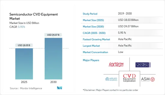
半导体 CVD 设备市场规模预计在 2025 年为 180.3 亿美元,预计到 2030 年将达到 240.7 亿美元,预测期内(2025-2030 年)的复合年增长率为 5.95%。
对基于微电子的消费产品的需求不断增长,推动了半导体、LED 和储存设备行业的蓬勃发展,而对 Cr6 电镀使用的严格规定主要推动了 CVD 设备市场的成长。
主要亮点
- 化学气相沉积(CVD)製程常用于半导体製造和薄膜生产。近年来,CVD合成技术已达到新的高度,能够精密製造二维材料的无机薄膜以及可在多种基板上保形沉淀的高纯度聚合物薄膜。
- 在半导体化学气相沉积系统中,前驱气体(通常在载气中稀释)被输送到接近常温的反应室。当这些气体通过或接触到加热的基板时,它们会发生反应或分解,产生沉积在基板上的固相。基板的温度很重要,因为它会影响发生的反应。
- CVD 是一种广泛使用的微加工技术,用于沉积各种形态的材料,包括多晶、结晶、非晶质和外延。这些材料包括硅(氧化物、碳化物、氮化物、氧氮化物)、碳(纤维、奈米纤维、奈米管、钻石、石墨烯)、氟碳化合物、细丝、钨、氮化钛和各种高 k 电介质。
- 新兴国家的政府和相关人员正在密切关注微电子产业的发展,因为这些技术有可能颠覆和推动物联网市场的发展。随着虚拟和扩增实境设备的普及,微电子研究和开发也可能增加,以应对迫在眉睫的频宽限制。
- 他们製造半导体。 CVD 设定复杂且成本高。随着代工厂和半导体组装和测试公司(OSAT)不断扩大产量以满足不断增长的晶片需求,资本支出压力可能会增加。
- 新冠疫情对整个半导体和晶片製造市场的需求和供应都产生了影响。全国各地半导体工厂的停工关闭,进一步加剧了供不应求趋势。然而,这些影响可能是短暂的,只会对 CVD 技术的需求产生暂时影响。此外,世界各国政府为支持汽车和工业领域所采取的预防措施可能有助于恢復铸造业的成长。
半导体 CVD 市场趋势
微电子和消费性电子产品需求不断增长将推动需求
- 预计预测期内微电子和消费性电子产品销售的成长将推动半导体积体电路的需求。然而,对半导体积体电路的需求预计将提高半导体装置製造商的生产能力,从而可能增加对化学气相沉积市场的需求。
- 集成设备製造商 (IDM) 包括逻辑、光电子、感测器、分立元件等。 (除「记忆製造者」外)。集成设备製造商製造和销售积体电路(IC)。典型的 IDM 拥有自有品牌,自行设计并在自己的工厂生产。当IDM追求节点从10nm缩小到5nm再到3nm时,其他製造商正在放弃平面架构,转而采用复杂的3D(3D)逻辑和记忆体结构。
- 薄膜沉积是积体电路(IC)製造的关键步骤。最常见的薄膜生长方法是 CVD。在 CVD 中,前体和反应物在处理室中混合,然后以稳定状态输送以在晶圆上形成薄膜。
- 在竞争激烈的市场中,各种IDMS采取不同的方法来取得竞争优势。例如,加拿大光子製造中心(CPFC)是一家提供製造服务、预商用光子设备和光子积体电路製造商的机构。设计和建模、外延、製造、测试和功能描述是 CPFC 提供的付费服务之一。 CPFC 运作金属有机化学气相沉积 (MOCVD) 反应器,用于研究和製造基于砷化镓 (GaAs) 和磷化铟 (InP) 的设备。
- 此外,政府和相关人员正在密切关注微电子产业的进步,因为这些技术有可能颠覆和激发物联网市场。由于虚拟和扩增实境(AR)设备的日益普及以及迫在眉睫的频宽紧缩,微电子研究和开发也可能增加。 2021年9月,德国政府主办了一场来自欧洲和国际半导体产业的50名代表的会议,透过提出支持措施来说服他们在德国投资。德国政府计划斥资约 45 亿美元重新夺回半导体价值链的製造地。
亚太地区是全球半导体CVD设备利润最丰厚的市场
- 亚太地区是一个潜力巨大的地区,拥有开发消费性电子产品和半导体相关产品的各种製造设施。预计未来几年该地区将占据半导体 CVD 设备市场最大的市场占有率。
- 尤其是中国电子和半导体产业的发展正在推动该地区的市场扩张。在中国和印度等发展中经济体中,工业化程度的提高以及终端用户行业和企业数量的增加带来了巨大的未开发潜力。由于新兴经济体的存在和电子产业的发展,预计该地区在预测期内将以显着的速度发展。
- 中国有非常雄心勃勃的半导体计划。在 1500 亿美元基金的支持下,中国计划发展国内积体电路产业并生产更多的晶片。大中华区包括中国香港和台湾,是一个地缘政治热点。美国贸易战进一步加剧了该地区的紧张局势,该地区是关键工艺技术的所在地,迫使许多中国公司投资半导体代工厂。
- 预计亚太地区汽车半导体产业的快速扩张将受到电动车不断增长的需求的推动。虽然汽车製造商必须继续创新、创造和开发自动驾驶汽车,但它们已经吸引了主要汽车製造国的众多客户。
- 印度由于人口众多,已成为世界上成长最快的经济体之一。据预测,未来几年该国汽车半导体市场将快速扩张。汽车产业拥有强大的半导体研发基础设施,这可能会在未来几年为印度半导体蚀刻市场开闢新的可能性。
半导体 CVD 产业概况
市场分散,竞争对手激烈。此外,由于竞争对手的市场渗透率和提供先进产品的能力,预计他们之间的敌意也会很强烈。市场由各种参与者组成,但只有少数参与者凭藉高标准和卓越品质脱颖而出。
其他福利:
- Excel 格式的市场预测 (ME) 表
- 3 个月的分析师支持
目录
第 1 章 简介
- 研究假设和市场定义
- 研究范围
第二章调查方法
- 研究框架
- 二次调查
- 初步调查
- 资料三角测量与洞察生成
第三章执行摘要
第四章 市场洞察
- 市场概况
- 产业吸引力-波特五力分析
- 供应商的议价能力
- 买家的议价能力
- 新进入者的威胁
- 替代品的威胁
- 竞争对手之间的竞争
- 价值链分析
- COVID-19 市场影响评估
第五章 市场动态
- 市场驱动因素
- 对微电子和半导体设备的需求不断增加
- 不断增加技术对多个最终用户的应用
- 市场限制
- 技术投入高
- CVD 製程技术概览
- 大气压力化学气相沉积 (APCVD)
- 高密度等离子化学气相沉积(DPCVD)
- 低压化学气相沉积 (LPCVD)
- 金属有机化学气相沉积 (MOCVD)
第六章 市场细分
- 按应用
- 铸件生产商
- 集成设备製造商 (IDM)
- 记忆製造者
- 按地区
- 北美洲
- 欧洲
- 亚太地区
- 世界其他地区
第七章 竞争格局
- 公司简介
- Aixtron Se
- Applied Materials, Inc.
- Asm International
- Cvd Equipment Corporation
- Oxford Instruments Plc
- Lam Research Corporation
- Tokyo Electron Limited
- Ulvac Inc.
- Veeco Instruments Inc.
第八章 市场投资
第九章 市场机会与未来趋势
The Semiconductor CVD Equipment Market size is estimated at USD 18.03 billion in 2025, and is expected to reach USD 24.07 billion by 2030, at a CAGR of 5.95% during the forecast period (2025-2030).
Increasing demand for microelectronics-based consumer products, resulting in the faster growth of the semiconductor, LED, and storage device industry and strict regulations on the use of Cr6 for electroplating are primarily driving the growth of the CVD equipment market.
Key Highlights
- The Chemical Vapor Deposition (CVD) process is often used in manufacturing semiconductors and producing thin films. In recent years, CVD synthesis has reached new heights with the precise manufacturing of both inorganic thin films of 2D materials and high-purity polymeric thin films that may be conformally deposited on various substrates.
- Precursor gases (typically diluted in carrier gases) are supplied into the reaction chamber at around ambient temperatures in semiconductor chemical vapor deposition equipment. They react or break down when they pass across or come into touch with a heated substrate, generating a solid phase that is deposited on the substrate. The temperature of the substrate is important because it can influence the reactions that occur.
- CVD is widely used in microfabrication techniques to deposit materials in various morphologies, including polycrystalline, monocrystalline, amorphous, and epitaxial. Silicon (dioxide, carbide, nitride, oxynitride), carbon (fiber, nanofibers, nanotubes, diamond, and graphene), fluorocarbons, filaments, tungsten, titanium nitride, and a variety of high-k dielectrics are among these materials.
- Governments and business stakeholders are watching developments in the microelectronics industry closely because these technologies have the potential to disrupt and propel the Internet of Things market. Due to the increased adoption of virtual reality and augmented reality gadgets, R&D for microelectronics may also increase in response to the looming bandwidth constraint.
- They are making semiconductors. CVD setup can be complex and comes with huge costs. The foundries and Outsources Semiconductor Assembly and Test (OSAT) companies are likely to face increased pressure on capital expenditures as they continue to expand production to address the rising chip demand.
- The COVID -19 outbreak affected the overall semiconductor and chip fabrication market from the demand and supply sides. The nationwide lockdowns and closure of semiconductor plants have further fueled the supply shortage trend. However, these effects are likely to be short-term and temporarily affect the demand for CVD technologies. Moreover, government precautions globally to support automotive and industrial sectors could help revive foundry industry growth.
Semiconductor CVD Market Trends
Increase in Demand for Microelectronics and Consumer Electronics to Fuel the Demand
- The rise in microelectronics and consumer electronics sales is expected to drive the demand for semiconductor ICs over the forecasted period. However, the demand for semiconductor ICs is expected to increase the production capacity of semiconductor device manufacturers, which may augment the demand in the chemical vapor deposition market.
- The integrated device manufacturer (IDM) includes logic, optoelectronics, sensors, discrete components, and others. (Excluding Memory Manufacturers). An integrated device manufacturer manufactures and sells integrated circuits (ICs). A classic IDM owns its branded chips, designs them in-house, and makes them in a fabrication factory. IDMs pursue node scaling beyond 10 nm to 5 nm and even 3 nm, while other manufacturers renounce planar architectures favoring sophisticated, three-dimensional (3D) structures for logic and memory.
- Thin-film deposition is a vital step in manufacturing integrated circuits (ICs). The most common approach for thin-film growth is CVD. Precursors and reactants are combined in a process chamber before being delivered in a steady state to form a film on the wafer in CVD.
- The market is witnessing the presence of various IDMS undertaking different initiatives to gain a competitive advantage. For instance, the Canadian Photonics Fabrication Centre (CPFC) is a facility that provides fabrication services, pre-commercial photonic devices, and photonic integrated circuit manufacturers. Design and modeling, epitaxy, fabrication, and test and characterization are among the fee-based services provided by CPFC. CPFC operates a metal-organic chemical vapor deposition (MOCVD) reactor for the research and fabrication of gallium arsenide (GaAs) and indium phosphide (InP)-based devices.
- Also, governments and industry stakeholders are keenly following the advances in the microelectronics industry as these technologies might potentially disrupt and boost the Internet of Things market. R&D for microelectronics may also increase with the impending bandwidth crunch due to the improved penetration of virtual reality and augmented reality devices. In September 2021, the government organized a conference with 50 European and international semiconductor industry representatives to persuade them to invest in Germany by offering them a help package. The German government plans to spend roughly USD 4.5 billion to recapture manufacturing locations across the semiconductor value chain.
Asia Pacific as the Most Lucrative Market for Global Semiconductor CVD Equipment
- The Asia Pacific is a potential region with various manufacturing facilities for developing consumer electronics and semiconductor-related products. The particular region is expected to occupy the largest market share in the semiconductor CVD equipment market in the coming years.
- The advancement of the electronics and semiconductor industries, particularly in China, is driving market expansion in the region. In growing economies like China and India, the expansion in industrialization and the number of end-user sectors and companies presented enormous undiscovered potential. Due to the sheer existence of growing economies and the development of the electronics industries, the region is predicted to propel at a significant rate over the forecast period.
- China has a very ambitious semiconductor agenda. Backed by USD 150 billion in funding, the country is developing its domestic IC industry and plans to make more of its chips. Greater China, which encompasses Hong Kong, China, and Taiwan, is a geopolitical hotspot. The US-China trade war is compounding tensions in an area where all the leading process technology is located, forcing many Chinese companies to invest in their semiconductor foundries.
- The rapid expansion of the APAC automotive semiconductor industry is expected to be fueled by the rising demand for electric vehicles. Automobile manufacturers must continue to innovate, create, and develop self-driving cars, which have already attracted many customers in key automotive manufacturing countries.
- India has emerged as one of the world's fastest-growing economies due to its large population. According to projections, the automotive semiconductor market in the country will increase rapidly in the coming years. The Automotive industry is complemented by a strong semiconductor R&D infrastructure, which will open new potential for the semiconductor etch market in India in the forthcoming years.
Semiconductor CVD Industry Overview
The market is fragmented with high competitive rivalry. Also, owing to their market penetration and the ability to offer advanced products, the competitive rivalry is expected to be high. Although the market comprises various players, only a handful are prominent in the market for their high standards and excellent quality.
- August 2021 - CVD Equipment Corporation, one of the key suppliers of chemical vapor deposition systems, announced that it had secured a production system order worth about USD 1.7 million from a large US-based electric car battery material producer. In the first quarter of 2022, the system will be delivered to the customer.
- July 2021 - ASM International N.V. announced the availability of Intrepid ESATM epitaxy equipment for 300mm applications in power and analog devices and epitaxial silicon wafers. The new ESA tool increases ASM's atmospheric epi capabilities with ASM's first 300mm atmospheric cluster tool based on the proven, high-volume manufacturing Intrepid platform. On-wafer performance with the Intrepid ESA.
Additional Benefits:
- The market estimate (ME) sheet in Excel format
- 3 months of analyst support
TABLE OF CONTENTS
1 INTRODUCTION
- 1.1 Study Assumptions and Market Definition
- 1.2 Scope of the Study
2 RESEARCH METHODOLOGY
- 2.1 Research Framework
- 2.2 Secondary Research
- 2.3 Primary Research
- 2.4 Data Triangulation and Insight Generation
3 EXECUTIVE SUMMARY
4 MARKET INSIGHT
- 4.1 Market Overview
- 4.2 Industry Attractiveness - Porter's Five Forces Analysis
- 4.2.1 Bargaining Power of Suppliers
- 4.2.2 Bargaining Power of Buyers
- 4.2.3 Threat of New Entrants
- 4.2.4 Threat of Substitutes
- 4.2.5 Intensity of Competitive Rivalry
- 4.3 Value Chain Analysis
- 4.4 Assessment of Impact of Covid-19 on the Market
5 MARKET DYNAMICS
- 5.1 Market Drivers
- 5.1.1 Increase In Demand For Microelectronics And Semiconductor Devices
- 5.1.2 Rise In Application Of The Technology For Several End-users
- 5.2 Market Restraint
- 5.2.1 High Investment For The Technology
- 5.3 Cvd Processes Technology Snapshot
- 5.3.1 Atmospheric-pressure Chemical Vapor Deposition (apcvd)
- 5.3.2 Density-plasma Chemical Vapor Deposition (dpcvd)
- 5.3.3 Low-pressure Chemical Vapor Deposition (lpcvd)
- 5.3.4 Metal-organic Chemical Vapor Phase Deposition (mocvd)
6 MARKET SEGMENTATION
- 6.1 By Application
- 6.1.1 Foundry
- 6.1.2 Integrated Device Manufacturer (idm)
- 6.1.3 Memory Manufacturers
- 6.2 By Geography
- 6.2.1 North America
- 6.2.2 Europe
- 6.2.3 Asia-Pacific
- 6.2.4 Rest of The World
7 COMPETITIVE LANDSCAPE
- 7.1 Company Profiles
- 7.1.1 Aixtron Se
- 7.1.2 Applied Materials, Inc.
- 7.1.3 Asm International
- 7.1.4 Cvd Equipment Corporation
- 7.1.5 Oxford Instruments Plc
- 7.1.6 Lam Research Corporation
- 7.1.7 Tokyo Electron Limited
- 7.1.8 Ulvac Inc.
- 7.1.9 Veeco Instruments Inc.
8 MARKET INVESTMENTS
9 MARKET OPPORTUNITIES AND FUTURE TRENDS
 全球异质结PECVD设备市场
 2032 年化学沉淀沉积市场预测:按类型、沉淀材料、应用、最终用户和地区进行的全球分析
 2025 年化学气相沉积 (CVD) 全球市场报告
 2025-2033 年化学气相沉积设备市场报告(按技术(等离子体增强 CVD、低压 CVD、金属有机 CVD、常压 CVD 等)、应用、最终用户和地区)
 全球化学气相沉积市场(依类别、应用、地区):趋势分析、竞争格局、未来预测(2019-2031)
 全球半导体CVD(化学气相沉积)设备市场(2025-2029)
 化学气相成长市场:按产品、类型、形式、等级和最终用户划分 - 2025-2030 年全球预测
 化学气相沉积 (CVD) 市场 – 2025 年至 2030 年预测半导体化学气相沉积 (CVD) 设备市场规模、份额和趋势分析报告:按产品类型、应用、地区和细分市场预测,2024-2030 年
 化学气相沉积市场、占有率、规模、趋势、产业分析报告:依类别、依最终用途、依技术、依地区、依细分市场、预测,2024-2032年