


 |
市场调查报告书
商品编码
1693685
半导体键合设备:市场占有率分析、产业趋势与统计、成长预测(2025-2030)Semiconductor Bonding Equipment - Market Share Analysis, Industry Trends & Statistics, Growth Forecasts (2025 - 2030) |
||||||
※ 本网页内容可能与最新版本有所差异。详细情况请与我们联繫。
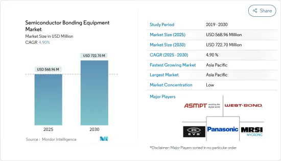
预计 2025 年半导体键合设备市场规模为 5.6896 亿美元,到 2030 年将达到 7.227 亿美元,预测期内(2025-2030 年)的复合年增长率为 4.9%。
由于对具有更高效率、处理能力和更小占地面积的半导体晶片的需求不断增加,半导体键合设备正在寻找应用,从而推动预测期内的市场需求。
关键亮点
- 随着数位化影响力的不断扩大,半导体市场正在蓬勃发展。值得注意的是,这促使政府推出进一步计画来支持 5G 的推出。例如,欧盟委员会很早就认识到5G网路的重要性,并建立了官民合作关係关係,共同开发和研究5G技术。
- 随着未来十年晶片需求的飙升,预计到 2030 年全球半导体产业将成为一个价值 1 兆美元的产业。推动这一成长的是企业和国家向半导体製造、材料和研究投入大量资金,确保晶片和技术的稳定供应,从而支撑日益以数据为中心的各行各业的成长。
- 生产关键技术部件的半导体行业由于需求激增而成为头条新闻。根据《华尔街日誌》近日报道,半导体是全球第四大交易商品(进出口总合),仅次于原油、精製油和汽车。这是因为半导体对于各种行业的高运算应用至关重要,包括电子、製造、农业、医疗保健、基础设施、娱乐、交通、通讯、军事系统、能源管理和太空。
- 当产品需要连接两个晶粒或晶圆时,会使用几种方法。除了选择键合方法本身的类型之外,您还必须决定键合的是晶圆还是晶粒。所选的接合製程是黏合拥有成本的主要因素。对于一个製程来说最重要的三个因素是键结所需的上游製程的成本、接合製程的週期时间和接合製程的产量比率。
- 全球疫情的爆发和为遏制COVID-19蔓延而采取的限制措施严重扰乱了半导体键合设备产业的全球供应链,影响了生产能力。儘管 COVID-19 感染人数已大幅下降,但仍需解决这些零件的材料供需方面的重大问题,这仍然是市场成长面临的挑战。
半导体键合设备市场趋势
电源IC和功率分离式元件元件应用领域占据较大的市场占有率
- 功率半导体装置有助于在各种应用中实现高效的电源管理、转换和控制。人们对节能和电力消耗的兴趣日益浓厚,功率半导体装置的重要性也日益凸显。该市场的驱动力在于减少损失、提高可控性、增强耐用性以及在正常和故障条件下的可靠性能。随着功率半导体需求的不断增加,功率IC和键结技术的市场也预计将扩大。
- 行业的快速数位化和互联设备的兴起正在推动这一领域的成长。这些设备需要高效的电源管理和高效能的功率半导体装置。利用这些设备可以实现最佳功率转换,减少能量损失,并提高电子系统的整体能源效率。
- 由于对节能和省电设备的需求不断增加,这一领域正在成长。无线和可携式电子产品的广泛应用、汽车行业向电气化的转变以及这些设备的使用日益增多进一步推动了这一需求。
- 各行各业越来越倾向于电源模组和整合解决方案。功率半导体製造商正在开发紧凑、高度整合的模组,整合开关、二极体和驱动器等各种功率元件,以简化系统设计、减少元件数量并提高整体系统效率。为了保持竞争力,功率半导体公司可以从在产品设计过程的早期了解障碍和市场趋势中受益。预计供应商增加投资以提高功率半导体产量将影响市场扩张。
- 电源 IC 和分立元件的重大发展使得电源管理更有效率。系统结构的最新进展减少了 AC-DC 电源供应器的尺寸和组件数量,从而提高了其效率。新的乙太网路供电 (PoE) 标准的推出实现了更高的电力传输能力,刺激了连网照明等创新设备类别的诞生。电子设备製造商越来越注重降低电力消耗,家用电子电器的需求不断增长,这是推动电源 IC 需求的主要因素。这些因素可能会刺激对黏合设备的需求。
- 智慧型手机的传输速度大幅提升,要求电池模组也能满足处理要求。电源转接器现在配备了离散半导体,由于电池供电设备的销售量增加,预计需求将激增。物联网应用的成长预计将进一步推动对离散半导体的需求。
- 例如,根据爱立信预测,全球蜂巢式物联网连线数将在 2022 年达到 19 亿,到 2027 年将达到 55 亿。由于 5G 的发展,智慧型手机的日益普及预计将推动市场成长。
- 同样,旨在为全球消费者提供技术增强和互联设备的物联网应用的重大技术进步也有望对市场成长产生积极影响。物联网应用的扩展正在推动智慧型设备和小型半导体的普及,从而导致对先进半导体键合设备的需求增加。
- 爱立信表示,2022 年至 2028 年间,全球连网装置的数量将约翻一番,这主要得益于短距离物联网设备的兴起。预计到2028年此类设备将达到约287.2亿台。随着物联网连接设备需求的扩大,预计电源IC的需求也将增加,从而推动键合设备市场的成长。
亚太地区可望成为成长最快的市场
- 半导体产业已成为亚洲经济成长的主要驱动力。它的快速扩张和技术进步使其成为全球供应链的重要组成部分。
- 亚太地区占据全球半导体代工厂的大部分份额,是三星电子、台积电等知名公司的所在地。韩国、台湾、日本和中国在该地区占有很大的份额。台湾拥有全球最大的晶圆代工市场份额之一,是半导体价值链中的重要地区。预计增加对该地区半导体製造能力的投资将极大促进市场成长。
- 2023年9月,中国推出一项400亿美元的基金,以促进其半导体产业的发展。中国正计划设立一个国家支持的投资基金,以帮助缩小与全球竞争对手(特别是美国)的差距。该基金可望发展成为中国积体电路产业投资基金(俗称大基金)管理的三支基金中最重要的一支。中国国家主席习近平强调实现半导体自给自足的重要性,这主要是为了回应美国的出口管制措施。该基金已获得中国相关部门核准,财政部将出资 600 亿元人民币(83 亿美元)。
- 基于国内晶片需求的成长,中国预计将超越美国成为全球最大的半导体产业强国。根据半导体产业协会预测,到2030年,半导体市场规模预计将扩大一倍,超过1兆美元,其中中国将占成长的60%以上。预计这种快速增长将增加对半导体键合设备的需求。
- 新的半导体晶圆厂将生产显示器驱动器、电源管理IC、微控制器和高效能运算逻辑等应用的晶片,以满足运算、资料储存、汽车、无线通讯和人工智慧等市场日益增长的需求。该晶圆厂的月产能为 50,000 片晶圆,预计将于 2026 年底出货首批晶片。
半导体键结设备市场概况
半导体键合设备市场高度分散,主要参与者包括 EV Group、ASMPT Semiconductor Solutions、MRSI Systems(Myronic AB)、WestBond Inc. 和松下控股公司。市场参与企业正在参与联盟和收购以获得可持续的竞争优势并加强其产品组合。
- 2023 年 11 月 - EV 集团 (EVG) 宣布 EVG 总部扩建下一阶段工程完工。 「製造 V」工厂将作为 EVG 的设备零件製造部门,并将显着扩大其生产车间和仓库空间。 Manufacturing V 工厂的开幕标誌着 EVG 最新的扩张倡议和投资。 EVG 继续受益于对其混合键合解决方案和其他製程解决方案及製程开发服务的持续高需求,以支援快速成长的先进封装和 3D/异质整合市场。
- 2023 年 9 月 - MRSI Systems(Mycronic AB)宣布推出成熟的 MRSI-7001 平台的新版本:MRSI 7001HF。 7001HF 具有加热键合头,键合时能够施加高达 500N 的力。此加热键合头也可从顶部加热,温度最高可达 400°C。这使得 7001HF 成为 IC 封装功率半导体烧结和 IC 封装热压键合机等应用的高负载晶片键合机的完美工具。
其他福利
- Excel 格式的市场预测 (ME) 表
- 3个月的分析师支持
目录
第一章 引言
- 研究假设和市场定义
- 研究范围
第二章调查方法
第三章执行摘要
第四章 市场洞察
- 市场概览
- 市场吸引力—波特五力分析
- 供应商的议价能力
- 买家的议价能力
- 新进入者的威胁
- 替代品的威胁
- 竞争对手之间的竞争
- 产业价值链/供应链分析
- COVID-19 市场影响
第五章市场动态
- 市场驱动因素
- 半导体製造商正在加大投资以扩大其製造能力
- 各种应用对半导体晶片的需求不断增加
- 市场限制
- 拥有成本高
- 电路小型化带来的复杂性
第六章市场区隔
- 按类型
- 永久黏合设备
- 临时黏合设备
- 混合键合设备
- 按应用
- 先进封装
- 电源IC和功率分离式元件
- 光子装置
- MEMS感测器和致动器
- 工程师基板
- 射频设备
- CMOS影像感测器(CIS)
- 按地区
- 北美洲
- 欧洲
- 亚洲
- 澳洲和纽西兰
- 拉丁美洲
- 中东和非洲
第七章竞争格局
- 公司简介
- EV Group
- ASMPT Semiconductor Solutions
- MRSI Systems.(Myronic AB)
- WestBond Inc.
- Panasonic Holding Corporation
- Palomar Technologies
- Dr. Tresky AG
- BE Semiconductor Industries NV
- Fasford Technology Co.Ltd(Fuji Group)
- Kulicke and Soffa Industries Inc.
- DIAS Automation(HK)Ltd
- Shibaura Mechatronics Corporation
- SUSS MicroTec SE
- Tokyo Electron Limited
第八章投资分析
第九章:市场的未来
The Semiconductor Bonding Equipment Market size is estimated at USD 568.96 million in 2025, and is expected to reach USD 722.70 million by 2030, at a CAGR of 4.9% during the forecast period (2025-2030).
Semiconductor bonding equipment finds application owing to the rising demand for semiconductor chips with higher efficiency, processing power, and smaller footprint, thereby driving the demand for the market during the forecast period.
Key Highlights
- As the impact of digitalization has increased, semiconductor markets have boomed. Notably, this has further resulted in government programs to support the 5G deployment. For instance, the European Commission recognized the importance of the 5G network early and established a public-private partnership to develop and research 5G technology.
- With chip demand set to surge over the coming decade, the global semiconductor industry is expected to become a trillion-dollar industry by 2030. This growth is favored by companies and countries funneling vast sums of money into semiconductor manufacturing, materials, and research to guarantee a constant supply of chips and know-how to support growth across a broad swath of increasingly data-centric industries.
- The semiconductor industry, which makes crucial technological components, has been hitting the headlines due to a rampant demand increase. A recent Wall Street Journal report shows that semiconductors rank as the world's fourth-largest traded product (imports and exports, counted), after crude oil, refined oil, and cars. This is because semiconductors are critical for high-computing applications in various industries, including electronics and manufacturing industries, agriculture, healthcare, infrastructure, entertainment, transportation, telecommunications, military systems, energy management, and space, to name just a few.
- Several methods might be used when a product needs the bonding of two dies or wafers. Not only does the type of bonding method itself have to be selected, but it must also be decided whether the items being bonded will be in wafer or die form. The selected bonding process is the primary driver for the cost of ownership of bonding. For a given process, the three most important factors are the cost of the upstream process needed for bonding, the cycle time of the bonding process, and the yield of the bonding process.
- With the global outbreak of the pandemic and restrictive measures taken to control the spread of COVID-19, the global supply chain of the semiconductor bonding equipment industry was significantly disrupted, impacting the production capabilities of various companies. Although the number of COVID-19-infected patients decreased considerably, salient issues with materials supply and demand for these components still need to be addressed, challenging the market's growth.
Semiconductor Bonding Equipment Market Trends
Power IC and Power Discrete Application Segment Holds Significant Market Share
- Power semiconductor devices facilitate efficient power management, conversion, and control across various applications. The increasing focus on energy conservation and power consumption is increasing the significance of power semiconductor devices. The market is supported by reduced losses, enhanced controllability, greater durability, and reliable performance in standard and fault conditions. As the demand for power semiconductors continues to rise, there is also an expected increase in the market for power ICs and bonding technology.
- The segment's growth is driven by the rapid digitization of industries and the increasing number of connected devices. These devices necessitate efficient power management and high-performance power semiconductor devices. By utilizing these devices, optimal power conversion is achieved, energy losses are reduced, and the overall energy efficiency of electronic systems is enhanced.
- The segment is experiencing growth due to the rising demand for high-energy and power-efficient devices. This demand is further fueled by the prevalence of wireless and portable electronic products, the automotive industry's shift toward electrification, and the increased use of these devices.
- The industry has a rising inclination toward power modules and integrated solutions. Manufacturers of power semiconductors are creating compact, highly integrated modules that merge various power components like switches, diodes, and drivers to streamline system design, lower component quantity, and improve overall system efficiency. Power semiconductor firms stand to gain by understanding the obstacles and market trends early in the product design process to remain competitive. The increasing investments by vendors to boost power semiconductor production are anticipated to affect the market's expansion.
- A significant development in power IC and discrete components enhances power management efficiency. Recent advancements in system architectures have led to more efficient AC-DC power adapters with reduced size and component numbers. Introducing new Power-over-Ethernet (PoE) standards has enabled higher power transfer capabilities, facilitating the creation of innovative device categories like connected lighting. The growing emphasis on minimizing electricity consumption by electronics manufacturers and the increasing demand from consumer electronics are the primary drivers behind the necessity for Power ICs. These factors could potentially boost the demand for bonding equipment.
- There is a significant rise in smartphone transmission speeds, necessitating battery modules to accommodate the processing requirements. Power adapters are now incorporating discrete semiconductors, leading to an anticipated surge in demand driven by the increasing sales of battery-powered devices. The growth of IoT applications is projected to propel the demand for discrete semiconductors further.
- For example, according to Ericsson, global cellular IoT connections reached 1.9 billion in 2022 and are estimated to reach 5.5 billion by 2027. The increasing penetration of smartphones with the evolution of 5G is expected to drive the market's growth.
- Similarly, the market's growth is expected to be positively influenced by the significant technological advancements in IoT applications, which aim to provide technologically enhanced linked devices to consumers worldwide. The expansion of IoT applications has increased the prevalence of smart devices and small semiconductors, consequently driving the demand for advanced semiconductor bonding equipment.
- Ericsson stated that the number of connected devices globally will nearly double from 2022 to 2028, primarily due to the rise in short-range IoT devices. It is expected that there will be approximately 28.72 billion such devices by 2028. With the growing demand for these IoT-connected devices, the demand for power ICs is expected to rise, thereby enhancing the growth of the bonding equipment market.
Asia-Pacific is Expected to be the Fastest Growing Market
- The semiconductor industry has emerged as a critical driver of economic growth in Asia. Its rapid expansion and technological advancements have become an important component of the global supply chain.
- Asia-Pacific holds a major share of semiconductor foundries globally, with the region having the presence of prominent companies like Samsung Electronics, TSMC, etc. South Korea, Taiwan, Japan, and China have significant market shares in the region. Taiwan holds a prominent share of the foundries in the world and is a vital region in the semiconductor value chain. The increasing investments in the expansion of semiconductor manufacturing capacities in the region are expected to aid the market's growth significantly.
- In September 2023, China launched a USD 40 billion fund to boost the semiconductor industry. China plans to establish a state-backed investment fund to narrow the gap with global rivals, especially the United States. This initiative is poised to evolve as the most significant of the trio of funds managed by the China Integrated Circuit Industry Investment Fund, generally known as the Big Fund. President Xi Jinping of China stressed the critical importance of achieving semiconductor self-sufficiency, primarily in response to export control measures imposed by the United States. The latest fund obtained approval from Chinese authorities, with the finance ministry committing CNY 60 billion (USD 8.30 billion).
- Based on its expanding domestic chip demand, China is estimated to overtake the United States as the world's top powerhouse in the semiconductor industry. By 2030, the semiconductor market is expected to double in size to reach more than USD 1 trillion, with China contributing over 60% of that increase, according to the Semiconductor Industry Association. Such exponential growth is anticipated to increase demand for semiconductor bonding equipment.
- The new semiconductor fab would fabricate chips for applications like display drivers, power management IC, microcontrollers, and high-performance computing logic, addressing the growing demand in markets like computing and data storage, automotive, wireless communication, and artificial intelligence. This fab claims to have a manufacturing capacity of up to 50,000 wafers per month, and the first chip will come out of the facility before the end of 2026.
Semiconductor Bonding Equipment Market Overview
The semiconductor bonding equipment market is highly fragmented, with major players like EV Group, ASMPT Semiconductor Solutions, MRSI Systems (Myronic AB), WestBond Inc., and Panasonic Holding Corporation. Market players participate in partnerships and acquisitions to gain sustainable competitive advantage and enhance their product offerings.
- November 2023 - The EV Group (EVG) announced the completion of construction works for the next phase of the expansion of EVG corporate headquarters. The "Manufacturing V" facility serves as EVG's manufacturing department for equipment components and offers a significant expansion of production floor and warehouse space. The opening of the Manufacturing V facility marks the latest expansion phase and investment of EVG, which continues to benefit from the continuing high demand for EVG's hybrid bonding solutions and other process solutions, as well as process development services, to support the fast-growing advanced packaging market and 3D / heterogeneous integration market.
- September 2023 - MRSI Systems (Mycronic AB) announced the launch of the new variant of the well-established MRSI-7001 platform, the MRSI 7001HF. The 7001HF features a heated bond head capable of applying up to 500N forces during bonding. The heated bond head also provides heating from the top at a temperature of 400°C. This makes the 7001HF the perfect tool for high-force die bonders for applications such as power semiconductor sintering for IC packaging or thermocompression bonders for IC packaging.
Additional Benefits:
- The market estimate (ME) sheet in Excel format
- 3 months of analyst support
TABLE OF CONTENTS
1 INTRODUCTION
- 1.1 Study Assumptions and Market Definition
- 1.2 Scope of the Study
2 RESEARCH METHODOLOGY
3 EXECUTIVE SUMMARY
4 MARKET INSIGHTS
- 4.1 Market Overview
- 4.2 Market Attractiveness - Porter's Five Forces Analysis
- 4.2.1 Bargaining Power of Suppliers
- 4.2.2 Bargaining Power of Buyers
- 4.2.3 Threat of New Entrants
- 4.2.4 Threat of Substitutes
- 4.2.5 Intensity of Competitive Rivalry
- 4.3 Industry Value Chain/Supply Chain Analysis
- 4.4 Impact of COVID-19 on the Market
5 Market Dynamics
- 5.1 Market Driver
- 5.1.1 Increasing Investment by Semiconductor Manufacturers to Expand their Manufacturing Capacity
- 5.1.2 Rising Demand for Semiconductor Chips across Various Application
- 5.2 Market Restraints
- 5.2.1 High Cost of Ownership
- 5.2.2 Increased Complexity Owing to Miniaturization of Circuits
6 MARKET SEGMENTATION
- 6.1 By Type
- 6.1.1 Permanent Bonding Equipment
- 6.1.2 Temporary Bonding Equipment
- 6.1.3 Hybrid Bonding Equipment
- 6.2 By Application
- 6.2.1 Advanced Packaging
- 6.2.2 Power IC and Power Discrete
- 6.2.3 Photonic Devices
- 6.2.4 MEMS Sensors and Actuators
- 6.2.5 Engineered Substrates
- 6.2.6 RF Devices
- 6.2.7 CMOS Image Sensors (CIS)
- 6.3 By Geography
- 6.3.1 North America
- 6.3.2 Europe
- 6.3.3 Asia
- 6.3.4 Australia and New Zealand
- 6.3.5 Latin America
- 6.3.6 Middle East and Africa
7 COMPETITIVE LANDSCAPE
- 7.1 Company Profiles
- 7.1.1 EV Group
- 7.1.2 ASMPT Semiconductor Solutions
- 7.1.3 MRSI Systems. (Myronic AB)
- 7.1.4 WestBond Inc.
- 7.1.5 Panasonic Holding Corporation
- 7.1.6 Palomar Technologies
- 7.1.7 Dr. Tresky AG
- 7.1.8 BE Semiconductor Industries NV
- 7.1.9 Fasford Technology Co.Ltd (Fuji Group)
- 7.1.10 Kulicke and Soffa Industries Inc.
- 7.1.11 DIAS Automation (HK) Ltd
- 7.1.12 Shibaura Mechatronics Corporation
- 7.1.13 SUSS MicroTec SE
- 7.1.14 Tokyo Electron Limited
8 INVESTMENT ANALYSIS
9 FUTURE OF THE MARKET
 半导体键结市场分析及预测(至2035年):类型、产品、技术、应用、材料类型、装置、製程、最终用户、设备、解决方案
 半导体键结市场规模、占有率、成长及全球产业分析:依类型、应用和地区划分的洞察与预测(2026-2034年)
 半导体键结市场-全球产业规模、份额、趋势、机会与预测:按类型、製程类型、键结技术、应用、地区和竞争格局划分,2021-2031年
 半导体键合市场,按键合技术、键结材料、最终用户和地区划分
 全球混合键结市场按封装架构、设备类型和整合度划分-预测至2032年
 TCB Bonders:全球市占率排名、总销售额与需求预测(2025-2031年)
 半导体键结市场按设备类型、键结方法、封装结构、基板材料、应用、最终用户和产业垂直领域划分-2025-2032年全球预测
 全球半导体键结市场混合键合技术市场(按技术、基板材料、最终用户产业和应用划分)- 2025 年至 2030 年全球预测半导体键结材料市场:未来预测(2025-2030)