


 |
市场调查报告书
商品编码
1937255
故障分析:市场占有率分析、产业趋势与统计、成长预测(2026-2031)Failure Analysis - Market Share Analysis, Industry Trends & Statistics, Growth Forecasts (2026 - 2031) |
||||||
※ 本网页内容可能与最新版本有所差异。详细情况请与我们联繫。
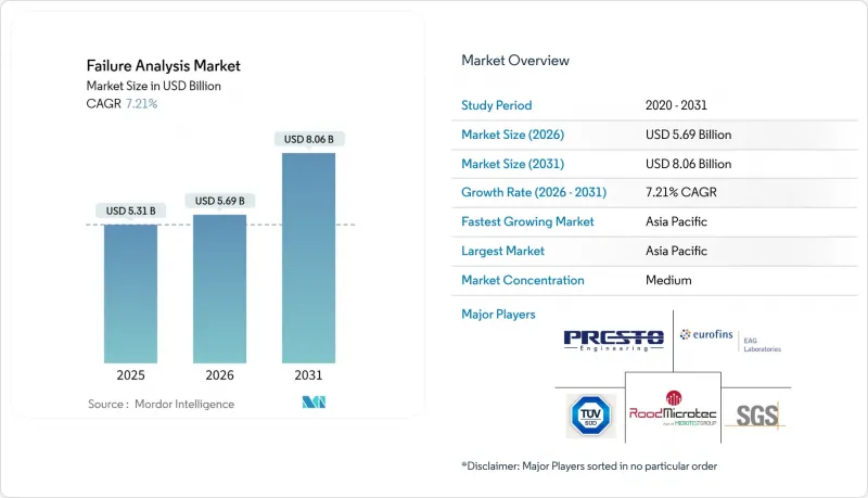
预计故障分析市场将从 2025 年的 53.1 亿美元成长到 2026 年的 56.9 亿美元,到 2031 年将达到 80.5 亿美元,2026 年至 2031 年的复合年增长率为 7.18%。
半导体製造领域对精密诊断的需求不断增长,老化的工业基础设施需要更深入的检测程序,以及传统测试方法分辨率不足的奈米装置的稳步发展,共同推动了半导体产业的持续成长。在美国《晶片製造与资讯安全法案》(CHIPS Act)以及其他国家类似措施的推动下,供应链在地化进程显着加快,促使晶圆厂内部建立分析实验室,并由此催生了对紧凑型自动化工具的相应需求。设备供应商正积极回应,推出双束平台和人工智慧辅助工作流程,以缩短根本原因侦测週期。同时,石油和天然气等资产密集型产业正在采用预测性维护通讯协定,以减少代价高昂的停机时间。亚太地区在政府补贴和密集的晶圆代工厂网络的支持下,仍然是资本投资的中心。北美则正利用政策奖励将产能回流,并加强智慧财产权管理。
全球故障分析市场趋势与洞察
基础设施老化和维护需求不断增加
腐蚀相关的故障每年给石油和天然气行业造成13.72亿美元的损失,促使营运商采用预测性故障分析程序,以便在计划外停机前检测到劣化。深度学习驱动的有限元素模型现已被纳入管道健康管理流程,取代了耗时的人工检查,并缩短了恶劣运作环境的诊断时间。类似的趋势也出现在老化离散製造设备领域,奈米级材料分析正被用于延长设备寿命并防止数百万美元的生产中断。公共产业、炼油厂和交通基础设施所有者正越来越多地将扫描电子显微镜纳入计划维护中,这表明工业资产使用寿命的延长正在推动整个故障分析市场持续增长的需求。
故障分析工具的技术进步
人工智慧辅助影像识别技术如今可在数分钟内分割复杂的缺陷模式,将分析週期从数週缩短至数小时。蔡司展示了一款自动化的交叉光束聚焦离子束扫描电子显微镜(FIB-SEM),可自主处理、成像和分类3D NAND堆迭中的缺陷,将传统週转时间缩短了60%。 TESCAN在台湾的扩张进一步凸显了设备製造商向需要亚10奈米解析度的先进封装技术领域的拓展。设备内建的即时分析功能可实现生产线内製程视窗的即时校正,从而有效地将故障分析从独立实验室转移到生产现场。检测器、离子柱和高亮度光源的进步在不影响分辨率的前提下扩展了视野,并促进了多模态工作流程的实现,从而在一次扫描中集成二次离子和X射线光谱测量。
设备的安装和维修成本高昂
最先进的双束FIB-SEM仪器造价高达数百万美元,需要配备严格环境控制的隔振室。再加上维护、耗材和设备维修的成本,其终身投资金额将会翻倍。预算紧张的公司通常会选择外包,但这可能导致物流延误和保密问题。为了解决这些问题,仪器供应商提案模组化系统、共用设施经营模式和订阅所有权结构,以分散资本支出并普及使用。
细分市场分析
到2025年,二次离子质谱(SIMS)将占据失效分析市场28.85%的份额,主要得益于其掺杂剂分析能力,精度可提升至奈米级。聚焦离子束(FIB)工具的失效分析市场规模预计将以8.36%的复合年增长率成长,这主要受3D装置诊断中对特定位置截面分析的需求所驱动。将SIMS、能量色散X射线光谱(EDX)和飞行时间质谱(TOF-MS)整合于同一阶段的混合平台可缩短工作流程步骤并提高资料相关性。新兴的相对离子蚀刻技术可满足微机电系统(MEMS)和先进材料计划对深度分辨成分分析的需求,且不会产生掩模伪影。未来五年,人工智慧辅助的常规光谱资料解读将使其应用范围扩展至中型晶圆厂,从而扩大SIMS的潜在用户群,同时增强FIB在自动化缺陷隔离方面的优势。
3D封装技术的日益普及也将推动对扫描探针调查方法的需求,尤其是在量子装置开发领域,原子级表面精度至关重要。随着光电进入量产阶段,紫外线雷射辅助二次离子质谱(SIMS)将负责绘製弱讯号缺陷图谱。结合技术多元化,预计这将使失效分析市场保持两位数的设备更新周期,从而建立可持续的投资基础。
区域分析
预计到2025年,亚太地区将占全球收入的46.72%,并在2031年之前以7.89%的复合年增长率增长,这主要得益于该地区集中的晶圆代工厂能力以及旨在实现半导体自给自足的政府补贴。日本已累计3.9兆日圆(约257亿美元)扩大国内产能,将刺激该地区对设备部署和专业服务的需求。儘管面临出口限制的阻力,中国的本土化策略仍在支撑来自国内供应商和国际供应商的需求。韩国在记忆体领域的主导以及台湾在先进逻辑元件领域的主导地位,为下一代分析平台的稳定采购提供了保障。
北美排名第二,《晶片与科学法案》提供的520亿美元津贴和税收优惠鼓励新建晶圆厂在规划阶段就建立内部故障分析实验室。五大湖区和美国西南部电动车供应链的成长进一步推动了该地区对功率元件可靠性研究的需求。欧洲紧追在后,德国的汽车和工业自动化产业丛集的采用率很高。 ISO 9001认证正在推动系统性的缺陷预防流程。在中东和非洲,新的需求正在涌现,主要与石油和天然气管道完整性计划以及在沙乌地阿拉伯「2030愿景」半导体中心计划等框架下构建半导体生态系统的早期倡议有关。虽然南美市场规模仍然小规模,但采矿设备故障诊断和可再生能源组件分析等领域的蓬勃发展正促使跨国工具供应商探索分销合作伙伴关係。
其他福利:
- Excel格式的市场预测(ME)表
- 分析师支持(3个月)
目录
第一章 引言
- 研究假设和市场定义
- 调查范围
第二章调查方法
第三章执行摘要
第四章 市场情势
- 市场概览
- 市场驱动因素
- 基础设施老化和维护需求不断增加
- 故障分析工具的技术进步
- 材料、设计和生产方法的创新
- 电子元件的小型化正在推动需求成长。
- 基于人工智慧的根本原因分析的采用现状
- 供应链本地化促进了企业内部叶酸检测实验室的建立。
- 市场限制
- 设备的购置和拥有成本高昂
- 工厂自动化专业技术人员短缺
- 过长的周转时间会阻碍生产力。
- 智慧财产权保护限制了跨境样本共用。
- 产业价值链分析
- 监管环境
- 技术展望
- 波特五力分析
- 供应商的议价能力
- 买方的议价能力
- 新进入者的威胁
- 替代品的威胁
- 竞争对手之间的竞争
- 对宏观经济趋势的市场评估
第五章 市场规模与成长预测
- 透过技术
- 二次电离质谱法(SIMS)
- 能量色散X射线光谱(EDX)
- 化学机械抛光(CMP)
- 扫描探针显微镜
- 聚焦离子束(FIB)
- 相对离子蚀刻(RIE)
- 其他技术
- 透过装置
- 扫描电子显微镜(SEM)
- 聚焦离子束(FIB)系统
- 穿透式电子显微镜(TEM)
- 双束系统
- 其他设备
- 按最终用户行业划分
- 车
- 石油和天然气
- 防御
- 建造
- 製造业
- 电子装置和半导体
- 其他终端用户产业
- 按地区
- 北美洲
- 我们
- 加拿大
- 墨西哥
- 南美洲
- 巴西
- 阿根廷
- 南美洲其他地区
- 欧洲
- 德国
- 英国
- 法国
- 义大利
- 西班牙
- 其他欧洲
- 亚太地区
- 中国
- 日本
- 印度
- 新加坡
- 澳洲
- 马来西亚
- 亚太其他地区
- 中东和非洲
- 中东
- 沙乌地阿拉伯
- 阿拉伯聯合大公国
- 其他中东地区
- 非洲
- 南非
- 埃及
- 其他非洲地区
- 中东
- 北美洲
第六章 竞争情势
- 市场集中度
- 策略趋势
- 市占率分析
- 公司简介
- Presto Engineering Inc.
- TUV SUD
- Rood Microtec GmbH
- Eurofins EAG Laboratories
- SGS SA
- CoreTest Technologies Inc.
- Materials Testing Inc.
- McDowell Owens Engineering Inc.
- Exponent Inc.
- TechInsights Inc.
- Hitachi High-Tech Analytical Science Ltd.
- Intertek Group plc
- NanoScope Services Ltd
- Applus+Laboratories Inc.
- Advanced Nanolab Pte Ltd
- Toray Engineering Co., Ltd.
- Tescan Orsay Holding
- Leica Microsystems Inc.
- Keysight Technologies Inc.
- Crane Engineering Inc.
第七章 市场机会与未来展望
The Failure Analysis market is expected to grow from USD 5.31 billion in 2025 to USD 5.69 billion in 2026 and is forecast to reach USD 8.05 billion by 2031 at 7.18% CAGR over 2026-2031.
Persistent growth rests on rising precision-diagnostics demand in semiconductor manufacturing, aging industrial infrastructure that mandates deeper inspection routines, and the steady shift to nanoscale devices where conventional test methods lose resolution. Intensifying supply-chain localization, most visibly under the U.S. CHIPS Act and similar initiatives elsewhere, accelerates in-house analytical-lab adoption inside fabs, creating parallel demand for compact, automated tools. Equipment vendors are responding with dual-beam platforms and AI-assisted workflows that shorten root-cause cycles, while asset-heavy sectors such as oil and gas adopt predictive protocols to curb costly downtime events. Asia-Pacific remains the epicenter of capital expenditure, helped by government subsidies and its dense foundry network, whereas North America leverages policy incentives to reshore capacity and tighten intellectual-property control.
Global Failure Analysis Market Trends and Insights
Ageing Infrastructure and Increasing Maintenance Needs
Corrosion-related failures cost the oil and gas sector USD 1.372 billion each year, a burden that is steering operators toward predictive failure analysis programs that detect degradation before unplanned shutdowns. Deep-learning-enabled finite-element models are now embedded into pipeline-integrity routines, replacing slower manual inspections and cutting diagnostic time in harsh operating zones. Similar patterns appear in aging discrete-manufacturing equipment, where nanoscale materials analysis helps extend tool life and prevent multi-million-dollar production halts. Utilities, refineries, and transportation infrastructure owners increasingly embed scanning-electron-microscopy checks in scheduled maintenance, illustrating how industrial asset longevity fuels recurring demand across the failure analysis market.
Technological Advancements in Failure-Analysis Tools
AI-assisted image-recognition now segments complex defect patterns in minutes, slashing analysis-cycle time from weeks to hours. ZEISS demonstrated an automated Crossbeam FIB-SEM that can autonomously mill, image, and classify faults in 3D NAND stacks, shaving 60% off typical turnaround schedules. TESCAN's expansion in Taiwan further underscores toolmakers' push into advanced-packaging nodes that require resolution below 10 nm. Real-time analytics embedded directly on the tool allow immediate process-window corrections inside fab lines, effectively relocating failure analysis from separate laboratories to production floors. Advancements in detectors, ion columns, and high-brightness sources also extend the field-of-view without compromising resolution, fostering multimodal workflows that merge secondary-ion and X-ray spectrometry in a single pass.
High Acquisition and Ownership Cost of Equipment
A state-of-the-art dual-beam FIB-SEM can command several million USD and requires vibration-isolated rooms with strict environmental controls, doubling the lifetime investment once maintenance, consumables, and facility retrofits are factored in. Budget-constrained enterprises often resort to outsourcing, introducing logistics delays and potential confidentiality issues. Tool vendors are countering with modular systems, shared-facility business models, and subscription-based ownership structures that spread capital outlays and democratize access.
Other drivers and restraints analyzed in the detailed report include:
- Innovation in Materials, Design and Production Methods
- Miniaturization of Electronic Components Boosts Demand
- Shortage of Skilled Failure Analysis Professionals
For complete list of drivers and restraints, kindly check the Table Of Contents.
Segment Analysis
SIMS held 28.85% of the failure analysis market share in 2025, favored for dopant-profiling accuracy that scales into single-digit nanometers. The failure analysis market size tied to Focused Ion Beam tools is on course for an 8.36% CAGR, propelled by demand for site-specific cross-sectioning during 3D-device diagnostics. Hybrid platforms that merge SIMS, EDX, and time-of-flight mass spectrometry on the same stage now shorten workflow steps and improve data correlation. Emerging Relative Ion Etching complements MEMS and advanced-materials projects that need depth-resolved compositional profiling without masking artifacts. Over the next five years, AI-assisted routine-spectra interpretation will extend usability to mid-tier fabs, expanding the addressable base for SIMS while reinforcing FIB traction in automated defect isolation.
Wider 3D packaging adoption also lifts scanning-probe methodologies, especially for quantum-device development that hinges on atomic-scale surface fidelity. As photonics-integrated circuits enter mass production, ultraviolet laser-assisted SIMS steps in to map low-signal defects. Collectively, technology diversification will sustain double-digit tool refresh cycles and anchor continuous investment in the failure analysis market.
The Failure Analysis Market Report is Segmented by Technology (Secondary ION Mass Spectrometry, Energy Dispersive X-Ray Spectroscopy, and More), Equipment (Scanning Electron Microscope, Focused Ion Beam System, and More), End-User Industry (Automotive, Oil and Gas, and More), and Geography (North America, South America, Europe, Asia-Pacific, and Middle East and Africa). The Market Forecasts are Provided in Terms of Value (USD).
Geography Analysis
Asia-Pacific held 46.72% of global revenue in 2025 and is forecast to grow at 7.89% CAGR through 2031, bolstered by concentrated foundry capacity and national subsidies that target semiconductor self-sufficiency. Japan earmarked JPY 3.9 trillion (USD 25.7 billion) to lift domestic output, sparking a surge in regional tool installations and specialized-service inquiries. China's localization strategy keeps domestic tool vendors and overseas suppliers occupied, even amid export-control headwinds. South Korea's memory leadership and Taiwan's advanced-logic dominance reinforce steady procurement of next-generation analytical platforms.
North America ranks second as the CHIPS and Science Act allocates USD 52 billion in grants and tax incentives, motivating new fabs that embed in-house failure analysis laboratories during planning phases. Electric-vehicle supply-chain growth around the Great Lakes and U.S. Southwest further increases regional demand for power-device reliability studies. Europe follows with strong adoption in Germany's automotive and industrial-automation clusters, where ISO 9001 compliance drives systematic defect-prevention cycles. Middle East and Africa exhibit emerging traction, primarily tied to oil-and-gas pipeline integrity programs and early moves to build semiconductor ecosystems under policy umbrellas such as Saudi Arabia's Vision 2030 semiconductor hub. South America remains a smaller market but shows promise in mining-equipment fault diagnostics and renewable-energy component analysis, leading multinational tool vendors to explore distributor partnerships
- Presto Engineering Inc.
- TUV SUD
- Rood Microtec GmbH
- Eurofins EAG Laboratories
- SGS SA
- CoreTest Technologies Inc.
- Materials Testing Inc.
- McDowell Owens Engineering Inc.
- Exponent Inc.
- TechInsights Inc.
- Hitachi High-Tech Analytical Science Ltd.
- Intertek Group plc
- NanoScope Services Ltd
- Applus+ Laboratories Inc.
- Advanced Nanolab Pte Ltd
- Toray Engineering Co., Ltd.
- Tescan Orsay Holding
- Leica Microsystems Inc.
- Keysight Technologies Inc.
- Crane Engineering Inc.
Additional Benefits:
- The market estimate (ME) sheet in Excel format
- 3 months of analyst support
TABLE OF CONTENTS
1 INTRODUCTION
- 1.1 Study Assumptions and Market Definition
- 1.2 Scope of the Study
2 RESEARCH METHODOLOGY
3 EXECUTIVE SUMMARY
4 MARKET LANDSCAPE
- 4.1 Market Overview
- 4.2 Market Drivers
- 4.2.1 Ageing infrastructure and increasing maintenance needs
- 4.2.2 Technological advancements in failure-analysis tools
- 4.2.3 Innovation in materials, design and production methods
- 4.2.4 Miniaturisation of electronic components boosts demand
- 4.2.5 AI-driven root-cause analytics adoption
- 4.2.6 Supply-chain localization spurs in-house FA labs
- 4.3 Market Restraints
- 4.3.1 High acquisition and ownership cost of equipment
- 4.3.2 Shortage of skilled FA professionals
- 4.3.3 Long turnaround time hampers productivity
- 4.3.4 IP-protection limits cross-border sample sharing
- 4.4 Industry Value Chain Analysis
- 4.5 Regulatory Landscape
- 4.6 Technological Outlook
- 4.7 Porter's Five Forces Analysis
- 4.7.1 Bargaining Power of Suppliers
- 4.7.2 Bargaining Power of Buyers
- 4.7.3 Threat of New Entrants
- 4.7.4 Threat of Substitutes
- 4.7.5 Intensity of Competitive Rivalry
- 4.8 Assessment of Macro-economic Trends on the Market
5 MARKET SIZE AND GROWTH FORECASTS (VALUE)
- 5.1 By Technology
- 5.1.1 Secondary ION Mass Spectrometry (SIMS)
- 5.1.2 Energy Dispersive X-ray Spectroscopy (EDX)
- 5.1.3 Chemical Mechanical Planarization (CMP)
- 5.1.4 Scanning Probe Microscopy
- 5.1.5 Focused Ion Beam (FIB)
- 5.1.6 Relative Ion Etching (RIE)
- 5.1.7 Other Technologies
- 5.2 By Equipment
- 5.2.1 Scanning Electron Microscope (SEM)
- 5.2.2 Focused Ion Beam (FIB) System
- 5.2.3 Transmission Electron Microscope (TEM)
- 5.2.4 Dual Beam System
- 5.2.5 Other Equipment's
- 5.3 By End-user Industry
- 5.3.1 Automotive
- 5.3.2 Oil and Gas
- 5.3.3 Defense
- 5.3.4 Construction
- 5.3.5 Manufacturing
- 5.3.6 Electronics and Semiconductors
- 5.3.7 Other End-user Industries
- 5.4 By Geography
- 5.4.1 North America
- 5.4.1.1 United States
- 5.4.1.2 Canada
- 5.4.1.3 Mexico
- 5.4.2 South America
- 5.4.2.1 Brazil
- 5.4.2.2 Argentina
- 5.4.2.3 Rest of South America
- 5.4.3 Europe
- 5.4.3.1 Germany
- 5.4.3.2 United Kingdom
- 5.4.3.3 France
- 5.4.3.4 Italy
- 5.4.3.5 Spain
- 5.4.3.6 Rest of Europe
- 5.4.4 Asia-Pacific
- 5.4.4.1 China
- 5.4.4.2 Japan
- 5.4.4.3 India
- 5.4.4.4 Singapore
- 5.4.4.5 Australia
- 5.4.4.6 Malaysia
- 5.4.4.7 Rest of Asia-Pacific
- 5.4.5 Middle East and Africa
- 5.4.5.1 Middle East
- 5.4.5.1.1 Saudi Arabia
- 5.4.5.1.2 United Arab Emirates
- 5.4.5.1.3 Rest of Middle East
- 5.4.5.2 Africa
- 5.4.5.2.1 South Africa
- 5.4.5.2.2 Egypt
- 5.4.5.2.3 Rest of Africa
- 5.4.5.1 Middle East
- 5.4.1 North America
6 COMPETITIVE LANDSCAPE
- 6.1 Market Concentration
- 6.2 Strategic Moves
- 6.3 Market Share Analysis
- 6.4 Company Profiles (includes Global level Overview, Market level overview, Core Segments, Financials as available, Strategic Information, Market Rank/Share for key companies, Products and Services, and Recent Developments)
- 6.4.1 Presto Engineering Inc.
- 6.4.2 TUV SUD
- 6.4.3 Rood Microtec GmbH
- 6.4.4 Eurofins EAG Laboratories
- 6.4.5 SGS SA
- 6.4.6 CoreTest Technologies Inc.
- 6.4.7 Materials Testing Inc.
- 6.4.8 McDowell Owens Engineering Inc.
- 6.4.9 Exponent Inc.
- 6.4.10 TechInsights Inc.
- 6.4.11 Hitachi High-Tech Analytical Science Ltd.
- 6.4.12 Intertek Group plc
- 6.4.13 NanoScope Services Ltd
- 6.4.14 Applus+ Laboratories Inc.
- 6.4.15 Advanced Nanolab Pte Ltd
- 6.4.16 Toray Engineering Co., Ltd.
- 6.4.17 Tescan Orsay Holding
- 6.4.18 Leica Microsystems Inc.
- 6.4.19 Keysight Technologies Inc.
- 6.4.20 Crane Engineering Inc.
7 MARKET OPPORTUNITIES AND FUTURE OUTLOOK
- 7.1 White-space and Unmet-Need Assessment
 2026年全球失效分析市场报告
 故障调查服务市场:依服务模式、调查方法、组件类型、产业垂直领域和最终用户划分-2026-2032年全球预测按产品类型、最终用户、分销管道、应用和技术分類的故障分析市场 - 全球预测 2025-2032
 全球失效分析与测试设备市场:市场规模、份额和趋势分析(按产品、技术、应用和地区划分),细分市场预测(2025-2033 年)
 2025 年至 2033 年故障分析市场规模、份额、趋势及预测(按设备、最终用途、产业及地区)
 故障分析市场:2025-2030 年预测半导体故障分析设备市场规模、份额、趋势分析报告:产品、技术、地区、细分市场预测,2025-2030
 故障分析设备市场规模、份额、成长分析,按设备类型、按技术、按应用、按最终用户、按地区 - 行业预测,2025 年至 2032 年故障分析市场规模、份额、趋势分析报告:2024-2030 年按设备、技术、产业、地区和细分市场进行的预测