


 |
市场调查报告书
商品编码
1630220
记忆体封装:市场占有率分析、产业趋势与统计、成长预测(2025-2030)Memory Packaging - Market Share Analysis, Industry Trends & Statistics, Growth Forecasts (2025 - 2030) |
||||||
※ 本网页内容可能与最新版本有所差异。详细情况请与我们联繫。
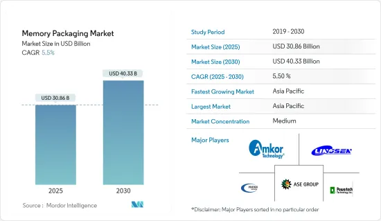
记忆体封装市场规模预计到 2025 年为 308.6 亿美元,预计到 2030 年将达到 403.3 亿美元,预测期内(2025-2030 年)复合年增长率为 5.5%。
最近的COVID-19疫情预计将导致受访市场供应链出现严重失衡,其中亚太地区,尤其是中国,是受访市场的主要影响因素之一。此外,亚太地区许多地方政府正在对半导体产业进行长期投资,因此预计将恢復市场成长。例如,中国政府已为国家积体电路投资基金2030年第二期筹集约230亿至300亿美元。全球多个地区的经济影响对半导体市场的成长构成重大挑战,因为市场从疫情中恢復的时间尚不确定,而先进记忆体封装市场所需的关键原材料的供应预计将直接影响半导体市场的成长。全球性别的影响。
主要亮点
- 记忆体采用多种封装技术,包括覆晶、导线架、引线键合和硅通孔 (TSV)。随着晶片变得更小、更复杂,与外部电路的电气连接数量也随之增加。
- 这也带动了封装技术的发展。覆晶、TSV 和晶圆级晶片级封装 (WLCSP) 是很有前途的技术,可满足宽频化、高速和更小/更薄封装的需求。易于理解的程式调整、低工程成本和轻鬆转换正在推动对打线接合记忆体封装平台的需求。
- 此外,随着封装设计的变化,引线键合记忆体平台由于其灵活性、可靠性和低成本而继续被用作最优选的互连平台。覆晶于 2016 年开始进入 DRAM 记忆体封装领域,并且由于高频宽需求推动 DRAM PC/伺服器的采用增加,预计倒装晶片将会成长。
- 记忆体晶片的高频宽和低延迟正在推动许多应用中对高效能运算的需求,高频宽记忆体正在采用硅穿孔电极(TSV)。
记忆体封装市场趋势
DRAM预计将占据较大份额
- 市场正在见证移动和计算(主要是伺服器)的需求。每支智慧型手机的 DRAM 记忆体容量预计将平均增加三倍以上,到 2022 年达到约 6GB。
- 最近,研究市场的主导厂商之一三星电子宣布批量生产用于高阶智慧型手机的新型记忆体封装。
- 对于行动应用,引线键合平台预计将主导记忆体封装。然而,高阶智慧型手机向多晶片封装(ePoP)的过渡可能很快就会开始。随着企业架构和云端运算的改进,运算 DRAM 封装预计将在预测期内显着成长。
- 三星的 HBM2 技术由 8 个 8Gbit DRAM晶粒组成,使用 5,000 个 TSV 堆迭在一起。最近,该公司还发布了新的 HBM 版本,可堆迭 12 个 DRAM晶粒,并使用 60,000 个 TSV 将它们连接起来。
- 每部智慧型手机的 DRAM 记忆体容量正在增加,新装置至少提供 4GB 容量,预计到 2020 年将达到至少 6GB 至 8GB 容量。每部智慧型手机的 NAND 容量正在不断增加,目前已超过 64GB,预计到 2020 年将达到 150GB 以上。对于伺服器而言,到 2020 年,每台伺服器的 DRAM 容量预计将增加到约 1TB,而企业级 SSD NAND 容量预计到预测期结束时将达到 5TB 以上。
汽车工业占有很大份额
- 在自动驾驶和车载资讯娱乐趋势的推动下,使用低密度(低 MB)记忆体的汽车市场可能会增加 DRAM 记忆体的采用。由于触控显示器驱动IC、AMOLED显示器和工业IoT等新领域的应用,NOR快闪记忆体封装市场预计也将成长。
- 作为其成长策略的一部分,许多 OSAT 厂商已与记忆体晶片製造商建立策略联盟,而区域厂商正在与全球技术供应商合作,以扩大其市场影响力。
- 市场上的製造商正在扩大其生产设施。例如,SK海力士公司正在扩大其在韩国的半导体封装和测试设施的产能。这些发展可能会增加现有参与者的市场开发机会,并为竞争对手提供市场优势。
- 封装技术中引入的创新与大型系统晶片(SoC) 解决方案中功能密度的增加有关。然而,汽车环境中严格的可靠性要求和 OSAT 行业不断变化的模式预计将阻碍预测期内的市场成长。
- 最近,硅基感测器技术在生物辨识感测器、CMOS 影像感测器和加速计等 MEMS 感测器等各种应用中的使用有所增加。此外,整合到行动装置(例如行动电话和 PDA)中的感测器装置的数量正在增加。对于这些应用,小尺寸、低成本且易于整合对于成功整合此感测器技术至关重要。
- 一般来说, OEM更喜欢即插即用模组或完整的子系统,这也是帮助储存晶片市场的一个因素,进而带动储存封装需求以增强技术应用。
记忆体封装产业概况
记忆体封装市场的竞争是温和的。随着DRAM记忆体价格的上涨,记忆体封装市场的供应商正在增加在3D NAND开发上的投入。根据SK海力士公司发表的报导,各公司已无法满足3D NAND的需求,并被要求扩大其製造能力。此外,许多公司正在扩大其製造设备以满足不断增长的需求。总体而言,在预测期内,由于上述所有因素,市场可能会转向高度竞争。
其他好处:
- Excel 格式的市场预测 (ME) 表
- 3 个月分析师支持
目录
第一章简介
- 研究假设和市场定义
- 调查范围
第二章调查方法
第三章执行摘要
第四章市场动态
- 市场概况
- 产业吸引力-波特五力分析
- 供应商的议价能力
- 消费者议价能力
- 新进入者的威胁
- 替代品的威胁
- 竞争公司之间的敌对关係
- 产业价值链分析
- 技术蓝图
- COVID-19 市场影响评估
- 市场驱动因素
- 自动驾驶和车载资讯娱乐新趋势
- 智慧型手机需求增加
- 储存半导体业务爆发式成长
- 持续开发高频宽记忆体 (HBM) 和重新分配层
- 市场挑战
- 汽车环境中严格的可靠性要求
- OSAT产业模式的变化
第五章市场区隔
- 按平台
- 覆晶
- 导线架
- 晶圆级晶片级封装 (WLCSP)
- 硅穿孔电极(TSV)
- 焊接线
- 按用途
- NAND快闪记忆体封装
- NOR快闪记忆体封装
- DRAM封装
- 其他应用
- 按最终用户产业
- 资讯科技和电信
- 消费性电子产品
- 车
- 其他最终用户产业
- 按地区
- 北美洲
- 欧洲
- 亚太地区
- 世界其他地区
第六章 竞争状况
- 公司简介
- Tianshui Huatian Technology Co. Ltd
- Hana Micron Inc.
- Lingsen precision industries Ltd
- Formosa Advanced Technologies Co. Ltd(Nanya Technology Corporation)
- Advanced Semiconductor Engineering Inc.(ASE Inc.)
- Amkor Technology Inc.
- Powertech Technology Inc.
- Jiangsu Changjiang Electronics Technology Co. Ltd
- Powertech Technology Inc.
- King Yuan Electronics Corp. Ltd
- ChipMOS Technologies Inc.
- TongFu Microelectronics Co.
- Signetics Corporation
第七章 投资分析
第八章市场的未来
The Memory Packaging Market size is estimated at USD 30.86 billion in 2025, and is expected to reach USD 40.33 billion by 2030, at a CAGR of 5.5% during the forecast period (2025-2030).
The recent COVID-19 outbreak is expected to create significant imbalances in the supply chain of the market studied, as Asia-Pacific, particularly China, is one of the major influencers of the market studied. Also, many of the local governments in the Asia-Pacific have invested in the semiconductor industry in a long run program, hence, expected to regain market growth. For instance, the Chinese government raised around USD 23 to 30 billion funds, to pay for the second phase of its National IC Investment Fund 2030. Owing to the uncertainty in the recovery time of the market from the pandemic, economic impacts on several parts of the world are further expected to provide significant challenges to the growth of the semiconductor market, directly affecting the availability of critical raw materials required for advanced memory packaging market globally.
Key Highlights
- Memory devices employed a broad range of the packaging technology that include flip-chip, lead-frame, wire-bond, through-silicon via (TSV). With the decrease in dimensions and increase in the chip functionality, a higher number of the electrical connections have to be made to the external circuit.
- This has also led to development in packaging technologies. Flip-chip, TSV, and wafer-level chip-scale Packaging (WLCSP) are promising technologies to satisfy wider bandwidth, faster speed, and smaller/thinner package. Comprehensible program adjustments, low engineering costs, and easy changeovers are fueling the demand for the wire-bond memory packaging platform.
- Additionally, due to changes in the package design, the wire-bond memory packaging platform continues to be used as the most preferred interconnection platform because of its flexibility, reliability, and low-cost. Flip-chip began making inroads in the DRAM memory packaging in 2016 and was expected to grow due to its increased adoption in the DRAM PC/server, fueled by high bandwidth requirements.
- Spurred on by high bandwidth and memory chips' low latency demands for high-performance computing in numerous applications, through-silicon via (TSV), is being employed in high bandwidth memory devices.
Memory Packaging Market Trends
DRAM is Estimated to Hold Significant Share
- The market studied is witnessing demand from mobile and the computing (mainly servers). On average, the DRAM memory capacity per smartphone is anticipated to rise more than threefold to reach around 6GB by 2022.
- Recently, Samsung Electronics Co. Ltd, one of the dominant players in the market studied, announced the mass production of the new memory package aimed at high-end smartphones, which may save space by putting DRAM and eMMC together.
- For mobile applications, memory packaging is expected to remain on the wire-bond platform mostly. However, it will soon begin moving toward the multi-chip package (ePoP) for high-end smartphones. With the improvement in enterprise architecture and cloud computing, the computing DRAM packaging is anticipated to witness significant growth during the forecast period.
- Samsung's HBM2 technology consists of eight 8Gbit DRAM dies, which are stacked and connected using 5,000 TSVs. Recently, the company also launched a new HBM version that stacks 12 DRAM dies, which are connected using 60,000 TSVs and are ideal for data-intensive applications, such as AI and HPC.
- DRAM memory capacity per smartphone has risen with new devices offering a minimum of 4 Gb space which is expected to reach a minimum of 6 GB to 8 GB of space by 2020, while NAND capacity per smartphone has increased reaching more than 64 GB now and are expected to become reach over 150 GB by 2020. For servers, DRAM capacity per unit is projected to increase to approximately 1 TB by 2020 and NAND capacity for each SSD for the enterprise market are expected to reach more than 5 TB in capacity by the end of the forecast period
Automotive Industry to Hold Significant Share
- The automotive market, which uses the low density (low-MB) memory, might observe an increase in the acceptance of DRAM memory, led by the growing trend of autonomous driving and in-vehicle infotainment. NOR Flash memory packaging market is also expected to grow due to its application in new areas, such as touch display driver ICs, AMOLED display, and industrial IoTs.
- As part of the growth strategy, numerous OSAT players are entering into strategic alliances with memory chip manufacturers, and regional players are partnering with global technology providers to increase their reach in the market.
- Manufacturers operating in the market are expanding their production facilities. For instance, SK Hynix Inc. is expanding its semiconductor packaging and inspection facility capacity in South Korea. Such developments are expected to help create increased opportunity for the existing players and cut competitors edge in the market studied.
- The innovations being introduced in the packaging technology are associated with the growth in functional density of large system-on-chip (SoC) solutions. However, harsh reliability requirements in the automotive environment and changing landscape of the OSATs industry is anticipated to hamper the growth of the market studied over the forecast period.
- In recent times, there has been growth in the use of Si-based sensor technology for a variety of applications, including biometric sensors, CMOS image sensors, and MEMS sensors, such as accelerometers. Increasingly, and sensor devices are being integrated into portable devices, like handsets and PDAs. In these applications, small-size, low-cost, and ease-of-integration are essential to incorporate this sensor technology successfully.
- Generally, OEMs prefer a plug-and-play module or complete subsystem, which is also a factor that is helping the memory chip market, and in turn, driving the demand for the memory packaging for enhanced technological applications.
Memory Packaging Industry Overview
The memory packaging market is moderately competitive. With the rising prices of DRAM memory, vendors operating in the memory packaging market are increasingly spending on the development of 3D NAND. According to an article published by SK Hynix Inc., companies can no longer keep up with 3D NAND demand and are required to expand their manufacturing capacity. Also, many of the companies are expanding their manufacturing units in order to meet the growing demand. Overall the market might move towards highly competitive during the forecast period due to all the above factors.
Additional Benefits:
- The market estimate (ME) sheet in Excel format
- 3 months of analyst support
TABLE OF CONTENTS
1 INTRODUCTION
- 1.1 Study Assumptions and Market Definition
- 1.2 Scope of the Study
2 RESEARCH METHODOLOGY
3 EXECUTIVE SUMMARY
4 MARKET DYNAMICS
- 4.1 Market Overview
- 4.2 Industry Attractiveness - Porter's Five Forces Analysis
- 4.2.1 Bargaining Power of Suppliers
- 4.2.2 Bargaining Power of Consumers
- 4.2.3 Threat of New Entrants
- 4.2.4 Threat of Substitutes
- 4.2.5 Intensity of Competitive Rivalry
- 4.3 Industry Value Chain AnalysiS
- 4.4 Technology RoadmaP
- 4.5 Assessment of Impact of COVID-19 on the Market
- 4.6 Market Drivers
- 4.6.1 Emerging Trend of Autonomous Driving and In-vehicle Infotainment
- 4.6.2 Increase in Demand for Smartphones
- 4.6.3 Memory Semiconductor Business Explosion
- 4.6.4 Continuous Developments in High-bandwidth Memory (HBM) and Redistribution Layer
- 4.7 Market Challenges
- 4.7.1 Harsh Reliability Requirements in the Automotive Environment
- 4.7.2 Changing Landscape of the OSATs Industry
5 MARKET SEGMENTATION
- 5.1 By Platform
- 5.1.1 Flip-chip
- 5.1.2 Lead-frame
- 5.1.3 Wafer-level Chip-scale Packaging(WLCSP)
- 5.1.4 Through-silicon Via (TSV)
- 5.1.5 Wire-bond
- 5.2 By Application
- 5.2.1 NAND Flash Packaging
- 5.2.2 NOR Flash Packaging
- 5.2.3 DRAM Packaging
- 5.2.4 Other Applications
- 5.3 By End-user Industry
- 5.3.1 IT and Telecom
- 5.3.2 Consumer Electronics
- 5.3.3 Automotive
- 5.3.4 Other End-user Industries
- 5.4 Geography
- 5.4.1 North America
- 5.4.2 Europe
- 5.4.3 Asia-Pacific
- 5.4.4 Rest of the World
6 COMPETITIVE LANDSCAPE
- 6.1 Company Profiles
- 6.1.1 Tianshui Huatian Technology Co. Ltd
- 6.1.2 Hana Micron Inc.
- 6.1.3 Lingsen precision industries Ltd
- 6.1.4 Formosa Advanced Technologies Co. Ltd (Nanya Technology Corporation)
- 6.1.5 Advanced Semiconductor Engineering Inc. (ASE Inc.)
- 6.1.6 Amkor Technology Inc.
- 6.1.7 Powertech Technology Inc.
- 6.1.8 Jiangsu Changjiang Electronics Technology Co. Ltd
- 6.1.9 Powertech Technology Inc.
- 6.1.10 King Yuan Electronics Corp. Ltd
- 6.1.11 ChipMOS Technologies Inc.
- 6.1.12 TongFu Microelectronics Co.
- 6.1.13 Signetics Corporation
