 |
市场调查报告书
商品编码
1632032
欧洲半导体蚀刻设备:市场占有率分析、产业趋势/统计、成长预测(2025-2030)Europe Semiconductor Etch Equipment - Market Share Analysis, Industry Trends & Statistics, Growth Forecasts (2025 - 2030) |
||||||
价格
※ 本网页内容可能与最新版本有所差异。详细情况请与我们联繫。
简介目录
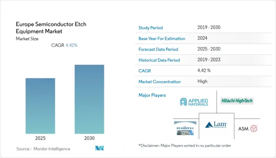
欧洲半导体蚀刻设备市场预计在预测期内复合年增长率为4.42%

主要亮点
- 欧洲半导体蚀刻设备市场依赖扩大内部半导体製造来避免全球供应链缺口。欧盟正在考虑在欧洲建造先进的半导体工厂,以避免依赖美国和亚洲的半导体及外围元件供应。欧盟正在探索生产尺寸小于 10 奈米的半导体的方法,最终缩小到 2 奈米晶片。例如,欧盟宣布了针对半导体的重大补贴制度,目标是根据《欧盟晶片法案》,到2030年动员430亿欧元的公共和私人投资用于半导体研究、设计和生产。
- 作为新兴经济体,该地区的 5G 无线系统、联网汽车和高效能运算市场正在强劲成长。由于半导体的使用对于上述所有市场都至关重要,因此该地区的半导体蚀刻设备市场正在间接成长。例如,化合物半导体行业等离子体处理设备的领先供应商Samco宣布在列支敦士登的Samco-ucp ltd安装电浆蚀刻系统和UV臭氧清洗系统。
- 欧洲的工业自动化也正在推动欧洲半导体製造业的成长。例如,英特尔选择德国作为大型新晶片製造基地的所在地,这是整个欧洲 880 亿美元投资计划中的首个项目,旨在减少对进口的依赖并缓解製造商的供不应求。 。
- 出于多种原因,原材料和零件的来源正在转移到欧盟之外,包括为了避免遵守 REACH(法规和授权)等严格的环境法规。原料加工厂和零件製造搬迁到欧盟之外,破坏了欧盟某些地区现有供应链的稳定。建构新的供应商生态系统增加了晶片製造商的业务支出,并增加了供应商的不确定性。此外,对该地区某些化合物的使用限制也会限制设计灵活性和创新潜力。这些都是欧洲半导体蚀刻设备市场成长的挑战。
- COVID-19 对欧洲半导体蚀刻设备市场产生了负面影响,导致半导体产业的供应链和生产中断。劳动力短缺对半导体蚀刻设备製造商的影响尤其严重。疫情期间,全球半导体供应链中的公司被迫缩减或取消营运。由于汽车等行业需要半导体,该领域出现了严重的亏损和需求的增加,导致该地区供应链出现巨大缺口。
欧洲半导体蚀刻设备市场趋势
该市场是由政府和欧盟晶片法案战略推动的,该战略正在促进半导体和外围产品的内部生产,以避免全球供应链缺口。
- 《欧洲晶片法案》旨在提高欧洲在半导体技术和应用方面的竞争力和弹性,并加速该地区的数位化和绿色转型。为了实现该地区的可持续成长,欧盟正在规划发展该地区整个价值链的蓝图,其中包括半导体蚀刻设备製造商。该地区许多国家开始接受这项策略。例如,英国政府正在寻求业界对国内半导体产业和晶片供给能力状况的回馈。
- 德国经济部长宣布,德国愿意向「欧洲通用利益关键计划」投资 30 亿欧元,这是欧盟刺激投资和减少对进口依赖的关键补贴工具。德国政府打算用这笔钱建造新的半导体製造工厂。这项投资的重点是减少未来半导体需求对进口的依赖。
- 大学、政府和企业正在共同努力开发该地区半导体的新蚀刻技术。例如,威尔斯政府正在资助一个由斯旺西大学主导的计划,并与合作伙伴合作开发世界领先的半导体製程技术。应用范例包括自动驾驶汽车、新型清洁能源设备、未来移动、人工智慧、先进封装、生物感测器和可穿戴感测器。 SPTS Technologies(KLA 公司)、IQE、化合物半导体中心 (CSC)、Biovici、BioMEMS、斯旺西大学和卡迪夫大学以及整合化合物半导体有限公司是 ASSET(专用半导体蚀刻)的少数合作伙伴。
- 该地区正在发展半导体及相关领域的内部製造。在欧洲,政府的支持措施正在增加对新兴企业的资助。例如,Almi Invest 在 AlixLabs 投入了约 300 万瑞典克朗,该公司正在研究使半导体元件更便宜、更快的新方法。瑞典隆德的 AlixLab 发明了原子层蚀刻间距分裂,这是一种用于半导体元件製造的革命性新技术,消除了製造过程中的许多步骤。
多功能先进半导体晶片在工业自动化中的应用正在推动该地区的半导体蚀刻设备市场。
- 欧洲公司正在透过跨产业引入自动化进行转型。半导体的应用在这一自动化过程中至关重要,并且正在推动该地区的半导体蚀刻设备市场。在欧盟,产业联盟是半导体技术和处理器领域的趋势。
- 此次合作的目的是确定现有差距和所需的技术发展,以提高欧盟半导体产业(特别是欧洲中小企业)的公司和研发机构的竞争力。在密集型产业中,这种合作有助于组织克服进入障碍、达到临界点并减少依赖。
- 许多全球半导体製造商都有兴趣在欧洲开发高性能工业半导体。例如,英飞凌科技公司宣布将在奥地利菲拉赫的新晶片工厂开始生产,该工厂也是功率半导体能力中心。英飞凌科技公司在这里开发了 300 毫米厚晶圆的功率半导体製造,后来在德国德勒斯登扩展到全自动化大规模生产。这种製造设备需要蚀刻设备,这将直接或间接扩大欧洲半导体蚀刻设备市场。
- 具有新兴技术功能的半导体是工业自动化的组成部分。该地区大力投资生产高科技半导体製造设备。例如,德国工程技术公司博世在德勒斯登建成了一座新的半导体工厂,该工厂完全采用5G行动技术连网。博世在这座高科技设施上投资了约 10 亿欧元,成为其 130 年历史上最大的单笔投资。各种半导体蚀刻设备是製造半导体晶片不可或缺的。
欧洲半导体蚀刻设备产业概况
由于少数参与企业主导市场,半导体蚀刻设备市场趋势已巩固。进入这个市场需要大量资金,这为新进入者设置了障碍。主要企业正专注于产品创新、併购等策略,以确保在欧洲市场占有较大份额。
- 2022 年 3 月:英特尔投资约 130 亿美元改善扩建其位于爱尔兰莱克斯利普的工厂。英特尔计划在升级后的工厂支援Intel4製程(以前称为7nm)。该计划目前正在进行中,预计将于 2023 年开始生产。
- 2022 年 4 月:3M 位于比利时的半导体冷却剂工厂无限期关闭。该工厂占全球半导体冷却剂产量的80%。
- 2022 年 6 月:义大利电力测试设备製造商 Colllaudi Elettronici Automatizzati 被日本 Advantest (CREA) 收购。 CREA 是一家领先的供应商,在设计和製造功率半导体测试设备方面拥有丰富的经验。此次收购将使 Advantest 能够为高成长产业中更广泛的客户提供更广泛的测试和测量解决方案。
其他好处
- Excel 格式的市场预测 (ME) 表
- 3 个月分析师支持
目录
第一章简介
- 研究成果
- 研究场所
- 调查范围
第二章调查方法
第三章执行摘要
第四章市场动态
- 市场概况
- 市场驱动因素
- 政府和欧盟针对半导体及外围产品内部生产的晶片法战略,以避免全球供应链缺口
- 多功能先进半导体晶片在工业自动化的应用
- 市场限制因素
- 建构区域供应商生态系统
- 价值链分析
- 波特五力分析
- 新进入者的威胁
- 买家/消费者的议价能力
- 供应商的议价能力
- 替代品的威胁
- 竞争公司之间敌对关係的强度
- COVID-19 对市场的影响
第五章市场区隔
- 依产品类型
- 高密度蚀刻设备
- 低密度蚀刻设备
- 依蚀刻类型
- 导体蚀刻
- 介电蚀刻
- 多晶硅蚀刻
- 按用途
- 逻辑和记忆
- 功率元件
- MEMS
- 按国家/地区
- 英国
- 德国
- 法国
- 义大利
- 欧洲其他地区
第六章 竞争状况
- 公司简介
- Applied Materials Inc.
- Hitachi High Technologies America Inc.
- Lam Research Corporation
- RENA Technologies GmbH
- SPS-Europe
- ASM International
- Lattice Semiconductor Corporation
- Texas Instruments
- Trymax Semiconductor Equipment BV
第七章 投资分析
第八章市场的未来
简介目录
Product Code: 90902
The Europe Semiconductor Etch Equipment Market is expected to register a CAGR of 4.42% during the forecast period.

Key Highlights
- The Semiconductor Etch Equipment market in Europe is dependent on expanding the in-house semiconductor manufacturing to avoid the global supply chain gap. European Union is considering building advanced semiconductor factories in Europe to avoid relying on the U.S. and Asia to supply semiconductors and peripheral components. The EU explores how to produce semiconductors with features smaller than 10 nm and eventually down to 2 nm chips. For instance, the EU has announced a significant subsidy program for semiconductors and will contribute EURO 11 billion in public money for semiconductor research, design, and production under the EU Chips Act to mobilize EURO 43 billion in public and private investment by 2030.
- The region is witnessing high growth in 5G wireless systems, connected cars, and high-performance computing markets as a developed economy. Usage of semiconductors is essential for all the above-said markets, and thus the semiconductor etch equipment market is growing in the region indirectly. For instance, Samco, a leading provider of plasma processing equipment for the compound semiconductor industry, has announced the installation of a plasma etch system and a UV ozone cleaning system at Samco-ucp ltd in Liechtenstein.
- Industrial automation in Europe is also propelling the growth of semiconductor manufacturing in Europe. For instance, Intel has chosen Germany as the location for a massive new chipmaking complex, revealing the first details of a USD 88 billion investment drive throughout Europe to reduce reliance on imports and alleviate a supply shortage for manufacturers.
- Raw material and component providers are relocating outside the EU for various reasons, including avoiding complying with stringent environmental regulations such as REACH (restriction and authorization). Any migration of raw material processing factories and component manufacturing outside the EU destabilizes the established supply networks in a specific EU region. Creating a new supplier ecosystem increases chip makers' expenses of doing business and increases supplier uncertainty. Furthermore, the restrictions on using certain chemical compounds in the region may limit design flexibility and innovation potential. These are the challenges for the European Semiconductor Etch Equipment market to grow.
- COVID-19 has negatively influenced the European Semiconductor Etch Equipment market, causing supply chain and production disruptions in the semiconductor sector. The impact on semiconductor etch equipment manufacturers was particularly severe due to labor shortages. Companies in the semiconductor supply chain worldwide were forced to reduce or even discontinue operations during the pandemic. Because semiconductors are required for industries such as automobiles, the sector has been plagued by a significant deficit and rising demand, resulting in a massive supply chain gap in the region.
Europe Semiconductor Etch Equipment Market Trends
The Governments and EU Chips Act strategies for the manufacturing of in-house semiconductors and peripheral products to avoid the global supply chain gap is driving the market.
- The European Chips Act intends to boost Europe's competitiveness and resilience in semiconductor technologies and applications and facilitate the region's digital and green transformation. To have sustainable growth in the region, the EU has planned a blueprint to develop the whole value chain in the region, including the semiconductor etch equipment manufacturer. Many countries in the region have started working on the strategy; for instance, the government of the United Kingdom is seeking industry feedback on the condition of the domestic semiconductor industry and its ability to provide chips.
- The Economy Minister of Germany has stated that Germany is willing to invest EUR 3 billion in the initiative "Important Projects of Common European Interest," which is the EU's key subsidy tool to stimulate investment and reduce dependence on imports. The German government intends to invest the money to establish new semiconductor manufacturing plants. This investment is primarily focused on decreasing the dependency on semiconductor imports for future semiconductor needs.
- Universities, governments, and companies are working collaboratively to develop new etching technology for semiconductors in the region. For instance, The Wales Government has funded a project led by Swansea University and involves partners to create world-leading semiconductor process technology. Some of the applications are autonomous vehicles, new clean energy devices, future mobility, artificial intelligence, advanced packaging, biosensors, and wearable sensors. SPTS Technologies (a KLA company), IQE, The Compound Semiconductor Centre (CSC), Biovici, BioMEMS, Swansea and Cardiff universities, and Integrated Compound Semiconductors Ltd are among few partners in the ASSET (Application Specific Semiconductor Etching).
- In-house manufacturing of semiconductors and allied sectors are developing in the region. Start-up funding is increasing in Europe by virtue of the supporting governmental policies. For instance, Almi Invest is putting about SEK 3 million into AlixLabs, which is working on a new way of making semiconductor components that is both cheaper and faster. AlixLabs of Lund, Sweden, has invented Atomic Layer Etch Pitch splitting, a new, revolutionary technology for manufacturing semiconductor components that removes many phases in the manufacturing process.
The application of multi-functional advanced semiconductor chips in industrial Automations is driving the semiconductor Etch Equipment Market in the Region.
- Companies in the European region are transforming by implementing automation in their industries. In this automation process application of semiconductors is essential and thus drives the semiconductor etch equipment market in the region. Industrial alliances are trending in the EU for Semiconductor Technologies and Processors sectors.
- The alliance's goal is to identify existing gaps and technological developments needed to improve the competitiveness of enterprises and research and technology organizations working in the industry in the EU, particularly smaller European players. In a concentrated industry, this cooperation aids organizations in overcoming entrance obstacles, achieving critical mass, and reducing dependency.
- Many global semiconductor manufacturers are interested in developing highly functional industrial semiconductors in the European region because of the opportunity to become a complete solution provider to the companies in the region in their automation process. For example, Infineon Technologies announced that it plans to start manufacturing at its new chip plant in Villach, Austria, where it also maintains its power semiconductor competence center. The business developed power semiconductor manufacture on 300mm thin wafers here and later expanded into fully automated high-volume production in Dresden, Germany. For this manufacturing unit, etching equipment would be required, directly or indirectly increasing the European Semiconductor Etch Equipment market.
- Semiconductors with emerging technology functionality are the building blocks of Industrial Automation. The region is gearing up with huge investment in manufacturing high-tech semiconductor manufacturing units. For example, Bosch, a German engineering and technology firm, has completed a new semiconductor plant in Dresden fully networked with 5G mobile technology. Bosch had put roughly EURO 1 billion into the high-tech facility, making it the company's most significant single investment in its 130-year history. Requirement for various semiconductor etching equipment is essential for manufacturing the semiconductor chips.
Europe Semiconductor Etch Equipment Industry Overview
The trend in the semiconductor etch equipment market is consolidated owing to the presence of a few players dominating the market. The significant capital required to enter this market has become a barrier for new entrants. The key players are focusing more on product innovation, mergers, and acquisitions, among other strategies, to hold a significant market share in the Europe market.
- March 2022: Intel invests about USD 13 billion to improve and expand its fabs in Leixlip, Ireland. The chipmaker plans to accommodate Intel 4 process (previously known as 7 nm) in the upgraded plant. The project is currently underway, with output expected to begin in 2023.
- April 2022: 3M's semiconductor coolant plant in Belgium has been closed indefinitely whose products were used in semiconductor etching processes. The plant accounts for 80 percent of the global semiconductor coolant output.
- June 2022: Collaudi Elettronici Automatizzati, an Italian manufacturer of power test equipment, has been acquired by Advantest in Japan (CREA). CREA is a leading supplier of power semiconductor test equipment, having extensive experience in the design and manufacture of test equipment for power semiconductors. Advantest will be able to offer a greater range of test and measurement solutions to a broader range of customers in high-growth industries because of this acquisition.
Additional Benefits:
- The market estimate (ME) sheet in Excel format
- 3 months of analyst support
TABLE OF CONTENTS
1 INTRODUCTION
- 1.1 Study Deliverables
- 1.2 Study Assumptions
- 1.3 Scope of the Study
2 RESEARCH METHODOLOGY
3 EXECUTIVE SUMMARY
4 MARKET DYNAMICS
- 4.1 Market Overview
- 4.2 Market Drivers
- 4.2.1 The Governments and EU Chips Act strategies for the manufacturing of in-house semiconductors and peripheral products to avoid the global supply chain gap
- 4.2.2 The application of multi-functional advanced semiconductor chips in industrial Automations
- 4.3 Market Restraints
- 4.3.1 Creating an in-house supplier ecosystem in the region
- 4.4 Value Chain Analysis
- 4.5 Porter's Five Force Analysis
- 4.5.1 Threat of New Entrants
- 4.5.2 Bargaining Power of Buyers/Consumers
- 4.5.3 Bargaining Power of Suppliers
- 4.5.4 Threat of Substitute Products
- 4.5.5 Intensity of Competitive Rivalry
- 4.6 COVID-19 Impact on the Market
5 MARKET SEGMENTATION
- 5.1 By Product Type
- 5.1.1 High-density Etch Equipment
- 5.1.2 Low-density Etch Equipment
- 5.2 By Etching Type
- 5.2.1 Conductor Etching
- 5.2.2 Dielectric Etching
- 5.2.3 Polysilicon Etching
- 5.3 By Application
- 5.3.1 Logic and Memory
- 5.3.2 Power Devices
- 5.3.3 MEMS
- 5.4 By Country
- 5.4.1 United Kingdom
- 5.4.2 Germany
- 5.4.3 France
- 5.4.4 Italy
- 5.4.5 Rest of Europe
6 COMPETITIVE LANDSCAPE
- 6.1 Company Profiles
- 6.1.1 Applied Materials Inc.
- 6.1.2 Hitachi High Technologies America Inc.
- 6.1.3 Lam Research Corporation
- 6.1.4 RENA Technologies GmbH
- 6.1.5 SPS-Europe
- 6.1.6 ASM International
- 6.1.7 Lattice Semiconductor Corporation
- 6.1.8 Texas Instruments
- 6.1.9 Trymax Semiconductor Equipment BV
7 Investment Analysis
8 Future of the Market
02-2729-4219
+886-2-2729-4219


