


 |
市场调查报告书
商品编码
1644375
切割设备:市场占有率分析、产业趋势与统计、成长预测(2025-2030 年)Dicing Equipment - Market Share Analysis, Industry Trends & Statistics, Growth Forecasts (2025 - 2030) |
||||||
※ 本网页内容可能与最新版本有所差异。详细情况请与我们联繫。
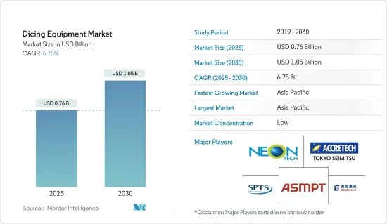
切割设备市场规模预计在 2025 年为 7.6 亿美元,预计到 2030 年将达到 10.5 亿美元,预测期内(2025-2030 年)的复合年增长率为 6.75%。
切割设备对于确保半导体製造的精度起着至关重要的作用。切割机负责从晶圆上切割出单一的晶圆。通常情况下,切割锯会将晶圆上未使用的部分(称为“街道”)切掉,这些部分位于晶圆片之间。这些街道通常有三英里宽,因此它们的狭窄程度比以前更重要,使得切割设备变得更加重要。
关键亮点
- 市场驱动因素包括智慧卡、无线射频辨识(RFID)技术和汽车电源 IC 的需求快速成长。这些因素以及蓬勃发展的家用电子电器市场、不断增加的工厂设置以及小型化和技术迁移的趋势正在鼓励市场供应商增加研发投资。在提高性能的同时注重小型化,这刺激了微电子机械系统 (MEMS) 和 3D 封装等创新。这些领域的持续进步凸显了市场的动态性和适应技术进步的敏捷性。
- 因此,各行业正在开发可以变得更小但仍保持功率等级的半导体。例如,恩智浦半导体公司取得了惊人的成就,在保持功率性能的同时将电晶体的封装尺寸缩小了55%。这项里程碑彰显了业界在不牺牲小封装性能的情况下突破技术界限的努力。
- 此外,Diodes Incorporated 也推出了两款汽车级金属氧化物半导体场场效电晶体(MOSFET),存储DFN2020 封装,占地面积仅 2 mm x 2 mm。这些技术进步进一步加速了半导体和IC封装市场的小型化,增加了对切割设备的需求。这些创新对于满足现代电子设备对小型、高效组件日益增长的需求至关重要。
- 这些进步推动了3D积体电路(3D IC)技术的兴起。该技术在便携式家用电子电器、感测器、微电子机械系统 (MEMS) 和工业产品等空间受限的应用中变得越来越普遍。该技术注重速度、耐用性、低功耗、轻量化设计和增强的记忆体容量,以显着提高整体产品效能。
- 超薄晶圆处理和切割设备製程在各种半导体应用中发挥关键作用,包括 MEMS、复合半导体、LED、扇出型 WLP、CMOS 影像感测器 (CIS) 和利用 TSV 互连的新兴 3D IC。这些製程确保了晶圆的完整性和性能,这对于最终产品的功能和效率至关重要。然而,这些製程技术面临着独特的挑战,例如保持晶圆的稳定性、防止处理过程中的损坏以及确保与现有製造系统的兼容性。
- 削片,其特征是晶片的角落和边缘出现裂缝或碎片,是一个严重的问题。此问题导致製造过程中产量比率降低和成本增加。此外,在切割过程中,切口宽度和切割道宽度(后者相当于切割晶圆的宽度)会增加80-100μm。这会导致切口损失和晶圆浪费。增加切口和切割道宽度不仅会浪费材料,还会影响切割过程的准确性和效率。
- 儘管面临疫情带来的挑战,但部分参与企业仍在对晶圆进行策略性投资。例如,Okmetic Oy 已宣布计划向其芬兰工厂投资数千万欧元,以专注于其核心竞争力。硅晶绝缘体(SOI)晶片。疫情后全球切割设备市场的一个显着趋势是越来越多地采用自动化和先进的控制技术。这一转变预计将提高效率和精度,推动切割设备市场的成长。
切割设备市场趋势
功率元件应用领域可望占据主要市场占有率
- 功率半导体装置用作电力电子电路中的开关和整流器,预计在预测期内将大幅增长。这一快速成长的主要驱动力是全球对行动电话和健康追踪器等可携式电子设备的需求,而有效的电源管理对于延长电池寿命至关重要。此外,对太阳能等替代能源能源的推动以及节能发光二极体(LED) 照明的采用也推动了对这些电源设备的需求。
- 随着应用的发展,对于更小的外形规格、更快的开关频率和更高的电压能力的需求也日益增加。这一演变凸显了功率元件作为产品製造商和加工设备提供者必不可少的积体电路 (IC) 的价值。半导体装置的电源需求不仅在家用电子电器中不断发展,而且在电动车 (EV)、资料中心以及工业和消费者物联网应用等领域也在不断发展。
- 汽车产业,尤其是电动车的兴起,以及可再生能源和家用电子电器等领域,正在推动对最高效切割设备的需求。监管机构也正在采取重要措施。美国运输部部製定了企业平均燃油经济性(CAFE)车辆标准。英国的目标是到2050年实现净零排放,并计划在2035年禁止销售所有污染汽车。德国为自己设定了雄心勃勃的目标,计画在2020年终将温室气体排放减少40%,到2030年减少55%,到2050年减少95%。同时,美国和欧洲政府正在加强排放法规以对抗温室气体。这些共同的努力,加上提高汽车燃油效率的动力,正在增加对电动车以及最终动力设备的需求。
- 现代功率装置受益于雷射切割和先进刀片切割技术等创新,从而实现了更高的精度和效率。例如,ASMPT已经宣布了针对功率半导体市场的解决方案。取得专利的Multi-Beam V-DOE 技术专为切割薄碳化硅 (SiC) 晶片 (<150μm) 而设计。这种改进的光束配置显着增强了晶粒的后期切割性能。
- 作为一项重大的行业进步,英飞凌于 2024 年 9 月宣布推出全球首个用于电力电子的 300 毫米氮化镓 (GaN) 晶圆技术。这项突破性技术有望实现更高的效率、更小的尺寸、更轻的重量和更低的整体晶片成本。
- 随着5G、AI、物联网、边缘运算等技术推动半导体市场的扩张,先进切割设备的需求激增。据SWZD称,北美和欧洲57%的组织已经实施或正在计划实施资讯技术中的物联网趋势。
中国可望占主要市场占有率
- 中国是全球成长最快的半导体市场之一。随着智慧型手机和消费性电子产品的需求激增,许多供应商正在中国建立生产设施。此外,中国政府也倡议吸引国际参与企业设立本地製造工厂。
- 半导体产业协会预测,到2024年,中国半导体产业年收益将达到1,160亿美元,占全球市场占有率。这项预测取决于中国能否在其他国家成长率保持稳定的情况下保持强劲的成长势头。预计的成长凸显了中国在半导体技术方面的战略投资和进步,使中国成为全球市场的重要参与企业。
- 此外,国际半导体设备与材料协会(SEMI)的资料显示,中国晶圆代工产业由跨国公司和国内公司组成,但国内公司将占据主导地位。预计国内企业将在中国价值 240 亿美元的晶圆厂计划中占据很大份额。
- 晶圆製造涉及切割,这是将单个半导体晶片从硅晶圆上分离出来的关键过程。这包括机械锯切、雷射切割和划线等精密切割技术。因此,新兴国家晶圆製造设施的发展预计将产生对晶圆加工中使用的各种切割设备的需求。
- 例如,2024年11月,北京计画投资46亿美元兴建一座12吋晶圆製造厂,由国营企业和基金支持。该计划凸显了中国为加强国内半导体生产所做的持续努力。新工厂由北京燕东微电子(YDME)和中国领先的显示器製造商京东方科技共同投资建设。
切割设备产业概况
市场竞争力是指产业现有参与企业之间的竞争。这种竞争受到品牌识别、竞争策略、透明度和公司集中度等因素的影响。智慧型手机和智慧型手錶等智慧型装置的兴起刺激了对智慧感测器的需求,进而推动了先进半导体市场的发展。
为了追求更大的记忆体和性能而进行的小型化发展也推动了对小型电子封装的需求。因此,薄晶圆在当今小型化电子设备中成为关注的焦点,导致薄晶圆产量激增,随之而来的是加工和切割设备的需求增加。
切割设备市场主要被几家大公司所垄断,例如迪斯可公司、松下公司等。此外,晶圆製造流程中的挑战也减缓了新参与企业进入市场的速度。
主要参与企业包括苏州德尔福雷射、SPTS Technologies Limited(KLA Tencor Corporation)、ASM Laser Separation International (ALSI) BV、Tokyo Seimitsu 和 Neon Tech。
其他福利
- Excel 格式的市场预测 (ME) 表
- 3 个月的分析师支持
目录
第 1 章 简介
- 研究假设和市场定义
- 研究范围
第二章调查方法
第三章执行摘要
第四章 市场洞察
- 市场概况
- 产业吸引力-波特五力分析
- 供应商的议价能力
- 消费者议价能力
- 新进入者的威胁
- 竞争对手之间的竞争
- 替代品的威胁
- 产业价值链分析
- 评估影响市场的宏观经济因素
第五章 市场动态
- 市场驱动因素
- 技术进步和下一代设备的发展
- 市场问题
- 大规模生产挑战
第六章 市场细分
- 透过切割技术
- 刀片划片
- 雷射消熔
- 隐形切割
- 等离子切割
- 按应用
- 逻辑记忆体
- MEMS 设备
- 功率元件
- CMOS影像感测器
- RFID
- 按地区
- 中国
- 台湾
- 韩国
- 北美洲
- 欧洲
- 其他的
第七章 切割设备主要客户列表
第八章 竞争格局
- 公司简介
- Suzhou Delphi Laser Co. Ltd
- SPTS Technologies Limited(KLA Tencor Corporation)
- ASM Laser Separation International(ALSI)BV
- Tokyo Seimitsu Co. Ltd
- Neon Tech Co. Ltd
- Synova SA
- Panasonic Connect Co., Ltd(Panasonic Holdings Corporation)
- Plasma-Therm LLC
- DISCO Corporation
- 3D-Micromac AG
- Veeco Instruments Inc.
- Advanced Dicing Technologies Limited
- Han's Laser Technology Industry Group Co., Ltd
- EO Technics Co., Ltd.
第九章投资分析
第十章:投资分析市场的未来
The Dicing Equipment Market size is estimated at USD 0.76 billion in 2025, and is expected to reach USD 1.05 billion by 2030, at a CAGR of 6.75% during the forecast period (2025-2030).
Dicing equipment plays a pivotal role in ensuring precision during semiconductor manufacturing. The equipment is responsible for cutting individual dice from a wafer. Typically, a dicing saw slices through an unused section of the wafer, referred to as the 'street,' which is located between the dice. These streets generally measure three miles in width, and their narrowing heightens the significance of the dicing equipment.
Key Highlights
- Key drivers propelling the growth of the studied market encompass surging demands for smart cards, Radio Frequency Identification (RFID) technology, and automotive power ICs. Alongside a flourishing consumer electronics market, an increase in factory establishments, and a trend towards miniaturization and technology migration, these factors have urged market vendors to amplify their research and development investments. This emphasis on downsizing while boosting performance has catalyzed innovations such as micro-electro-mechanical systems (MEMS) and 3D packaging. The ongoing advancements in these domains underscore the market's dynamic nature and its agility in adapting to technological progress.
- As a result, industry players are developing semiconductors that sustain power levels even with size reductions. For instance, NXP Semiconductors achieved a remarkable 55% reduction in package size for its transistors, all while maintaining power performance. This milestone highlights the industry's dedication to pushing technical boundaries, ensuring that compact packages do not sacrifice performance.
- Furthermore, Diodes Incorporated unveiled two automotive-compliant metal-oxide-semiconductor field-effect transistors (MOSFET) housed in a DFN2020 package, occupying a mere 2 mm by 2 mm footprint. Such strides accentuate the upward trajectory of the miniaturized semiconductor and IC packaging markets, subsequently amplifying the demand for dicing equipment. These innovations are paramount, addressing the escalating need for compact and efficient components in contemporary electronic devices.
- These advancements have catalyzed the ascent of three-dimensional integrated circuits (3D ICs) technology. This technology is becoming increasingly popular in space-constrained applications, spanning portable consumer electronics, sensors, Micro-Electro-Mechanical Systems (MEMS), and industrial products. It significantly boosts overall product performance, emphasizing speed, durability, low power consumption, lightweight design, and enhanced memory capacity.
- Ultra-thin wafer handling and dicing equipment processes play a crucial role in various semiconductor applications, including MEMS, compound semiconductors, LEDs, fan-out WLP, CMOS image sensors (CIS), and the emerging 3D ICs utilizing TSV interconnects. These processes ensure the integrity and performance of the wafers, which are essential for the functionality and efficiency of the end products. Nevertheless, these processing technologies face specific challenges, such as maintaining wafer stability, preventing damage during handling, and ensuring compatibility with existing manufacturing systems.
- Chipping, characterized by the cracking or chipping of the corners and edges of chips, poses a significant challenge. This issue can lead to reduced yield and increased costs in the manufacturing process. Furthermore, during dicing, the kerf width and the street width (the latter corresponding to the width of the diced wafer) increase by 80 to 100 μm. Consequently, this results in a kerf loss, leading to wastage of the wafers. The increased kerf width and street width not only waste material but also impact the precision and efficiency of the dicing process.
- Despite the challenges posed by the pandemic, certain players are making strategic investments in wafers. For example, Okmetic Oy announced plans to invest tens of millions of euros in its Finland facility, focusing on its core competency: Silicon-On-Insulator (SOI) wafers. Post-pandemic, a prominent trend in the global dicing equipment market is the rising adoption of automation and advanced control technologies. This shift is anticipated to enhance efficiency and precision, subsequently driving the dicing equipment market growth.
Dicing Equipment Market Trends
Power Devices Application Segment is Expected to Hold Significant Market Share
- Power semiconductor devices, utilized as switches or rectifiers in power electronic circuits, are poised for substantial growth during the forecast period. This surge is primarily driven by the global appetite for cell phones and portable electronics, such as health trackers, where effective power management is crucial for extending battery life. Additionally, the demand for these power devices is bolstered by the push for alternative energy sources like solar power and the adoption of energy-efficient Light Emitting Diode (LED) lighting.
- As applications evolve, there's a growing demand for smaller form factors, faster-switching frequencies, and higher voltage capabilities. This evolution underscores the value of power devices as essential integrated circuits (ICs) for product manufacturers and processing equipment providers. Beyond consumer electronics, sectors like electric vehicles (EVs), data centers, and both industrial and consumer IoT applications are witnessing evolving power requirements for semiconductor devices.
- The automotive industry, particularly with the rise of electric vehicles, alongside sectors like renewable energy and consumer electronics, is driving a heightened demand for top-tier, efficient dicing equipment. Regulatory bodies are taking significant steps: The US Department of Transportation has established Corporate Average Fuel Economy (CAFE) vehicle standards. The UK aims for net-zero emissions by 2050 and plans to ban the sale of all polluting vehicles by 2035. Germany has set ambitious targets, seeking a 40% reduction in greenhouse gas emissions by the end of 2020, 55% by 2030, and up to 95% by 2050. Concurrently, US and European governments are tightening emission limits to combat the greenhouse effect. These concerted efforts, alongside a push for enhanced vehicle fuel economy, are amplifying the demand for electric vehicles and, in turn, power devices.
- Modern power devices are benefiting from innovations like laser dicing and advanced blade dicing techniques, which offer enhanced precision and efficiency. For example, ASMPT has introduced a solution for the power semiconductor market. Their patented multi-beam V-DOE technology is designed for dicing through thin Silicon Carbide (SiC) wafers (less than 150 µm). This modified beam configuration notably strengthens the die post-cutting.
- In a significant industry advancement, Infineon unveiled the world's first 300mm Gallium Nitride (GaN) wafer technology for power electronics in September 2024. This breakthrough promises enhanced efficiency, reduced size and weight, and a lower overall cost for chips.
- As technologies like 5G, AI, IoT, and edge computing propel the semiconductor market's expansion, the demand for sophisticated dicing equipment has surged. According to SWZD, 57 percent of organizations in North America and Europe have either implemented or plan to implement IoT trend in information technology.
China is Expected to Hold Significant Market Share
- China stands out as one of the fastest-growing semiconductor markets globally. The surging demand for smartphones and consumer electronics is prompting numerous vendors to establish production facilities in the nation. Further, the Chinese government's initiatives are attracting international players to set up local production units.
- The Semiconductor Industry Association forecasts that by 2024, China's semiconductor industry will generate an annual revenue of USD 116 billion, capturing over 17.4% of the global market share. This forecast depends on China maintaining its strong growth momentum, assuming other countries' growth rates remain stable. The anticipated growth underscores China's strategic investments and advancements in semiconductor technology, positioning it as a significant player in the global market.
- Further, Semiconductor Equipment and Materials International's (SEMI) data indicates that while China's foundry industry comprises both multinational and domestic vendors, domestic companies are poised to dominate. Out of the USD 24 billion fab projects in China, domestic firms are expected to command a significant share.
- Wafer fabrication includes dicing, a critical process where individual semiconductor chips are separated from a silicon wafer. This involves precise cutting techniques such as mechanical sawing, laser cutting, and scribing. Thus, the development of new wafer fabrication facilities in the country is expected to generate demand for various dicing equipment used in wafer processing.
- For instance, in November 2024, Beijing, supported by state-owned enterprises and funds, plans to invest USD 4.6 billion in a 12-inch wafer fabrication facility. This initiative highlights China's ongoing efforts to strengthen its domestic semiconductor production. The new facility involves Beijing Yandong Microelectronics (YDME) and BOE Technology, China's leading display manufacturer.
Dicing Equipment Industry Overview
Competitive rivalry in the market refers to the competition among established players in the industry. This competition is influenced by factors such as brand identity, competitive strategies, transparency levels, and the concentration ratio of firms. The rise of smart devices, including smartphones and smartwatches, has spurred the demand for smart sensors, consequently boosting the market for advanced semiconductors.
Factors like the trend towards miniaturization, aiming for enhanced memory and performance in smaller sizes, have spurred demand for compact electronic packages. As a result, thin wafers have gained prominence in today's miniaturized electronics landscape, leading to a surge in thin wafer production and a corresponding demand for processing and dicing equipment.
The dicing equipment market is dominated by a handful of major players, including Disco Corporation and Panasonic Corporation, among others. Additionally, challenges in thin wafer manufacturing processes have slowed the entry of new players into the market.
Some of the major players in the market are Suzhou Delphi Laser Co. Ltd, SPTS Technologies Limited (KLA Tencor Corporation), ASM Laser Separation International (ALSI) BV, Tokyo Seimitsu Co. Ltd, and Neon Tech Co. Ltd.
Additional Benefits:
- The market estimate (ME) sheet in Excel format
- 3 months of analyst support
TABLE OF CONTENTS
1 INTRODUCTION
- 1.1 Study Assumptions and Market Definition
- 1.2 Scope of the Study
2 RESEARCH METHODOLOGY
3 EXECUTIVE SUMMARY
4 MARKET INSIGHTS
- 4.1 Market Overview
- 4.2 Industry Attractiveness - Porter's Five Forces Analysis
- 4.2.1 Bargaining Power of Suppliers
- 4.2.2 Bargaining Power of Consumers
- 4.2.3 Threat of New Entrants
- 4.2.4 Intensity of Competitive Rivalry
- 4.2.5 Threat of Substitutes
- 4.3 Industry Value Chain Analysis
- 4.4 Assessment of Macroeconomic Factors on the Market
5 MARKET DYNAMICS
- 5.1 Market Drivers
- 5.1.1 Technological Advancements, and Evolution of Next Generation Devices
- 5.2 Market Challenges
- 5.2.1 Mass Manufacturing Challenges
6 MARKET SEGMENTATION
- 6.1 By Dicing Technology
- 6.1.1 Blade Dicing
- 6.1.2 Laser Ablation
- 6.1.3 Stealth Dicing
- 6.1.4 Plasma Dicing
- 6.2 By Application
- 6.2.1 Logic & Memory
- 6.2.2 MEMS Devices
- 6.2.3 Power Devices
- 6.2.4 CMOS Image Sensor
- 6.2.5 RFID
- 6.3 By Geography
- 6.3.1 China
- 6.3.2 Taiwan
- 6.3.3 South Korea
- 6.3.4 North America
- 6.3.5 Europe
- 6.3.6 Rest of the World
7 POTENTIAL LIST OF KEY CUSTOMERS FOR DICING EQUIPMENT
8 COMPETITIVE LANDSCAPE
- 8.1 Company Profiles
- 8.1.1 Suzhou Delphi Laser Co. Ltd
- 8.1.2 SPTS Technologies Limited (KLA Tencor Corporation)
- 8.1.3 ASM Laser Separation International (ALSI) BV
- 8.1.4 Tokyo Seimitsu Co. Ltd
- 8.1.5 Neon Tech Co. Ltd
- 8.1.6 Synova SA
- 8.1.7 Panasonic Connect Co., Ltd (Panasonic Holdings Corporation)
- 8.1.8 Plasma-Therm LLC
- 8.1.9 DISCO Corporation
- 8.1.10 3D-Micromac AG
- 8.1.11 Veeco Instruments Inc.
- 8.1.12 Advanced Dicing Technologies Limited
- 8.1.13 Han's Laser Technology Industry Group Co., Ltd
- 8.1.14 EO Technics Co., Ltd.

