


 |
市场调查报告书
商品编码
1844674
奈米辐射感测器:市场份额分析、行业趋势、统计数据和成长预测(2025-2030)Nano Radiation Sensors - Market Share Analysis, Industry Trends & Statistics, Growth Forecasts (2025 - 2030) |
||||||
※ 本网页内容可能与最新版本有所差异。详细情况请与我们联繫。
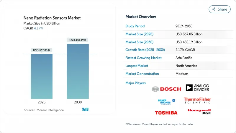
预计到 2025 年奈米辐射感测器市场规模将达到 3,670.5 亿美元,复合年增长率为 4.17%,到 2030 年将达到 4,501.9 亿美元。
成长反映了家用电子电器、航太和汽车系统的持续小型化,以及核能发电厂退役和太空探索方面严格的安全法规。钙钛矿半导体材料的最新突破使检测器的占地面积足够小,可以整合智慧型手机和可穿戴贴片,消除了长期存在的尺寸和功率障碍。政府奖励策略,从英国核能退役管理局提供的 3000 万英镑一揽子计划到为 ADI 公司提供的 1.05 亿美元 CHIPS 法案拨款,正在缩短商业化週期并加速供应扩张。立方卫星的激增,特别是在大学和新兴企业任务中的激增,增加了超轻型感测器的可寻址容量,同时医疗剂量测定和汽车安全子系统的需求也在增加。虽然製造复杂性和产量比率下降仍然是最显着的限制因素,但能够解决材料稳定性问题同时保持成本控制的公司将获得直接的竞争优势。
全球奈米辐射感测器市场趋势与洞察
各行业的裁员趋势
消费性电子产品和汽车平台的持续小型化推动了辐射感测器模组在晶圆级的整合。夏普展示了一款25 x 20 x 2.5毫米的模组,功耗仅7.5毫瓦,使智慧型手机中的辐射追踪实用化成为可能。 5奈米和3奈米製程节点的平行发展使逻辑电路和检测电路共用通用晶粒,从而降低了目标商标产品製造商的物料清单成本。在汽车领域,微型感测器现在可以安装在现有的电控系统内,因此无需改变驾驶室设计即可支援高级驾驶辅助系统(ADAS)。随着物联网架构的日益普及,分散式奈米辐射感测器可以以五年前无法企及的节点级成本部署在工厂和医院。
政府奈米技术资金和标准
有针对性的公共计画确保了长期需求,同时协调了认证。美国商务部向ADI公司拨款1.05亿美元,用于其三家国内工厂的现代化改造。英国核能退役管理局已承诺投入3,000万英镑用于感测器研发,以支持老旧核子反应炉的安全退役。同时,欧盟委员会的「地平线欧洲」平台正将资源投入永续辐射防护技术。 ISO和IEEE工作小组目前正在起草统一的奈米感测器测试通讯协定,以缩短合规週期并实现跨境采购。
製造复杂性和产量比率损失
先进检测器架构所需的10奈米以下製程的缺陷率高于主流逻辑晶片,导致一些代工厂的一次通过产量比率低于60%。供应链衝击,例如为光刻光罩基板提供高纯度二氧化硅的Spruce Pine石英矿的暂时关闭,透过限制关键材料供应,加剧了成本压力。晶圆厂营运商不得不采用更严格的颗粒控制和先进的计量技术,从而在短期内推高了每片晶圆的营运成本。
細項分析
固体检测器利用CMOS相容性将感测元件直接整合到混合讯号晶片上,到2024年将占奈米辐射感测器市场收入的58%。这种架构在医学成像和卫星设备中很受欢迎,因为它可以降低功耗并简化基板布局。闪烁单元虽然市占率较小,但由于钙钛矿奈米晶体的突破,其光输出已超过100,000 MeV-1,因此正受惠于6.5%的复合年增长率。将固体读出与奈米晶体闪烁体结合的混合设计现已实现低于400 ps的响应速度,同时保持了晶圆级加工的经济性。
第二代固体平台采用奈米等离子体增强层,在不增加占地面积的情况下将光子收集效率提高了三倍。随着钙钛矿涂层的成熟,製造商正在尝试将高Z闪烁体单晶片整合到硅光电二极体上,旨在打造用于内视镜手术的单晶片伽马摄影机。这一发展表明固体方法和闪烁方法之间的界限正在模糊,为整个奈米辐射感测器产业创造了新的收益来源。
到2024年,硅材料将维持46%的收入贡献,透过提供可靠的供应和广泛的代工支持,支撑当前主流应用的奈米辐射感测器市场规模。良好的生产学习曲线使平均售价保持可预测性,这对于致力于十年产品週期的一级汽车供应商至关重要。钙钛矿检测器的复合年增长率为8.2%,得益于能够实现软式电路板捲对辊涂的溶液处理技术,从而拓展了可穿戴健康监测器和无人机平台的应用机会。
将硅基ASIC与薄钙钛矿吸收层结合的复合堆迭,能够在单一封装内侦测软X射线和低能量伽玛光子,从而改善无损检测的频谱成像。以锰错合为特征的无铅组合物可提供超过80%的光致发光量子产率,在不牺牲检测效率的情况下实现环境升级。这些混合堆迭代表着曲折点,材料选择决策将不再受供应链约束,而是取决于具体应用。
奈米辐射感测器市场按类型(闪烁检测器、固体检测器)、材料(硅基半导体、无机晶体(GAGG、LSO、Csi)等)、应用(汽车、消费性电子等)、技术(间接闪烁 - CMOS 等)、探测辐射类型、外形尺寸和地区细分。市场预测以美元计算。
区域分析
北美的领先地位将在2024年达到35%的份额,这得益于持续的国防采购和耗资数十亿美元对93座运作中的核子反应炉进行现代化升级。 ADI公司正在根据《晶片法案》(CHIPS Act)将其在马萨诸塞州和奥勒冈州的晶圆产量增加两倍,以确保军用级检测器的长期供应。赛默飞世尔科技正在扩大其在美国的64个製造地网络,以加强医疗保健、工业无损检测和国防安全保障项目的国内供应,同时提供人工智能驱动的监控和预测分析,以减少美国两座压水式反应炉的计划外停机时间。
受中国智慧型手机相容辐射晶片成功推广的推动,亚太地区将以5.9%的复合年增长率位居榜首。日本凭藉夏普的超薄感测器模组和日本原子能机构(JAEA)用于沸水式反应炉维修的硅伽马射线检测器,保持了其在核领域的专业优势。韩国NEXTSat-2卫星上的LEO-DOS有效载荷将检验其自主研发的低轨道剂量抗辐射设计,并向东南亚新兴航太经济体展示可出口的潜力。
在欧洲,安全退役171吉瓦的核能发电厂,这些核电厂将于2050年前逐步淘汰,这将在短期内导致分散式感测器阵列的需求达到高峰。英国将拨款3000万英镑津贴一个产学研联盟,开发自主机器人监测器的原型。一家德国一级汽车供应商正在考虑将辐射感测技术纳入ADAS控制单元,以确保电子设备免受单粒子故障的影响;法国电力公司(EDF)正在使用奈米感测器升级堆芯通量测绘技术,以将核电站许可证的有效期延长至60年或更长时间。芬兰于韦斯屈莱大学开发了一种手持式多用途检测器,它结合了中子、伽马射线和β射线,为芬兰各地的初期应变人员套件提供支援。
其他福利:
- Excel 格式的市场预测 (ME) 表
- 3个月的分析师支持
目录
第一章 引言
- 研究假设和市场定义
- 调查范围
第二章调查方法
第三章执行摘要
第四章 市场状况
- 市场概况
- 市场驱动因素
- 整个产业都朝着小型化发展
- 政府奈米技术资助和标准化
- 高精度医疗剂量计的需求不断增加
- 核能退役和安全法规
- 立方卫星和小型卫星采用奈米感测器
- 使用柔性钙钛矿闪烁体的可穿戴剂量测定
- 市场限制
- 製造复杂性和产量比率损失
- 奈米製造生产线的资本成本高昂
- 原始设备製造商之间缺乏整合标准
- 钙钛矿/有机材料的稳定性问题
- 价值/供应链分析
- 监管状况
- 技术展望
- 关键绩效指标(KPI)
- 波特五力分析
- 新进入者的威胁
- 买方的议价能力
- 供应商的议价能力
- 替代品的威胁
- 竞争对手之间的竞争强度
第五章市场规模及成长预测
- 按类型
- 闪烁检测器
- 固体检测器
- 按材质
- 硅基半导体
- 无机晶体(GAGG、LSO、CsI)
- 钙钛矿半导体(含铅和无铅)
- 有机/聚合物闪烁体
- 按用途
- 车
- 消费性电子产品
- 卫生保健
- 产业
- 石油和天然气
- 发电
- 其他用途
- 依技术
- 直接转换(光子计数)
- 间接闪烁-CMOS
- 柔性/穿戴面板
- 抗辐射SoC和SiPM
- 根据侦测到的辐射类型
- 阿尔法
- β射线
- 伽玛射线/X射线
- 中子
- 外形规格
- 晶片级
- 模组
- 控制板
- 穿戴式贴片
- 按地区
- 北美洲
- 美国
- 加拿大
- 墨西哥
- 南美洲
- 巴西
- 阿根廷
- 其他南美
- 欧洲
- 英国
- 德国
- 法国
- 义大利
- 俄罗斯
- 西班牙
- 其他欧洲国家
- 亚太地区
- 中国
- 日本
- 印度
- 韩国
- 其他亚太地区
- 中东和非洲
- 中东
- 阿拉伯聯合大公国
- 沙乌地阿拉伯
- 土耳其
- 其他中东地区
- 非洲
- 南非
- 埃及
- 其他非洲国家
- 北美洲
第六章 竞争态势
- 市场集中度
- 策略倡议
- 市占率分析
- 公司简介
- Analog Devices Inc.
- Robert Bosch GmbH
- Nihon Kessho Kogaku Co. Ltd.
- Thermo Fisher Scientific Inc.
- Baker Hughes Co.
- Honeywell International Inc.(RAE Systems)
- First Sensor AG(TE Connectivity)
- Hamamatsu Photonics KK
- Toshiba Corporation
- Mirion Technologies Inc.
- Fortive Corporation
- PerkinElmer Inc.(Revvity)
- Radiation Monitoring Devices Inc.
- Texas Instruments Inc.
- Lockheed Martin Corp.
- OMRON Corporation
- Space Micro Inc.
- Analogic Corporation
- Canon Medical Systems Corp.
- Siemens Healthineers AG
- GE Healthcare Technologies Inc.
- BAE Systems plc
- Hitachi Ltd.
- STMicroelectronics NV
第七章 市场机会与未来展望
The nano radiation sensors market stood at USD 367.05 billion in 2025 and is forecast to register a 4.17% CAGR, reaching USD 450.19 billion by 2030.
Growth reflects consistent miniaturization across consumer electronics, aerospace, and automotive systems, paired with stringent safety rules in nuclear decommissioning and space exploration. Recent breakthroughs in perovskite semiconductor materials now allow detector footprints small enough for smartphone integration and wearable patches, removing long-standing size and power barriers. Government stimulus ranging from the GBP 30 million package under the UK Nuclear Decommissioning Authority to the USD 105 million CHIPS Act grant for Analog Devices shortens commercialization cycles and accelerates supply expansion. CubeSat proliferation, particularly in university and startup missions, compounds the addressable volume for ultra-light sensors, while parallel demand arises from healthcare dosimetry and automotive safety subsystems. Manufacturing complexity and yield losses remain the most significant constraints; however, firms that resolve material-stability issues while maintaining cost control gain an immediate competitive edge.
Global Nano Radiation Sensors Market Trends and Insights
Miniaturization trend across industries
Relentless downsizing in consumer electronics and automotive platforms pushes radiation sensor modules toward wafer-level integration. Sharp demonstrated a 25 X 20 X 2.5 mm module drawing only 7.5 mW, making smartphone-based radiation tracking practical. Parallel progress in 5 nm and 3 nm process nodes allows logic and detection circuitry to share a common die, lowering bill-of-materials costs for original-equipment manufacturers. In automobiles, compact sensors now fit inside existing electronic control units, supporting Advanced Driver Assistance Systems without altering cabin design. As IoT architectures spread, distributed nano radiation sensors can be deployed in factories and hospitals at node-level costs that were unattainable five years ago.
Government nanotech funding and standards
Targeted public programs guarantee long-term demand while harmonizing certification. The U.S. Department of Commerce earmarked USD 105 million for Analog Devices to modernize three domestic fabs, explicitly citing commercial and defense radiation detection as priority outputs. The UK Nuclear Decommissioning Authority injected GBP 30 million into sensor R & D to support safe dismantling of legacy reactors. In parallel, the European Commission's Horizon Europe platform directs resources toward sustainable radiation-protection technology. ISO and IEEE working groups now draft unified nano sensor test protocols that cut compliance cycles and enable cross-border procurement.
Manufacturing complexity and yield losses
Sub-10 nm features needed for latest detector architectures experience higher defect rates than mainstream logic chips, depressing first-pass yields below 60% at several foundries. Supply-chain shocks-such as the temporary shutdown of Spruce Pine's quartz mine that feeds high-purity silica into photolithography mask blanks-amplify cost pressures by constricting vital materials. Fab operators must adopt tighter particulate controls and advanced metrology, driving up per-wafer operating expenses in the short run.
Other drivers and restraints analyzed in the detailed report include:
- Growing demand for high-precision healthcare dosimetry
- Nuclear decommissioning and safety regulations
- Stability issues of perovskite / organic materials
For complete list of drivers and restraints, kindly check the Table Of Contents.
Segment Analysis
Solid-state detectors captured 58% of 2024 revenue within the nano radiation sensors market, leveraging CMOS compatibility to embed sensing elements directly onto mixed-signal chips. This architecture trims power budgets and simplifies board layouts, attributes valued in medical imaging consoles and satellite payloads. Scintillation units, though smaller in share, benefit from 6.5% CAGR prospects tied to perovskite nanocrystal breakthroughs delivering light yields above 100,000 photons MeV-1. Hybrid designs now merge solid-state readout with nanocrystal scintillators, achieving sub-400 ps response while retaining wafer-level processing economies.
Second-generation solid-state platforms adopt nano-plasmonic enhancement layers that triple photon-collection efficiency without expanding footprint. As perovskite coatings mature, manufacturers experiment with monolithic integration of high-Z scintillators atop silicon photodiodes, pointing toward single-chip gamma cameras for endoscopic surgery. The evolution indicates that categorical boundaries between solid-state and scintillation approaches will blur, generating new revenue pools throughout the nano radiation sensors industry.
Silicon maintained 46% contribution to 2024 revenue, offering reliable supply and extensive foundry support that underpins the current nano radiation sensors market size for mainstream applications. Production learning curves keep average selling prices predictable, a trait essential for automotive Tier-1 suppliers committing to decade-long product cycles. Perovskite detectors, at 8.2% CAGR, benefit from solution processing that allows roll-to-roll coating of flexible substrates, widening addressable opportunities in wearable health monitors and drone platforms.
Composite stacks merging silicon ASICs with thin perovskite absorber layers allow detection of soft X-ray and low-energy gamma photons in a single envelope, improving multispectral imaging for nondestructive testing. Lead-free compositions featuring manganese complexes reach photoluminescence quantum yields above 80%, providing an environmental upgrade without sacrificing detection efficiency. These hybrid stacks signal an inflection point where material-choice decisions become application-specific rather than supply-chain constrained.
Nano Radiation Sensors Market Segmented by Type (Scintillation Detectors, Solid-State Detectors), Material (Silicon-Based Semiconductors, Inorganic Crystals (GAGG, LSO, Csi) and More), Application (Automotive, Consumer Electronics and More), Technology, Indirect Scintillation-CMOS and More), Detection Radiation Type, Form Factor and Geography. The Market Forecasts are Provided in Terms of Value (USD).
Geography Analysis
North American leadership, with 35% 2024 share, is anchored by continuous defense procurement and multi-billion-dollar modernization across 93 operating nuclear reactors. Analog Devices is tripling wafer starts in Massachusetts and Oregon under the CHIPS Act, securing long-run availability of military-grade detectors. Thermo Fisher's enlarged US network of 64 manufacturing sites reinforces domestic supply for healthcare, industrial NDT, and homeland-security programs, while AI-augmented monitoring at two US pressurized-water reactors cuts unscheduled outage hours through predictive analytics.
APAC shows the fastest 5.9% CAGR forecast, underpinned by China's successful scaling of smartphone-compatible radiation chips, which broaden public-safety adoption. Japan maintains domain expertise via Sharp's ultra-thin sensor module and JAEA's silicon gamma-ray detectors qualified for boiling-water reactor retrofits. South Korea's LEO-DOS payload on NEXTSat-2 validates homegrown radiation-hard designs for low-Earth-orbit dosimetry, signalling export-ready competence for emerging space economies in Southeast Asia.
Europe prioritizes safe dismantling of 171 GW of nuclear capacity set for phase-out before 2050, creating near-term demand peaks for distributed sensor arrays. The UK's GBP 30 million research grant seeds university-industry consortia to prototype autonomous robotic monitors. Germany's automotive Tier-1 suppliers explore integrating radiation sensing into ADAS control units to certify electronics against single-event upsets, while France's EDF upgrades core flux mapping with nano sensors to extend plant licenses beyond 60 years. Finland's University of Jyvaskyla produced a handheld multi-purpose detector that merges neutron, gamma, and beta channels, supporting first-responder toolkits across the continent.
- Analog Devices Inc.
- Robert Bosch GmbH
- Nihon Kessho Kogaku Co. Ltd.
- Thermo Fisher Scientific Inc.
- Baker Hughes Co.
- Honeywell International Inc. (RAE Systems)
- First Sensor AG (TE Connectivity)
- Hamamatsu Photonics KK
- Toshiba Corporation
- Mirion Technologies Inc.
- Fortive Corporation
- PerkinElmer Inc. (Revvity)
- Radiation Monitoring Devices Inc.
- Texas Instruments Inc.
- Lockheed Martin Corp.
- OMRON Corporation
- Space Micro Inc.
- Analogic Corporation
- Canon Medical Systems Corp.
- Siemens Healthineers AG
- GE Healthcare Technologies Inc.
- BAE Systems plc
- Hitachi Ltd.
- STMicroelectronics N.V.
Additional Benefits:
- The market estimate (ME) sheet in Excel format
- 3 months of analyst support
TABLE OF CONTENTS
1 INTRODUCTION
- 1.1 Study Assumptions and Market Definition
- 1.2 Scope of the Study
2 RESEARCH METHODOLOGY
3 EXECUTIVE SUMMARY
4 MARKET LANDSCAPE
- 4.1 Market Overview
- 4.2 Market Drivers
- 4.2.1 Miniaturization trend across industries
- 4.2.2 Government nanotech funding and standards
- 4.2.3 Growing demand for high-precision healthcare dosimetry
- 4.2.4 Nuclear decommissioning and safety regulations
- 4.2.5 CubeSat and small-sat adoption of nano-sensors
- 4.2.6 Flexible perovskite scintillators enable wearable dosimetry
- 4.3 Market Restraints
- 4.3.1 Manufacturing complexity and yield losses
- 4.3.2 High capital cost of nano-fabrication lines
- 4.3.3 Lack of integration standards across OEMs
- 4.3.4 Stability issues of perovskite / organic materials
- 4.4 Value / Supply-Chain Analysis
- 4.5 Regulatory Landscape
- 4.6 Technological Outlook
- 4.7 Key Performance Indicators (KPIs)
- 4.8 Porter's Five Forces Analysis
- 4.8.1 Threat of New Entrants
- 4.8.2 Bargaining Power of Buyers
- 4.8.3 Bargaining Power of Suppliers
- 4.8.4 Threat of Substitutes
- 4.8.5 Intensity of Competitive Rivalry
5 MARKET SIZE AND GROWTH FORECASTS (VALUE)
- 5.1 By Type
- 5.1.1 Scintillation Detectors
- 5.1.2 Solid-state Detectors
- 5.2 By Material
- 5.2.1 Silicon-based Semiconductors
- 5.2.2 Inorganic Crystals (GAGG, LSO, CsI)
- 5.2.3 Perovskite Semiconductors (Lead and Lead-free)
- 5.2.4 Organic / Polymer Scintillators
- 5.3 By Application
- 5.3.1 Automotive
- 5.3.2 Consumer Electronics
- 5.3.3 Healthcare
- 5.3.4 Industrial
- 5.3.5 Oil and Gas
- 5.3.6 Power Generation
- 5.3.7 Other Applications
- 5.4 By Technology
- 5.4.1 Direct-conversion (Photon-counting)
- 5.4.2 Indirect Scintillation-CMOS
- 5.4.3 Flexible / Wearable Panels
- 5.4.4 Radiation-hardened SoC and SiPM
- 5.5 By Detection Radiation Type
- 5.5.1 Alpha
- 5.5.2 Beta
- 5.5.3 Gamma / X-ray
- 5.5.4 Neutron
- 5.6 By Form Factor
- 5.6.1 Chip-scale
- 5.6.2 Module
- 5.6.3 Panel
- 5.6.4 Wearable Patch
- 5.7 By Geography
- 5.7.1 North America
- 5.7.1.1 United States
- 5.7.1.2 Canada
- 5.7.1.3 Mexico
- 5.7.2 South America
- 5.7.2.1 Brazil
- 5.7.2.2 Argentina
- 5.7.2.3 Rest of South America
- 5.7.3 Europe
- 5.7.3.1 United Kingdom
- 5.7.3.2 Germany
- 5.7.3.3 France
- 5.7.3.4 Italy
- 5.7.3.5 Russia
- 5.7.3.6 Spain
- 5.7.3.7 Rest of Europe
- 5.7.4 Asia-Pacific
- 5.7.4.1 China
- 5.7.4.2 Japan
- 5.7.4.3 India
- 5.7.4.4 South Korea
- 5.7.4.5 Rest of Asia-Pacific
- 5.7.5 Middle East and Africa
- 5.7.5.1 Middle East
- 5.7.5.1.1 United Arab Emirates
- 5.7.5.1.2 Saudi Arabia
- 5.7.5.1.3 Turkey
- 5.7.5.1.4 Rest of Middle East
- 5.7.5.2 Africa
- 5.7.5.2.1 South Africa
- 5.7.5.2.2 Egypt
- 5.7.5.2.3 Rest of Africa
- 5.7.1 North America
6 COMPETITIVE LANDSCAPE
- 6.1 Market Concentration
- 6.2 Strategic Moves
- 6.3 Market Share Analysis
- 6.4 Company Profiles {(includes Global level Overview, Market level overview, Core Segments, Financials as available, Strategic Information, Market Rank/Share for key companies, Products and Services, and Recent Developments)}
- 6.4.1 Analog Devices Inc.
- 6.4.2 Robert Bosch GmbH
- 6.4.3 Nihon Kessho Kogaku Co. Ltd.
- 6.4.4 Thermo Fisher Scientific Inc.
- 6.4.5 Baker Hughes Co.
- 6.4.6 Honeywell International Inc. (RAE Systems)
- 6.4.7 First Sensor AG (TE Connectivity)
- 6.4.8 Hamamatsu Photonics KK
- 6.4.9 Toshiba Corporation
- 6.4.10 Mirion Technologies Inc.
- 6.4.11 Fortive Corporation
- 6.4.12 PerkinElmer Inc. (Revvity)
- 6.4.13 Radiation Monitoring Devices Inc.
- 6.4.14 Texas Instruments Inc.
- 6.4.15 Lockheed Martin Corp.
- 6.4.16 OMRON Corporation
- 6.4.17 Space Micro Inc.
- 6.4.18 Analogic Corporation
- 6.4.19 Canon Medical Systems Corp.
- 6.4.20 Siemens Healthineers AG
- 6.4.21 GE Healthcare Technologies Inc.
- 6.4.22 BAE Systems plc
- 6.4.23 Hitachi Ltd.
- 6.4.24 STMicroelectronics N.V.
7 MARKET OPPORTUNITIES AND FUTURE OUTLOOK
- 7.1 White-space and Unmet-need Assessment


