


 |
市场调查报告书
商品编码
1850025
氮化镓半导体装置:市场份额分析、产业趋势、统计数据和成长预测(2025-2030 年)GaN Semiconductor Devices - Market Share Analysis, Industry Trends & Statistics, Growth Forecasts (2025 - 2030) |
||||||
※ 本网页内容可能与最新版本有所差异。详细情况请与我们联繫。
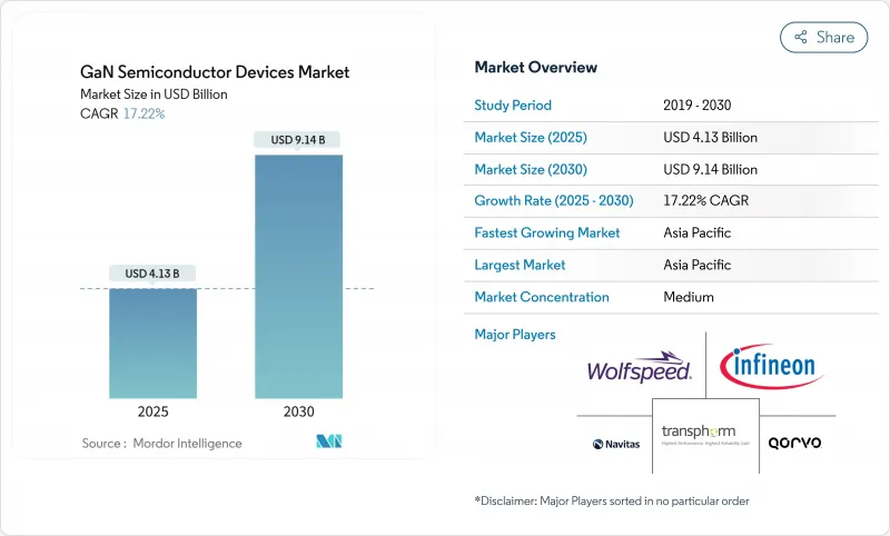
预计到 2025 年,氮化镓半导体装置市场规模将达到 41.3 亿美元,到 2030 年将达到 91.4 亿美元。
这一增长反映了氮化镓(GaN)相较于传统硅材料所固有的更高效率、更快开关速度和更优异的散热性能。同时,日益严格的全球能源效率法规促使资料中心营运商和工业OEM厂商寻求基于GaN的转换级,以降低损耗和冷却成本。企业投资也印证了这个趋势,英飞凌和瑞萨等现有企业透过收购扩大GaN产能,而日本和欧盟的区域性激励措施也加速了能够处理6吋和8吋晶圆的待开发区的建设。
全球氮化镓半导体装置市场趋势及洞察
中国OEM厂商的蓝图推动了65-240W USB-C PD GaN充电器的普及。
中国消费电子品牌迅速推动了超紧凑型USB(USB)充电器的普及。 2024年推出的新款充电器功率高达240W,但体积却比同等硅基充电器缩小了40%,零售价格降低了35%。 Anker的GaN Prime系列充电器功率密度超过1.8W/cm³,可在口袋大小的机壳内实现笔记型电脑和行动电话的多重通讯协定充电。成本的下降推动了其在亚太和北美市场的普及,进而带动了氮化镓半导体装置市场的销售成长。
亚洲和印度的 5G 大规模 MIMO大型基地台部署需要 200W 以上的 GaN-on-SiC 功率放大器
2024年,中国、印度和日本的行动电话电信商在3.5GHz及以上频宽部署了超过15,000个采用GaN-on-SiC功率放大器的广域基地台。这项转变使功耗降低了25%,覆盖范围扩大了18%,为日本大型通讯业者每年节省了1,800万美元的营运成本。这些经济效益巩固了GaN功率放大器的应用,并拓展了氮化镓半导体装置市场的商机。
由于200mm GaN-on-Si外延晶片供应有限,供应链出现瓶颈。
预计到2024年,能够生产200毫米氮化镓外延晶圆的优质供应商将不到10家。产量比率比硅基标准低15-20%,限制了产能并维持了高昂的价格。一家欧洲一级汽车供应商的生产延误了六个月,迫使其建立价值2800万欧元(3020万美元)的战略库存缓衝。瓶颈正在影响氮化镓半导体装置市场的近期销售。
细分市场分析
预计到2024年,氮化镓半导体装置市场中功率半导体部分将占据55.2%的份额,并在2030年之前保持在19.1%的份额。资料中心营运商透过升级到效率高达98.2%的氮化镓伺服器电源,每个设施节省了230万美元。射频元件也紧跟其后,因为5G大规模MIMO基础设施和国防雷达的需求持续强劲。
成熟标誌着一个战略性的分水岭。像英飞凌这样的硅製造商扩展了其车规级氮化镓MOSFET产品线,而像Wolfspeed这样的射频专家则利用碳化硅上氮化镓的热余量,开发出频率高于3.5 GHz的大型基地台。整合式功率级供应商不再局限于分立元件销售,而是获得了更高的利润。因此,氮化镓半导体装置市场经历了整合和垂直一体化,从而增强了规模优势。
到2024年,高电子移动性电晶体将占总收入的57.2%,而单晶片功率积体电路将以31.1%的复合年增长率超越所有其他类别。一家中国智慧型手机OEM厂商透过单一GaN积体电路取代分立开关,将充电器物料成本降低了18%,零件数量减少了45%,推动了销售成长。
随着整合化改善电磁相容性并减少寄生效应,氮化镓半导体元件市场正朝着系统级封装设计发展,而模组製造商则迎合高功率安装的需求,二极体在辅助整流领域的销售依然强劲。
与消费性电子、资料中心和48V工业用电标准相符的100-650V电压区间,预计到2024年将维持70.3%的市场占有率。同时,以800V驱动架构为驱动的650V+频宽,将以42.2%的复合年增长率成长。某高阶电动车品牌采用900V氮化镓(GaN)平台,将10-80%的充电时间缩短至28分钟,并相比碳化硅(SiC)充电器减轻了3.2公斤的重量。
这项转变将推动新的分离和测试标准,对纯供应商构成挑战,但氮化镓半导体装置市场将奖励那些能够检验650 V 以上可靠性的供应商,释放利润丰厚的汽车价值池。
GaN半导体装置市场按元件类型(功率半导体、其他)、组件(电晶体、其他)、额定电压(小于100V、其他)、晶圆尺寸(2英吋、其他)、基板技术(GaN-On-SiC、其他)、封装(表面黏着技术、其他)、用户产业(汽车、北美地区、其他国家)。
区域分析
亚太地区将占2024年销售额的38.2%,成长最快,复合年增长率达29.1%。中国丰富的镓资源和国家补贴使Innoscience得以营运全球最大的8吋GaN-on-Si晶圆厂,成本比同业低35%。一家韩国大型家电製造商和一家日本大型汽车製造商成为其大量生产的核心客户,并维持了需求与产能扩张的良性循环。
北美持续是创新的温床。一项价值3500万美元的联邦晶片创新计划(CHIPS)拨款帮助GlobalFoundries公司扩大了其位于佛蒙特州的氮化镓(GaN)产能。一家国防承包商部署了一款基于氮化镓的相位阵列,在将侦测范围提高42%的同时,功耗降低了18%,这充分展现了氮化镓半导体装置市场在关键任务应用方面的优势。
在欧洲,高端汽车和工业应用场景成为优先考虑的领域。剑桥氮化镓装置公司(Cambridge GaN Devices)筹集了3,050万欧元(约3,310万美元)用于扩张,反映出投资者对欧洲高功率细分市场的看好。一家德国大型原始设备製造商(OEM)实现了97.8%的充电器效率,并减少了30%的组件,符合欧盟绿色设计指令的要求。拉丁美洲和中东及非洲目前市场份额较小,但随着能源价格和基础设施建设的融合,这些地区在电讯和智慧城市计划中展现出令人瞩目的成长潜力。
其他福利:
- Excel格式的市场预测(ME)表
- 3个月的分析师支持
目录
第一章 引言
- 研究假设和市场定义
- 调查范围
第二章调查方法
第三章执行摘要
第四章 市场情势
- 市场概览
- 市场驱动因素
- 中国OEM厂商蓝图图推动65-240W USB-C PD GaN充电器的普及
- 亚洲和印度的 5G 大规模 MIMO大型基地台部署需要 200W 以上的 GaN-on-SiC 功率放大器
- 向 800V 电动车平台的迁移推动了双向 GaN OBC 和 DC-DC 转换器的应用。
- 在重量关键型电动飞机和电动垂直起降飞行器动力传动系统中选择氮化镓转换器
- 低卫星群星座卫星过渡到氮化镓Ku/ Ka波段功率放大器
- 日本和欧盟晶圆厂奖励加速氮化镓产能扩张
- 市场限制
- 200毫米GaN-on-Si晶圆供应链瓶颈
- 门可靠性挑战 >175℃ 汽车 0 级认证
- 新兴市场中低于 3.5GHz 宏功率放大器的成本Delta与 LDMOS 的比较
- E型GaN QFN/CSP封装的测试/封装生态系分散
- 价值链分析
- 监理与技术展望
- 波特五力分析
- 供应商的议价能力
- 买方的议价能力
- 新进入者的威胁
- 替代品的威胁
- 竞争对手之间的竞争
- 影响市场的宏观经济因素
第五章 市场规模与成长预测
- 依设备类型
- 功率半导体
- 射频半导体
- 光学半导体
- 按组件
- 电晶体(HEMT/FET)
- 二极体(肖特基二极体、PiN二极体)
- 整流器
- 功率积体电路(单晶片、多晶片)
- 模组(半桥、全桥)
- 按额定电压
- 低于100伏
- 100~650V
- 超过650伏
- 按晶圆尺寸
- 2英吋
- 4吋
- 6吋或以上(包括8吋导轮)
- 透过基板技术
- GaN-on-SiC
- GaN-on-Si
- 蓝宝石基板上的氮化镓
- 体氮化镓
- 650~1200V
- 1200伏特或以上
- 透过包装
- 表面黏着技术(QFN、DFN)
- 通孔(TO-220、TO-247)
- 晶片级封装(CSP)
- 裸晶
- 按最终用户行业划分
- 汽车与出行
- 电动车
- 充电基础设施
- 消费性电子产品
- 智慧型手机快速充电器
- 笔记型电脑和平板电脑充电器
- 游戏主机和虚拟现实
- 通讯和资料通讯
- 5G基地台
- 资料中心电源
- 工业和能源
- 太阳能逆变器
- 马达驱动
- 电源单元(SMPS)
- 航太与国防
- 雷达系统
- 电子战
- 卫星有效载荷卫星有效载荷
- 药品
- 磁振造影和电脑断层扫描
- 可携式医疗设备
- 汽车与出行
- 按地区
- 北美洲
- 美国
- 加拿大
- 墨西哥
- 南美洲
- 巴西
- 阿根廷
- 其他南美洲
- 欧洲
- 德国
- 英国
- 法国
- 义大利
- 西班牙
- 其他欧洲地区
- 亚太地区
- 中国
- 日本
- 韩国
- 印度
- 台湾
- 亚太其他地区
- 中东和非洲
- 中东
- 沙乌地阿拉伯
- 阿拉伯聯合大公国
- 土耳其
- 其他中东地区
- 非洲
- 南非
- 其他非洲地区
- 北美洲
第六章 竞争情势
- 市场集中度
- 策略趋势
- 市占率分析
- 公司简介
- Efficient Power Conversion Corporation
- Navitas Semiconductor
- Transphorm Inc.
- Innoscience Technology Co., Ltd.
- MACOM Technology Solutions Holdings, Inc.
- Tagore Technology Inc.
- VisIC Technologies Ltd.
- Cambridge GaN Devices Ltd.
- NexGen Power Systems, Inc.
- Qromis, Inc.
- EPC Space LLC
- Analog Devices, Inc.
- Power Integrations, Inc.
- Ommic SAS
- Wolfspeed GaN Solutions
- Ampleon Netherlands BV
- Integra Technologies, Inc.
- RFHIC Corporation
- Sumitomo Electric Device Innovations Inc.
- Infineon Technologies AG
- STMicroelectronics NV
- Qorvo Inc.
第七章 市场机会与未来展望
The gallium nitride semiconductor devices market size stood at USD 4.13 billion in 2025 and is forecast to touch USD 9.14 billion by 2030, reflecting a robust 17.22% CAGR.
The surge mirrors GaN's intrinsic ability to deliver higher efficiency, faster switching, and superior thermal performance when compared with legacy silicon. Market momentum was reinforced in 2024 and early 2025 by three concurrent shifts: 800 V electric-vehicle powertrains, large-scale 5G rollouts that require high-power radio-frequency amplifiers, and consumer demand for ultra-compact USB-C chargers exceeding 100 W. At the same time, global energy-efficiency regulations tightened, pushing data-center operators and industrial OEMs toward GaN-based conversion stages that cut losses and shrink cooling overhead. Corporate investment underscored the trend as Infineon, Renesas, and other incumbents expanded GaN capacity through acquisitions, while regional incentives in Japan and the European Union accelerated green-field fabs geared to 6-inch and 8-inch wafers.
Global GaN Semiconductor Devices Market Trends and Insights
Proliferation of 65-240 W USB-C PD GaN Chargers Led by Chinese OEM Road-maps
Chinese consumer-electronics brands propelled a rapid shift toward ultra-compact universal serial bus power-delivery chargers. Models released in 2024 delivered up to 240 W while shrinking volume by 40% relative to silicon equivalents and lowering retail prices by 35%. Anker's GaN Prime line exceeded 1.8 W/cm3 power density, enabling multiprotocol charging for laptops and phones within pocket-sized enclosures. Cost-downs stimulated mainstream uptake across Asia-Pacific and North America, lifting unit volumes that ripple across the gallium nitride semiconductor devices market.
5G Massive-MIMO Macro-Cell Roll-outs Requiring >200 W GaN-on-SiC PAs in Asia and India
Mobile network operators in China, India, and Japan deployed more than 15,000 macro base stations in 2024 using GaN-on-SiC power amplifiers above 3.5 GHz. The switch trimmed power consumption by 25% and stretched coverage by 18%, translating into USD 18 million annual operating expense savings for one leading Japanese carrier. Such economics cement GaN PA design wins and expand addressable revenue across the gallium nitride semiconductor devices market.
Limited 200 mm GaN-on-Si Epi Wafer Supply Chain Bottlenecks
Fewer than 10 qualified suppliers produced 200 mm GaN epitaxial wafers in 2024. Yields sat 15-20% below silicon benchmarks, constraining throughput and sustaining premium pricing. A European Tier-1 automotive supplier recorded a six-month production delay that forced strategic inventory buffers worth EUR 28 million (USD 30.2 million). Bottlenecks weigh on near-term volumes within the gallium nitride semiconductor devices market.
Other drivers and restraints analyzed in the detailed report include:
- Shift to 800 V EV Platforms Driving Bidirectional GaN OBC and DC-DC Adoption
- Weight-Critical More-Electric Aircraft and eVTOL Powertrains Selecting GaN Converters
- Gate Reliability Challenges >175 °C for Automotive Grade-0 Qualification
For complete list of drivers and restraints, kindly check the Table Of Contents.
Segment Analysis
The power-semiconductor slice of the gallium nitride semiconductor devices market held 55.2% share in 2024 and is projected to compound at 19.1% to 2030. Data-center operators saved USD 2.3 million per facility by upgrading to GaN server power supplies that reached 98.2% efficiency. RF devices followed as 5G massive-MIMO infrastructure and defense radar sustained premium demand.
Maturity signaled a strategic fork. Silicon incumbents such as Infineon expanded automotive-grade GaN MOSFET lines, while RF specialists like Wolfspeed leveraged GaN-on-SiC thermal headroom for >3.5 GHz macro cells. Integrated power-stage providers captured a higher margin by moving beyond discrete sales. The gallium nitride semiconductor devices market, therefore, experiences both consolidation and vertical integration, reinforcing scale advantages.
High-electron-mobility transistors occupied 57.2% revenue in 2024, yet monolithic power ICs outpaced all other categories at 31.1% CAGR. A Chinese smartphone OEM cut the charger bill-of-materials by 18% by replacing discrete switches with a single GaN IC, shrinking part count by 45% and catalyzing volume ramps.
Integration improves electromagnetic compatibility and trims parasitics, benefits that explain why the gallium nitride semiconductor devices market is tilting toward system-in-package designs. Module suppliers address high-power installations, while diode sales remain steady in auxiliary rectification roles.
The 100-650 V corridor kept a 70.3% share in 2024 as it aligns with consumer, data-center, and 48 V industrial rails. Meanwhile, the >650 V band races ahead at 42.2% CAGR, fueled by 800 V propulsion architectures. One premium EV brand slashed 10-80% charge time to 28 minutes using 900 V GaN stages and cut charger mass by 3.2 kg versus SiC.
This transition prompts new isolation and test standards, challenging pure-play suppliers. Nevertheless, the gallium nitride semiconductor devices market rewards those able to validate reliability beyond 650 V, unlocking lucrative automotive value pools.
The GaN Semiconductor Devices Market is Segmented by Device Type (Power Semiconductors, and More), Component (Transistors, and More), Voltage Rating (< 100 V, and More), Wafer Size (2-Inch, and More), Substrate Technology (GaN-On-SiC, and More), Packaging (Surface-Mount, and More), End-User Industry (Automotive and Mobility, and More), and Geography (North America, South America, Europe, Asia-Pacific, and Middle East and Africa).
Geography Analysis
Asia-Pacific commanded 38.2% of 2024 sales and remained the fastest riser at 29.1% CAGR. China's access to gallium, plus state subsidies, allowed Innoscience to operate the world's largest 8-inch GaN-on-Si plant at costs 35% below peers. South Korea's consumer-electronics titans and Japan's automotive majors seeded high-volume anchor customers, sustaining a virtuous cycle of demand and capacity growth.
North America stayed an innovation hotbed. Federal CHIPS grants of USD 35 million helped GlobalFoundries broaden GaN capacity in Vermont. Defense contractors deployed GaN-based phased-array radars that boosted detection range by 42% while trimming power by 18%, showcasing mission-critical gains that flow into the gallium nitride semiconductor devices market.
Europe prioritized premium automotive and industrial use cases. Cambridge GaN Devices raised EUR 30.5 million (USD 33.1 million) for expansion, reflecting investor belief in high-power European niches. A leading German OEM realized 97.8% charger efficiency and 30% component reduction, aligning with EU eco-design directives. Latin America, the Middle East, and Africa presently hold modest shares yet demonstrate promising uptake in telecom and smart-city projects as energy prices and infrastructure buildouts converge.
- Efficient Power Conversion Corporation
- Navitas Semiconductor
- Transphorm Inc.
- Innoscience Technology Co., Ltd.
- MACOM Technology Solutions Holdings, Inc.
- Tagore Technology Inc.
- VisIC Technologies Ltd.
- Cambridge GaN Devices Ltd.
- NexGen Power Systems, Inc.
- Qromis, Inc.
- EPC Space LLC
- Analog Devices, Inc.
- Power Integrations, Inc.
- Ommic SAS
- Wolfspeed GaN Solutions
- Ampleon Netherlands B.V.
- Integra Technologies, Inc.
- RFHIC Corporation
- Sumitomo Electric Device Innovations Inc.
- Infineon Technologies AG
- STMicroelectronics N.V.
- Qorvo Inc.
Additional Benefits:
- The market estimate (ME) sheet in Excel format
- 3 months of analyst support
TABLE OF CONTENTS
1 INTRODUCTION
- 1.1 Study Assumptions and Market Definition
- 1.2 Scope of the Study
2 RESEARCH METHODOLOGY
3 EXECUTIVE SUMMARY
4 MARKET LANDSCAPE
- 4.1 Market Overview
- 4.2 Market Drivers
- 4.2.1 Proliferation of 65-240 W USB-C PD GaN Chargers Led by Chinese OEM Road-maps
- 4.2.2 5G Massive-MIMO Macro-Cell Roll-outs Requiring >200 W GaN-on-SiC PAs in Asia and India
- 4.2.3 Shift to 800 V EV Platforms Driving Bidirectional GaN OBC and DC-DC Adoption
- 4.2.4 Weight-Critical More-Electric Aircraft and eVTOL Powertrains Selecting GaN Converters
- 4.2.5 LEO Constellation Satellites Migrating to GaN Ku/Ka-Band SSPAs
- 4.2.6 Japanese and EU Fab Incentives Accelerating GaN Capacity Expansion
- 4.3 Market Restraints
- 4.3.1 Limited 200 mm GaN-on-Si Epi Wafer Supply Chain Bottlenecks
- 4.3.2 Gate Reliability Challenges >175 °C for Automotive Grade-0 Qualification
- 4.3.3 Cost Delta vs. LDMOS in Sub-3.5 GHz Macro PAs in Emerging Markets
- 4.3.4 Fragmented Test/Packaging Ecosystem for E-mode GaN QFN/CSP Packages
- 4.4 Value Chain Analysis
- 4.5 Regulatory and Technological Outlook
- 4.6 Porter's Five Forces Analysis
- 4.6.1 Bargaining Power of Suppliers
- 4.6.2 Bargaining Power of Buyers
- 4.6.3 Threat of New Entrants
- 4.6.4 Threat of Substitutes
- 4.6.5 Intensity of Competitive Rivalry
- 4.7 Impact of Macroeconomic Factors on the market
5 MARKET SIZE AND GROWTH FORECASTS (VALUE)
- 5.1 By Device Type
- 5.1.1 Power Semiconductors
- 5.1.2 RF Semiconductors
- 5.1.3 Opto-Semiconductors
- 5.2 By Component
- 5.2.1 Transistors (HEMT/FET)
- 5.2.2 Diodes (Schottky, PiN)
- 5.2.3 Rectifiers
- 5.2.4 Power ICs (Monolithic, Multi-chip)
- 5.2.5 Modules (Half-bridge, Full-bridge)
- 5.3 By Voltage Rating
- 5.3.1 < 100 V
- 5.3.2 100 - 650 V
- 5.3.3 > 650 V
- 5.4 By Wafer Size
- 5.4.1 2-inch
- 5.4.2 4-inch
- 5.4.3 6-inch and Above (incl. 8-inch Pilot)
- 5.5 By Substrate Technology
- 5.5.1 GaN-on-SiC
- 5.5.2 GaN-on-Si
- 5.5.3 GaN-on-Sapphire
- 5.5.4 Bulk GaN
- 5.5.5 650 - 1200 V
- 5.5.6 > 1200 V
- 5.6 By Packaging
- 5.6.1 Surface-Mount (QFN, DFN)
- 5.6.2 Through-Hole (TO-220, TO-247)
- 5.6.3 Chip-Scale Package (CSP)
- 5.6.4 Bare Die
- 5.7 By End-User Industry
- 5.7.1 Automotive and Mobility
- 5.7.1.1 Electric Vehicles
- 5.7.1.2 Charging Infrastructure
- 5.7.2 Consumer Electronics
- 5.7.2.1 Smartphone Fast Chargers
- 5.7.2.2 Laptop and Tablet Chargers
- 5.7.2.3 Gaming Consoles and VR
- 5.7.3 Telecom and Datacom
- 5.7.3.1 5G Base Stations
- 5.7.3.2 Data Center Power
- 5.7.4 Industrial and Energy
- 5.7.4.1 Solar Inverters
- 5.7.4.2 Motor Drives
- 5.7.4.3 Power Supply Units (SMPS)
- 5.7.5 Aerospace and Defense
- 5.7.5.1 Radar Systems
- 5.7.5.2 Electronic Warfare
- 5.7.5.3 Satellite Payloads
- 5.7.6 Medical
- 5.7.6.1 MRI and CT
- 5.7.6.2 Portable Medical Devices
- 5.7.1 Automotive and Mobility
- 5.8 By Geography
- 5.8.1 North America
- 5.8.1.1 United States
- 5.8.1.2 Canada
- 5.8.1.3 Mexico
- 5.8.2 South America
- 5.8.2.1 Brazil
- 5.8.2.2 Argentina
- 5.8.2.3 Rest of South America
- 5.8.3 Europe
- 5.8.3.1 Germany
- 5.8.3.2 United Kingdom
- 5.8.3.3 France
- 5.8.3.4 Italy
- 5.8.3.5 Spain
- 5.8.3.6 Rest of Europe
- 5.8.4 Asia-Pacific
- 5.8.4.1 China
- 5.8.4.2 Japan
- 5.8.4.3 South Korea
- 5.8.4.4 India
- 5.8.4.5 Taiwan
- 5.8.4.6 Rest of Asia-Pacific
- 5.8.5 Middle East and Africa
- 5.8.5.1 Middle East
- 5.8.5.1.1 Saudi Arabia
- 5.8.5.1.2 United Arab Emirates
- 5.8.5.1.3 Turkey
- 5.8.5.1.4 Rest of Middle East
- 5.8.5.2 Africa
- 5.8.5.2.1 South Africa
- 5.8.5.2.2 Rest of Africa
- 5.8.1 North America
6 COMPETITIVE LANDSCAPE
- 6.1 Market Concentration
- 6.2 Strategic Moves
- 6.3 Market Share Analysis
- 6.4 Company Profiles (includes Global level Overview, Market level overview, Core Segments, Financials as available, Strategic Information, Market Rank/Share for key companies, Products and Services, Recent Developments)
- 6.4.1 Efficient Power Conversion Corporation
- 6.4.2 Navitas Semiconductor
- 6.4.3 Transphorm Inc.
- 6.4.4 Innoscience Technology Co., Ltd.
- 6.4.5 MACOM Technology Solutions Holdings, Inc.
- 6.4.6 Tagore Technology Inc.
- 6.4.7 VisIC Technologies Ltd.
- 6.4.8 Cambridge GaN Devices Ltd.
- 6.4.9 NexGen Power Systems, Inc.
- 6.4.10 Qromis, Inc.
- 6.4.11 EPC Space LLC
- 6.4.12 Analog Devices, Inc.
- 6.4.13 Power Integrations, Inc.
- 6.4.14 Ommic SAS
- 6.4.15 Wolfspeed GaN Solutions
- 6.4.16 Ampleon Netherlands B.V.
- 6.4.17 Integra Technologies, Inc.
- 6.4.18 RFHIC Corporation
- 6.4.19 Sumitomo Electric Device Innovations Inc.
- 6.4.20 Infineon Technologies AG
- 6.4.21 STMicroelectronics N.V.
- 6.4.22 Qorvo Inc.
7 MARKET OPPORTUNITIES AND FUTURE OUTLOOK
- 7.1 White-Space and Unmet-Need Assessment
 氮化镓雷达系统市场:按类型、组件、频宽、组件范围和应用划分-2026年至2032年全球预测
 高频氮化镓半导体市场分析及预测(至2035年):依类型、产品类型、服务、技术、应用、材料类型、装置、部署类型、最终用户和功能划分氮化镓半导体装置市场分析及预测(至2035年):按类型、产品类型、技术、组件、应用、材料类型、装置、最终用户、功能和解决方案划分
 2026-2034年全球氮化镓半导体装置市场规模、份额、趋势和成长分析报告
 GaN HEMT晶圆:全球市场份额和排名、总收入和需求预测(2026-2032年)
 2026年全球氮化镓半导体装置市场报告
 氮化镓半导体市场-全球产业规模、份额、趋势、机会及预测(依产品、组件、最终用户、地区及竞争格局划分),2021-2031年
 2026-2030年全球氮化镓(GaN)半导体装置市场GaN HEMT代工市场按应用、电压等级、装置类型、终端用户产业、晶圆尺寸、製程模式、基板材料、销售管道和服务类型划分,全球预测,2026-2032年GaN雷达技术市场按类型、频段、组件和应用划分,全球预测(2026-2032年)