


 |
市场调查报告书
商品编码
1850979
原子层沉积(ALD)设备:市场占有率分析、产业趋势、统计数据和成长预测(2025-2030 年)Atomic Layer Deposition Equipment - Market Share Analysis, Industry Trends & Statistics, Growth Forecasts (2025 - 2030) |
||||||
※ 本网页内容可能与最新版本有所差异。详细情况请与我们联繫。
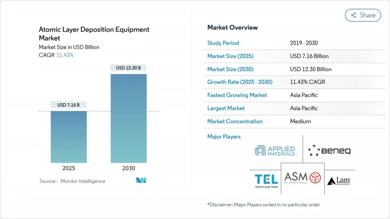
预计到 2025 年,原子层沉积 (ALD) 设备市场规模将达到 71.6 亿美元,到 2030 年将达到 123 亿美元,年复合成长率为 11.43%。
这项扩张主要受先进逻辑和3D储存节点製程强度不断提高、环栅(GAA)电晶体的普及以及固态电池和微型LED生产线需求激增的推动。亚太地区大规模晶圆厂的建设,加上美国和欧盟的政策奖励,正在扩大单晶圆、批量和太空平台的需求。设备製造商透过引入高通量反应器、提供低电阻率金属薄膜(例如钌和钼)以及整合即时前驱体使用分析来获取价值。同时,前驱体短缺、PFAS法规以及降低单晶圆成本的需求,正促使工具供应商和晶片製造商更加关注製程整合和供应链韧性。
全球原子层沉积(ALD)设备市场趋势及洞察
亚洲3D NAND和DRAM製程节点快速缩小
商用3D NAND元件已超过200层,需要沉积数十层高长宽比的介电层和金属层,沉积精度需达到亚埃级。韩国和中国的主要记忆体製造商对能够将100:1长宽比结构的厚度偏差控制在1%以下的热原子层沉积(ALD)反应器的订单激增。记忆体价格在2024年至2025年间回升,带动工厂运转率恢復,儘管面临出口限制的不利因素,设备需求依然强劲。 2024年,中国晶圆厂购入了全球40%的晶圆製造设备,导致ALD前驱体产能出现区域性供不应求。能够兼顾批量经济性和高介电常数均匀性的供应商获得了最多的设备替换订单。
全方位闸极设计及向高k金属闸极逻辑的过渡
GAA架构将栅极电极移至奈米带上,从而增加了每个装置的共形高介电常数/金属层数量。台积电的2nm平台计画于2025年下半年量产,该平台简化了数百道ALD製程步骤,与3nm节点相比,功耗降低了25-30%,同时确保了阈值电压调节器。钼和钌ALD已在某些互连层取代了钨和铜,使线路电阻降低了35%,并简化了CMP製程。市场需求偏向具有源内计量功能的单晶圆设备,该设备可在每个循环后检验薄膜厚度。能够以每小时200瓦或更高的吞吐量提供2埃或更小的薄膜厚度重复性的供应商处于行业领先地位。
前驱金属稀少与成本波动
钌和铱的供应链仍集中在两个生产国,这意味着晶圆厂到2024年将面临超过40%的价格波动。一家领先的逻辑晶圆厂由于钌短缺,将其3nm产推出推迟了三个月,并增加了一套前驱体回收装置,导致设备资本支出增加了15%。锌烷基辅助钴原子层沉积(ALD)的研究已将薄片电阻降低至15µΩcm,但其电迁移寿命仍低于钌。在替代化学製程成熟之前,铂族金属(PGM)的价格将限制积极的成本削减蓝图。
细分市场分析
到2024年,热感原子层沉积(ALD)将占据ALD设备市场最大的份额,达到55.2%。单晶圆热感反应器对于高深长宽比记忆体蚀刻停止层至关重要,其配方灵活性支援频繁的前驱体更换。然而,太空ALD以17.1%的复合年增长率脱颖而出,成为2030年成长最快的技术。一家OLED面板製造商检验了大气压力空间ALD封装,使其产能提高了四倍,并满足了严格的阻隔性能指标。因此,每平方公尺成本下降了28%,新订单也转向了线上空间ALD设备。等离子体增强ALD扩大了其在软性电子产品的应用范围,使其能够在低于100°C的温度下进行沉积,这对于塑胶基板至关重要。供应商也推出了卷轴式版本,推动ALD技术应用于食品和太阳能组件的阻隔薄膜领域。
受显示器和太阳能电池工厂需求的推动,用于太空原子层沉积(ALD)的设备市场规模预计将比其他任何领域更快成长。另一方面,支援原子层蚀刻(ALE)的平台已成为一个新的细分市场。透过将沉积和蚀刻整合到单一框架中,可以缩短232层NAND快闪记忆体的阶梯蚀刻製程的等待时间。这些发展使收入来源不再局限于核心半导体领域。
丛集系统将占2024年营收的65.2%,这得益于3奈米以下逻辑生产线配方的弹性。近期升级结合了先进的前驱体蒸汽输送和机器学习故障检测技术,使週期时间缩短了25%,晶圆间均匀性提高了40%。这些生产力的提升有助于单晶圆设备保持了其市场份额优势。
然而,随着记忆体和类比电路製造厂寻求降低单片晶圆成本,批式反应器正在重新兴起。新型热壁反应器设计可同时处理 100 片晶圆,并将温度控制在 ±1°C 以内。一家韩国记忆体製造商将其介质衬垫製程从集群式原子层沉积 (ALD) 过渡到批量式 ALD 后,成本降低了 30%。因此,批量製程的收入以 14.3% 的复合年增长率成长,超过了整体市场的成长速度。
ALD(原子层沉积)设备市场报告按设备类型(热 ALD、其他)、反应器配置(群集、独立批次)、基板尺寸(小于 200 毫米、其他)、薄膜化学(氧化物、氮化物、氧氮化物、其他)、应用(半导体逻辑、记忆体、其他)和地区(北美、南美、欧洲、亚太、中东和非洲)进行细分。
区域分析
预计亚太地区在2024年将维持41.8%的营收份额,并在2030年前以17.3%的复合年增长率成长。台湾、韩国和中国大陆生产了全球80%以上的逻辑和储存晶圆,从而集中了对晶圆製造设备的需求。儘管受到出口限制,但得益于470亿美元的国家基金支持,仅中国大陆在2024年仍将采购全球40%的晶圆製造设备。该地区还拥有全球最高的微型LED产能,并日益广泛地采用太空原子层沉积(ALD)技术。
北美则位居第二,这主要得益于CHIPS和科学法案的激励措施。亚利桑那州、俄亥俄州和德克萨斯州的新建晶圆厂累计数十亿美元用于GAA试点生产线和先进晶片封装的ALD设备。美国企业将在2023年投入1,075亿美元用于研发和资本支出,进而提振国内需求。
欧洲的份额虽小,但成长迅速。欧洲晶片计画已筹集430亿欧元(490.9亿美元),其中包括37亿欧元(42.2亿美元)用于五条采用原子层沉积(ALD)技术进行先进封装堆迭原型开发的试点生产线。巴西、以色列和阿联酋的新活动拓展了客户群,主要体现在针对电力电子和可再生能源储存领域的研究。
其他福利:
- Excel格式的市场预测(ME)表
- 3个月的分析师支持
目录
第一章 引言
- 研究假设和市场定义
- 调查范围
第二章调查方法
第三章执行摘要
第四章 市场情势
- 市场概览
- 市场驱动因素
- 亚洲3D NAND和DRAM製程节点快速缩小
- 向环栅(GAA)和高介电常数金属闸极逻辑的过渡
- 快速采用迷你/微型LED背板
- 电动汽车电池用固体电解质被覆剂的需求
- 用于提高生物相容性的医用植入奈米涂层
- 政府资助的试点生产线投资(欧盟晶片法案、晶片计画、科学法案)
- 市场限制
- 前驱体金属(Ru、Ir、Co)的稀少性与成本波动性
- 吞吐量限制和大批量晶圆代工厂目标
- OLED封装空间CVD领域的竞争
- 氟化血浆製品的严格环境、健康与安全 (EHS) 法规
- 价值链分析
- 监理与技术展望
- 波特五力模型
- 供应商的议价能力
- 买方的议价能力
- 新进入者的威胁
- 替代品的威胁
- 竞争对手之间的竞争
- 宏观经济因素如何影响市场
第五章 市场规模与成长预测
- 透过装置
- 热感原子层沉积(批量)
- 等离子体增强原子层沉积(PEALD)
- 空间ALD
- 卷对卷/片对片原子层沉积
- 原子层蚀刻 (ALE) 相容工具
- 按反应器配置
- 丛集(单晶圆)
- 独立批次
- 按基板尺寸
- 200毫米或更小
- 300 mm
- 450毫米或更长的导线
- 透过薄膜化学
- 氧化膜
- 氮化物和氧氮化物薄膜
- 金属薄膜(Co、Ru、Ti、Al、Cu)
- 氟化物和硫化物薄膜
- 透过使用
- 半导体逻辑和记忆体
- 先进封装和异构集成
- 功率和光电子(SiC、GaN、LED)
- 能源装置(锂离子电池、固体燃料电池)
- 生物医学和植入表面功能化
- 汽车感测器和ADAS
- 按地区
- 北美洲
- 美国
- 加拿大
- 墨西哥
- 南美洲
- 巴西
- 阿根廷
- 其他南美洲
- 欧洲
- 德国
- 英国
- 法国
- 义大利
- 西班牙
- 俄罗斯
- 其他欧洲地区
- 亚太地区
- 中国
- 日本
- 印度
- 韩国
- 东南亚
- 亚太其他地区
- 中东和非洲
- 中东
- 沙乌地阿拉伯
- 阿拉伯聯合大公国
- 土耳其
- 其他中东地区
- 非洲
- 南非
- 奈及利亚
- 其他非洲地区
- 北美洲
第六章 竞争情势
- 市场集中度
- 策略性倡议和合资分析
- 市占率分析
- 公司简介
- ASM International NV
- Applied Materials Inc.
- Tokyo Electron Limited
- Lam Research Corporation
- Veeco Instruments Inc.
- Oxford Instruments plc
- Beneq Oy
- Picosun Oy
- Entegris Inc.
- Kurt J. Lesker Company
- Hitachi High-Tech Corporation
- Ulvac Inc.
- Aixtron SE
- SENTECH Instruments GmbH
- CVD Equipment Corporation
- Forge Nano Inc.
- ALD NanoSolutions Inc.
- Lotus Applied Technology
- LPE SpA
- SVT Associates
- Arradiance LLC
- Beneq R2R(Service Business)
第七章 市场机会与未来展望
The atomic layer deposition equipment market size stood at USD 7.16 billion in 2025 and is forecast to reach USD 12.30 billion by 2030, reflecting an 11.43% CAGR.
This expansion has been propelled by rising process intensity at advanced logic and 3-D memory nodes, adoption of gate-all-around (GAA) transistors, and fast-growing demand from solid-state battery and micro-LED lines. Asia-Pacific's large wafer-fab build-out, coupled with policy incentives in the United States and European Union, has enlarged the buyer base for single-wafer, batch, and spatial platforms. Equipment makers are capturing value by introducing high-throughput reactors, offering lower-resistance metal films such as ruthenium and molybdenum, and embedding real-time precursor-utilization analytics. Meanwhile, precursor scarcity, PFAS regulation, and the need to trim cost-per-wafer keep process integration and supply-chain resilience at centre stage for tool vendors and chipmakers alike.
Global Atomic Layer Deposition Equipment Market Trends and Insights
Surging 3-D NAND and DRAM Node Shrink in Asia
Layer counts already surpassed 200 in commercial 3-D NAND devices, requiring dozens of high-aspect-ratio dielectric and metal layers deposited with sub-Angstrom precision. Leading memory makers in South Korea and China ramped orders for thermal ALD reactors that can maintain thickness variation below 1% across structures with 100:1 aspect ratios. Memory price recovery in 2024-2025 restored fab utilization, raising tool demand even amid export-control headwinds. Chinese fabs purchased 40% of global wafer-fab equipment in 2024, creating a regional undersupply of ALD precursor capacity. Vendors able to couple batch economics with high-k dielectric uniformity won most replacement awards.
Transition to Gate-All-Around and High-k Metal Gate Logic
GAA architectures move the gate electrode around the entire nanoribbon, multiplying the number of conformal high-k/metal layers per device. TSMC's 2 nm platform, slated for 2H 2025 mass production, integrates hundreds of ALD steps to secure threshold-voltage control while shaving 25-30% power versus 3 nm nodes. Molybdenum and ruthenium ALD replaced tungsten and copper in several interconnect levels, trimming line resistance by 35% and simplifying CMP. Demand has skewed toward single-wafer tools with in-source metrology that validates film thickness after every cycle. Suppliers capable of delivering sub-2 A thickness repeatability at >200 Wph throughput are best positioned.
Scarcity and Cost Volatility of Precursor Metals
Ruthenium and iridium supply chains remained concentrated in two producing nations, exposing fabs to price swings above 40% in 2024. One leading-edge logic fab deferred a 3 nm ramp by three months owing to Ru shortages, adding precursor-recycling skids that raised tool CAPEX by 15%. Research into zinc-alkyl-assisted cobalt ALD cut sheet resistance to 15 µΩ cm but still trails Ru in electromigration life. Until alternative chemistries mature, the price of PGMs will cap aggressive cost-down roadmaps.
Other drivers and restraints analyzed in the detailed report include:
- Rapid Adoption of Mini/Micro-LED Backplanes
- EV Battery Solid-State Electrolyte Coatings Demand
- Throughput Limitations vs. High-Volume Foundry Targets
For complete list of drivers and restraints, kindly check the Table Of Contents.
Segment Analysis
Thermal ALD captured the largest slice of the atomic layer deposition equipment market at 55.2% in 2024. Single-wafer thermal reactors proved indispensable for high-aspect-ratio memory etch-stop layers, with recipe flexibility supporting frequent precursor swaps. However, spatial ALD's 17.1% CAGR makes it the standout gainer through 2030. A top OLED panel maker validated atmospheric spatial ALD encapsulation that quadrupled throughput and met stringent barrier metrics. The resulting cost per square meter fell by 28%, steering fresh orders toward in-line spatial tools. Plasma-enhanced ALD widened its appeal for flexible electronics, enabling sub-100 °C film growth critical for plastic substrates. Vendors also released roll-to-roll variants, pushing ALD into barrier films for food and solar modules.
The atomic layer deposition equipment market size for Spatial ALD is projected to expand faster than any other segment, driven by demand from display and solar fabs. Conversely, ALE-enabled platforms surfaced as an emerging niche; integrating deposition and etch within one frame shortens process queues for 232-layer NAND stair-etch steps. Collectively, these developments diversified revenue streams beyond the core semiconductor base.
Cluster systems held 65.2% of 2024 revenue, favored for recipe agility at sub-3 nm logic lines. A recent upgrade that combined advanced precursor-vapor delivery with machine-learning fault detection trimmed cycle time 25% and boosted wafer-to-wafer uniformity 40%. Such productivity gains helped sustain the atomic layer deposition equipment market share advantage of single-wafer tools.
Batch reactors, however, are staging a comeback as memory and analog fabs seek lower cost per wafer. New hot-wall designs process 100 wafers simultaneously while controlling temperature within +-1 °C. A South Korean memory producer realized 30% cost savings when migrating a dielectric liner step from cluster to batch ALD. Consequently, batch revenue is on pace for a 14.3% CAGR, outstripping overall market growth.
The Atomic Layer Deposition Equipment Market Report is Segmented by Equipment Type (Thermal ALD, and More), by Reactor Configuration (Cluster, Stand-Alone Batch), by Substrate Size (<= 200 Mm, and More), by Film Chemistry (Oxide Films, Nitride and Oxy-Nitride Films, and More), by Application (Semiconductor Logic and Memory, and More), by Geography (North America, South America, Europe, Asia-Pacific, and Middle East and Africa).
Geography Analysis
Asia-Pacific retained a 41.8% revenue share in 2024 and is forecast to post a 17.3% CAGR through 2030. Taiwan, South Korea, and China jointly produced more than 80% of global logic and memory wafers, ensuring concentrated tool demand. China alone bought 40% of all wafer-fab equipment in 2024 despite export curbs, underpinned by a USD 47 billion national fund. The region also hosts most micro-LED capacity, further amplifying spatial ALD adoption.
North America ranked second, buoyed by CHIPS and the Science Act incentives. New fabs in Arizona, Ohio, and Texas earmarked multi-billion-dollar ALD tool budgets for GAA pilot lines and advanced chiplet packaging. U.S. firms invested USD 107.5 billion in research and development and capex during 2023, reinforcing domestic demand.
Europe's share is smaller yet accelerating. The European Chips Act mobilized EUR 43 billion (USD 49.09 billion), including EUR 3.7 billion (USD 4.22 billion) for five pilot lines that rely on ALD to prototype advanced packaging stacks. Emerging activity in Brazil, Israel, and the United Arab Emirates broadened the customer map, mainly through research lines targeting power electronics and renewable-energy storage.
- ASM International N.V.
- Applied Materials Inc.
- Tokyo Electron Limited
- Lam Research Corporation
- Veeco Instruments Inc.
- Oxford Instruments plc
- Beneq Oy
- Picosun Oy
- Entegris Inc.
- Kurt J. Lesker Company
- Hitachi High-Tech Corporation
- Ulvac Inc.
- Aixtron SE
- SENTECH Instruments GmbH
- CVD Equipment Corporation
- Forge Nano Inc.
- ALD NanoSolutions Inc.
- Lotus Applied Technology
- LPE S.p.A.
- SVT Associates
- Arradiance LLC
- Beneq R2R (Service Business)
Additional Benefits:
- The market estimate (ME) sheet in Excel format
- 3 months of analyst support
TABLE OF CONTENTS
1 INTRODUCTION
- 1.1 Study Assumptions and Market Definition
- 1.2 Scope of the Study
2 RESEARCH METHODOLOGY
3 EXECUTIVE SUMMARY
4 MARKET LANDSCAPE
- 4.1 Market Overview
- 4.2 Market Drivers
- 4.2.1 Surging 3-D NAND and DRAM Node Shrink in Asia
- 4.2.2 Transition to Gate-All-Around (GAA) and High-K Metal Gate Logic
- 4.2.3 Rapid Adoption of Mini/Micro-LED Backplanes
- 4.2.4 EV Battery Solid-State Electrolyte Coatings Demand
- 4.2.5 Medical Implant Nano-Coatings for Improved Bio-compatibility
- 4.2.6 Government-funded Pilot-Line Investments (EU Chips Act, CHIPS and Science Act)
- 4.3 Market Restraints
- 4.3.1 Scarcity and Cost Volatility of Precursor Metals (Ru, Ir, Co)
- 4.3.2 Throughput Limitations vs. High-Volume Foundry Targets
- 4.3.3 Competing Spatial CVD for OLED Encapsulation
- 4.3.4 Stringent EHS Regulations on Fluorinated Plasma By-products
- 4.4 Value Chain Analysis
- 4.5 Regulatory and Technological Outlook
- 4.6 Porter's Five Forces
- 4.6.1 Bargaining Power of Suppliers
- 4.6.2 Bargaining Power of Buyers
- 4.6.3 Threat of New Entrants
- 4.6.4 Threat of Substitutes
- 4.6.5 Intensity of Competitive Rivalry
- 4.7 Impact of Macroeconomic Factors on the market
5 MARKET SIZE AND GROWTH FORECASTS (VALUE)
- 5.1 By Equipment Type
- 5.1.1 Thermal ALD (Batch)
- 5.1.2 Plasma-Enhanced ALD (PEALD)
- 5.1.3 Spatial ALD
- 5.1.4 Roll-to-Roll / Sheet-to-Sheet ALD
- 5.1.5 Atomic Layer Etching (ALE)-Enabled Tools
- 5.2 By Reactor Configuration
- 5.2.1 Cluster (Single-Wafer)
- 5.2.2 Stand-alone Batch
- 5.3 By Substrate Size
- 5.3.1 <= 200 mm
- 5.3.2 300 mm
- 5.3.3 >= 450 mm Pilot Lines
- 5.4 By Film Chemistry
- 5.4.1 Oxide Films
- 5.4.2 Nitride and Oxy-Nitride Films
- 5.4.3 Metal Films (Co, Ru, Ti, Al, Cu)
- 5.4.4 Fluoride and Sulfide Films
- 5.5 By Application
- 5.5.1 Semiconductor Logic and Memory
- 5.5.2 Advanced Packaging and Heterogeneous Integration
- 5.5.3 Power and Optoelectronics (SiC, GaN, LEDs)
- 5.5.4 Energy Devices (Li-ion, Solid-State, Fuel Cells)
- 5.5.5 Biomedical and Implant Surface Functionalization
- 5.5.6 Automotive Sensors and ADAS
- 5.6 By Geography
- 5.6.1 North America
- 5.6.1.1 United States
- 5.6.1.2 Canada
- 5.6.1.3 Mexico
- 5.6.2 South America
- 5.6.2.1 Brazil
- 5.6.2.2 Argentina
- 5.6.2.3 Rest of South America
- 5.6.3 Europe
- 5.6.3.1 Germany
- 5.6.3.2 United Kingdom
- 5.6.3.3 France
- 5.6.3.4 Italy
- 5.6.3.5 Spain
- 5.6.3.6 Russia
- 5.6.3.7 Rest of Europe
- 5.6.4 Asia-Pacific
- 5.6.4.1 China
- 5.6.4.2 Japan
- 5.6.4.3 India
- 5.6.4.4 South Korea
- 5.6.4.5 South-East Asia
- 5.6.4.6 Rest of Asia-Pacific
- 5.6.5 Middle East and Africa
- 5.6.5.1 Middle East
- 5.6.5.1.1 Saudi Arabia
- 5.6.5.1.2 United Arab Emirates
- 5.6.5.1.3 Turkey
- 5.6.5.1.4 Rest of Middle East
- 5.6.5.2 Africa
- 5.6.5.2.1 South Africa
- 5.6.5.2.2 Nigeria
- 5.6.5.2.3 Rest of Africa
- 5.6.1 North America
6 COMPETITIVE LANDSCAPE
- 6.1 Market Concentration
- 6.2 Strategic Initiatives and JV Analysis
- 6.3 Market Share Analysis
- 6.4 Company Profiles (includes Global-level Overview, Market-level Overview, Core Segments, Financials as available, Strategic Information, Market Rank/Share, Products and Services, Recent Developments)
- 6.4.1 ASM International N.V.
- 6.4.2 Applied Materials Inc.
- 6.4.3 Tokyo Electron Limited
- 6.4.4 Lam Research Corporation
- 6.4.5 Veeco Instruments Inc.
- 6.4.6 Oxford Instruments plc
- 6.4.7 Beneq Oy
- 6.4.8 Picosun Oy
- 6.4.9 Entegris Inc.
- 6.4.10 Kurt J. Lesker Company
- 6.4.11 Hitachi High-Tech Corporation
- 6.4.12 Ulvac Inc.
- 6.4.13 Aixtron SE
- 6.4.14 SENTECH Instruments GmbH
- 6.4.15 CVD Equipment Corporation
- 6.4.16 Forge Nano Inc.
- 6.4.17 ALD NanoSolutions Inc.
- 6.4.18 Lotus Applied Technology
- 6.4.19 LPE S.p.A.
- 6.4.20 SVT Associates
- 6.4.21 Arradiance LLC
- 6.4.22 Beneq R2R (Service Business)
7 MARKET OPPORTUNITIES AND FUTURE OUTLOOK
- 7.1 White-space and Unmet-Need Assessment
 原子层沉淀设备市场(按设备类型、技术类型、应用和最终用户产业划分)-2025-2032年全球预测原子层沉积市场(按设备类型、材料、应用和最终用户产业)—全球预测 2025-2032
 2025年原子层沉淀全球市场报告2025年全球ALD设备市场报告
 原子层沉积 (ALD) 市场 - 全球产业规模、份额、趋势、机会和预测(按类型、按材料、按最终用途行业、按地区和竞争细分,2020-2030 年)
 全球半导体 ALD 和 CVD 前驱市场
 原子层沉积 (ALD) 市场预测(至 2032 年):按产品类型、应用、最终用户和地区进行的全球分析
 全球 ALD 设备市场研究报告 - 产业分析、规模、份额、成长、趋势及 2025 年至 2033 年预测
 原子层沉积设备市场报告(按产品(金属 ALD、氧化铝 ALD、等离子体增强 ALD、催化 ALD 等)、应用(半导体、太阳能设备、电子产品、医疗设备等)和地区)2025 年至 2033 年全球原子层沉积市场研究报告-产业分析、规模、份额、成长、趋势与预测 2025 年至 2033 年