


 |
市场调查报告书
商品编码
1851534
CMOS影像感测器:市场份额分析、产业趋势、统计数据和成长预测(2025-2030年)CMOS Image Sensors - Market Share Analysis, Industry Trends & Statistics, Growth Forecasts (2025 - 2030) |
||||||
※ 本网页内容可能与最新版本有所差异。详细情况请与我们联繫。
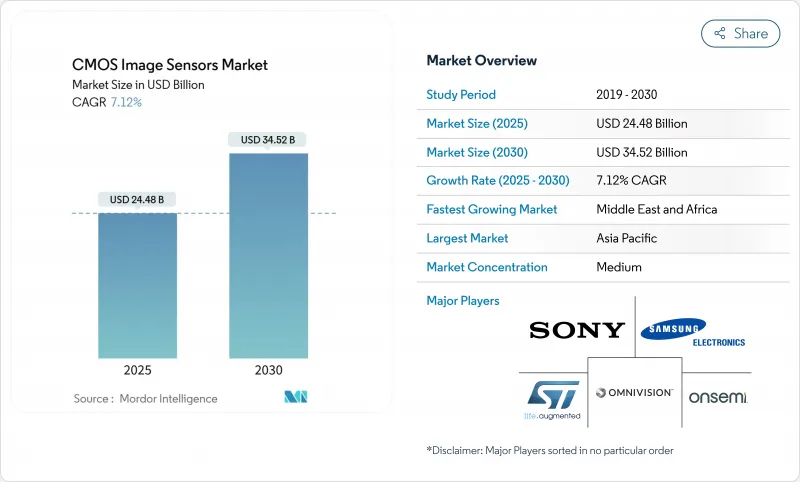
预计 CMOS 影像感测器市场规模将在 2025 年达到 245.8 亿美元,到 2030 年将达到 345.2 亿美元,复合年增长率为 7.12%。
从智慧型手机相机到汽车安全、工业自动化和医疗诊断,CMOS影像感测器的需求正在不断扩大,这反映出该技术相对于CCD设计的功能优势日益增强。采用片上AI逻辑的背照式(BSI)架构,在提升性能的同时降低了功耗,从而巩固了CMOS影像感测器在大批量电子市场的成本领先地位。从区域来看,亚太地区是台湾代工厂的主要生产动力,而中东和非洲地区则在智慧城市监控部署的推动下实现了两位数的成长。儘管美国和中国的出口限制以及300毫米晶圆的供不应求链风险,但行业整合仍在继续,传统製造商正在缩减产能并加速收购专业製造商。
全球CMOS影像感测器市场趋势与洞察
亚太地区OEM厂商采用多镜头智慧型手机
亚太地区的行动电话厂商正将多摄影机阵列从旗舰机型扩展到中阶机型,推动高动态范围影像感测器的持续成长。三星计画于2024年发表2亿像素和5,000万像素的ISOCELL感测器,凸显了其对运算摄影和高影格速率影片的重视。 OmniVision的OV50X感光元件提供110dB的单次曝光HDR,显示高阶智慧型手机的差异化优势不再仅仅体现在像素数量上,而是体现在感光元件效能上。SONY的LYT-828感测器预计将于2025年量产,其片上整合了混合帧HDR逻辑,无需外部ISP週期即可实现AI辅助的低照度处理。更高的像素密度和片上运算能力的结合,不仅支援了功能扩展,也推高了先进组件的平均售价,从而增强了CMOS影像感测器市场的收入成长。
美国和欧盟对ADAS摄影机的监管要求
美国国家公路交通安全管理局 (NHTSA) 将于 2024 年 12 月对其新车评估项目进行升级,届时轻型车辆将强制要求配备基于摄影机的盲点监测、车道维持辅助和自动紧急煞车系统,这将推动对感测器的长期需求。全域百叶窗架构能够减少运动伪影,这对安全关键型影像处理至关重要。斯巴鲁的新一代 EyeSight 系统就充分体现了这一点,该系统采用了安森美半导体 (ON Semiconductor) 的 Hyperlux AR0823AT 感测器,符合 ASIL C 安全标准。欧盟的通用安全法规与美国的要求一致,规范同步,并为 CMOS 代工厂提供了长达十年的汽车级产能投资前景。
台湾及韩国300mm CIS晶圆产能限制现状
对于台湾和韩国的代工厂而言,人工智慧晶片订单正与影像感测器生产展开竞争,导致前置作业时间从12-16週延长至20-24週。儘管台积电在亚利桑那州的扩建项目投资了1,650亿美元,但到2027年,该计画不太可能大幅缓解独联体地区的产能瓶颈。堆迭式背照式晶片製造的地理集中加剧了地缘政治风险,显着削弱了CMOS影像感测器市场近期的供应韧性。
细分市场分析
由于其卓越的灵敏度和高信噪比,背照式感测器预计在2024年将占据CMOS影像感测器市场65%的份额。这一细分市场的崛起扩大了高阶智慧型手机和车载摄影机等应用领域基于背照式(BSI)技术的CMOS影像感测器的市场规模。堆迭式BSI/3D感测器正以9.8%的复合年增长率快速发展,其整合的逻辑层可即时执行AI推理,进一步提升了每平方毫米感测器的价值。
前照式装置在成本受限的产品系列(例如入门级物联网相机)中仍将保持其重要性。全局百叶窗架构(通常基于流光溢流技术)将在工业自动化领域中得到更广泛的应用,以消除运动伪影。预计在2026年至2030年间出现的新型玻璃基板3D堆迭技术可望实现更优异的散热性能和更高的互连密度,从而扩大高阶产品的差异化优势。
到2024年,1,200万至2,400万像素频宽将占据CMOS影像感测器市场25%的份额,进而平衡主流行动装置的储存和运算开销。 4,900万像素及以上的设备虽然仍属于小众市场,但随着监控、医疗和专业摄影领域对超高倍数位变焦的需求日益增长,其市场份额正以每年9.5%的速度攀升。Canon的4.1亿像素原型机凸显了全片幅超高密度感测器的技术可行性,并有望催生新的诊断成像模式。
像素低于 1,200 万的感测器主要用于条码扫描和行车记录器等应用,在这些应用中,影格速率比清晰度更为重要。像素介于 2500 万到 4800 万之间的中端感测器则用于采用多帧计算迭加技术的无反光镜相机。像素数量的这种差异加剧了 CMOS 影像感测器市场的价格细分,并维持了利润率的差异。
区域分析
亚太地区将占2024年全球营收的34%,并受惠于从晶圆代工到最终行动装置组装的垂直整合生态系统。台湾晶圆厂供应了大部分堆迭式背照式(BSI)晶圆,而中国当地仍然是全球最大的智慧型手机出口中心。以三星ISOCELL蓝图代表的韩国创新,使其在CMOS影像感测器市场保持技术领先地位。供应链集中化带来了规模经济效益,但也增加了地震和地缘政治风险。
到2030年,中东和非洲将以9.8%的复合年增长率实现最快成长,海湾地区的智慧城市规划要求部署连网监视录影机和交通分析摄影机。配备ADAS(高级驾驶辅助系统)的车辆进口将加快售后市场的更换週期,而非洲行动优先的电子商务蓬勃发展将推动低照度自拍摄影机的需求成长。公共和私人资金筹措奖励将加速该地区的系统集成,为CMOS影像感测器市场的扩张开闢新的途径。
北美正透过社群媒体平台的需求和严格的汽车安全法规影响全球设计。内容创作生态系统优先考虑针对高影格速率8K 影片拍摄优化的感测器,这促使本土无晶圆厂供应商进入高阶细分市场。在德国工业 4.0 投资的推动下,欧洲正将光电研发转向高可靠性的工业和医疗应用。南美和南亚市场尚未开发,但价格敏感度促使采购者倾向于成熟的中阶设计,而非尖端感测器。
其他福利:
- Excel格式的市场预测(ME)表
- 3个月的分析师支持
目录
第一章 引言
- 研究假设和市场定义
- 调查范围
第二章调查方法
第三章执行摘要
第四章 市场情势
- 市场概览
- 市场驱动因素
- 亚太地区OEM厂商对多镜头智慧型手机的采用情况
- 美国和欧盟对ADAS摄影机的监管要求
- 北美以影片为中心的社群媒体对4K/8K感测器的需求
- 日本和欧盟的可穿戴小型感测器用于医疗图像诊断
- 中东智慧城市监控系统部署
- 德国工业4.0对工业自动化用全局百叶窗的需求
- 市场限制
- 台湾及韩国先进的300公厘CIS晶圆产能受限
- 入门级智慧型手机拉低了平均售价
- 高速摄影中的热噪音和滚动百叶窗限制
- 美国和中国最先进的独联体出口管制措施
- 价值/供应链分析
- 监理与技术展望
- 波特五力分析
- 供应商的议价能力
- 买方的议价能力
- 新进入者的威胁
- 替代品的威胁
- 竞争对手之间的竞争
- 技术概览(按通讯类型划分)
- 有线
- 无线的
- 投资分析
第五章 市场规模与成长预测
- 透过技术
- 前侧照明(FSI)
- 背照式(BSI)
- 堆迭式BSI/3D
- 全域百叶窗CMOS
- 通过决议
- 低于1200万像素
- 1200万至2400万像素
- 2500万至4800万像素
- 4900万像素或以上
- 频谱
- 可见频谱
- 非可见光(近红外线、紫外线、短波红外线)频谱
- 依通讯类型
- 有线
- 无线的
- 按最终用户行业划分
- 消费性电子产品
- 汽车与运输
- 工业和机器视觉
- 安全与监控
- 医疗保健和生命科学
- 计算和资料中心
- 航太/国防
- 按地区
- 北美洲
- 美国
- 加拿大
- 墨西哥
- 欧洲
- 英国
- 德国
- 法国
- 义大利
- 其他欧洲地区
- 亚太地区
- 中国
- 日本
- 印度
- 韩国
- 亚太其他地区
- 中东
- 以色列
- 沙乌地阿拉伯
- 阿拉伯聯合大公国
- 土耳其
- 其他中东地区
- 非洲
- 南非
- 埃及
- 其他非洲地区
- 南美洲
- 巴西
- 阿根廷
- 南美洲其他地区
- 北美洲
第六章 竞争情势
- 策略趋势
- 市占率分析
- 公司简介
- Sony Group Corporation
- Samsung Electronics Co., Ltd.
- OmniVision Technologies, Inc.
- onsemi Corporation
- STMicroelectronics NV
- Canon Inc.
- Panasonic Holdings Corporation
- SK Hynix Inc.
- Hamamatsu Photonics KK
- Teledyne Technologies Incorporated
- GalaxyCore Shanghai Limited Corporation
- SmartSens Technology Co., Ltd.
- PixArt Imaging Inc.
- Tower Semiconductor Ltd.
- ams-OSRAM AG
- Teledyne e2v(UK)Ltd.
- Himax Technologies, Inc.
- Siliconfile Technologies Inc.
- Sharp Corporation
- Caeleste CVBA
第七章 市场机会与未来展望
The CMOS image sensor market stands at USD 24.58 billion in 2025 and is forecast to reach USD 34.52 billion by 2030, registering a 7.12% CAGR.
Demand spreads from smartphone cameras to automotive safety, industrial automation and medical diagnostics, reflecting the technology's growing functionality advantages over CCD designs. Stacked backside-illuminated (BSI) architectures incorporating on-die AI logic raise performance while trimming power budgets, reinforcing the CMOS image sensor market's cost-leadership in mass-volume electronics. Regionally, Asia-Pacific anchors production through Taiwan's foundries, while Middle East and Africa outpace with double-digit expansion on smart-city surveillance deployments. Consolidation continues as legacy producers divest capacity and specialist acquisitions accelerate, even as U.S.-China export controls and 300 mm wafer shortages inject supply-chain risk.
Global CMOS Image Sensors Market Trends and Insights
Smartphone Multi-Camera Adoption by APAC OEMs
APAC handset makers are extending multi-camera arrays from flagships into mid-range lines, driving sustained unit growth for high-dynamic-range image sensors. Samsung's 2024 release of 200 MP and 50 MP ISOCELL devices underscored the pivot toward computational photography and higher frame-rate video. OmniVision's OV50X, offering 110 dB single-exposure HDR, illustrates how premium smartphones now differentiate on sensor capability rather than megapixel count alone. Sony's LYT-828, entering mass production in 2025, embeds Hybrid Frame-HDR logic on-die, allowing AI-assisted low-light processing without external ISP cycles. The combination of higher pixel densities and on-sensor compute supports feature expansion while raising average selling prices for advanced parts, reinforcing revenue growth for the CMOS image sensor market.
Regulatory Mandates for ADAS Cameras in US & EU
NHTSA's December 2024 New Car Assessment Program upgrade mandates camera-based blind-spot, lane-keeping and automatic emergency-braking systems across light vehicles, anchoring long-term sensor demand. Global-shutter architectures mitigate motion artifacts essential for safety-critical imaging, evident in Subaru's next-generation EyeSight system that selects onsemi's Hyperlux AR0823AT sensor meeting ASIL C safety standards. The EU's General Safety Regulation mirrors U.S. requirements, synchronizing specifications and giving CMOS foundry operators visibility for a decade of automotive-grade capacity investments.
Advanced 300 mm CIS Wafer Capacity Constraints in Taiwan & Korea
Surging AI-chip orders compete with image-sensor output for advanced 300 mm lines at Taiwanese and Korean foundries, extending lead times from 12-16 weeks to 20-24 weeks. TSMC's Arizona expansion, though capitalized at USD 165 billion, will not meaningfully relieve CIS bottlenecks before 2027. The geographic clustering of stacked BSI manufacturing heightens geopolitical exposure, significantly tempering near-term supply elasticity for the CMOS image sensor market.
Other drivers and restraints analyzed in the detailed report include:
- Video-Centric Social-Media Demand for 4K/8K Sensors in North America
- Miniaturized Sensors for Wearable Medical Imaging in Japan & EU
- ASP Erosion in Entry-Level Smartphones
For complete list of drivers and restraints, kindly check the Table Of Contents.
Segment Analysis
Backside-illuminated sensors captured 65% CMOS image sensor market share in 2024, reflecting superior sensitivity and higher signal-to-noise ratios. The segment's ascendancy lifted the BSI-based CMOS image sensor market size for premium smartphones and automotive cameras. Stacked BSI/3D sensors are advancing at 9.8% CAGR, integrating logic layers that execute AI inference in situ and further enlarge value per square millimeter.
Front-side-illuminated devices maintain relevance in cost-constrained SKUs such as entry-level IoT cameras. Global-shutter architectures, often FSI-based, gain adoption in industrial automation to thwart motion artefacts. Emerging glass-substrate 3D stacking, projected between 2026 and 2030, promises tighter thermal profiles and higher interconnect densities, widening high-end differentiation.
The 12-24 MP band accounted for 25% CMOS image sensor market share in 2024, balancing storage and compute overhead in mainstream handsets. >=49 MP devices, though niche, are growing 9.5% annually as surveillance, medical and professional photography favor extreme digital zoom. Canon's 410 MP prototype highlights technical viability of full-frame ultra-high-density sensors, potentially catalyzing new diagnostic imaging modalities.
Sub-12 MP parts endure in barcode scanning and dashcams where frame rate trumps definition. Mid-tier 25-48 MP sensors serve mirrorless cameras leveraging multi-frame computational overlays. The pixel-count bifurcation sharpens price segmentation across the CMOS image sensor market, preserving margin tiers.
The CMOS Image Sensor Market Report is Segmented by Technology (Front Side Illuminated, Backside-Illuminated, and More), Resolution ( Less Than 12 Megapixels, 12-24 Megapixels, and More ), Spectrum (Visible, Non-Visible), Communication Type (Wired, Wireless), End-User Industry (Consumer Electronics, Automotive, Industrial, and More), and Geography. The Market Forecasts are Provided in Terms of Value (USD).
Geography Analysis
Asia-Pacific holds 34% of 2024 revenue, benefiting from vertically integrated ecosystems spanning foundry silicon to final handset assembly. Taiwanese fabs supply the bulk of stacked-BSI wafers, while mainland China remains the world's largest smartphone export base. Korean innovation, led by Samsung's ISOCELL roadmap, sustains technology leadership inside the CMOS image sensor market. Supply-chain concentration confers scale economics yet elevates earthquake and geopolitical exposure.
Middle East and Africa present the fastest growth at 9.8% CAGR to 2030 as Gulf smart-city blueprints demand networked surveillance and traffic-analytics cameras. ADAS-equipped vehicle imports lift aftermarket replacement cycles, while Africa's mobile-first e-commerce boom drives low-light selfie camera volumes. Public-private funding incentives accelerate local system integration, creating an emerging corridor for CMOS image sensor market expansion.
North America influences global design through social-media platform demands and stringent automotive safety rules. Content-creator ecosystems prioritize sensors optimized for high-frame-rate 8K capture, pushing domestic fabless vendors toward premium niches. Europe, anchored by Germany's Industry 4.0 investments, channels photonics R&D into high-reliability industrial and medical segments. South America and South Asia represent untapped volume, though price sensitivity steers procurement toward established mid-tier designs rather than bleeding-edge sensors.
- Sony Group Corporation
- Samsung Electronics Co., Ltd.
- OmniVision Technologies, Inc.
- onsemi Corporation
- STMicroelectronics N.V.
- Canon Inc.
- Panasonic Holdings Corporation
- SK Hynix Inc.
- Hamamatsu Photonics K.K.
- Teledyne Technologies Incorporated
- GalaxyCore Shanghai Limited Corporation
- SmartSens Technology Co., Ltd.
- PixArt Imaging Inc.
- Tower Semiconductor Ltd.
- ams-OSRAM AG
- Teledyne e2v (UK) Ltd.
- Himax Technologies, Inc.
- Siliconfile Technologies Inc.
- Sharp Corporation
- Caeleste CVBA
Additional Benefits:
- The market estimate (ME) sheet in Excel format
- 3 months of analyst support
TABLE OF CONTENTS
1 INTRODUCTION
- 1.1 Study Assumptions and Market Definition
- 1.2 Scope of the Study
2 RESEARCH METHODOLOGY
3 EXECUTIVE SUMMARY
4 MARKET LANDSCAPE
- 4.1 Market Overview
- 4.2 Market Drivers
- 4.2.1 Smartphone Multi-Camera Adoption by APAC OEMs
- 4.2.2 Regulatory Mandates for ADAS Cameras in US and EU
- 4.2.3 Video-Centric Social Media Demand for 4K/8K Sensors in North America
- 4.2.4 Miniaturized Sensors for Wearable Medical Imaging in Japan and EU
- 4.2.5 Smart-City Surveillance Roll-outs in Middle East
- 4.2.6 Global-Shutter Demand for Industrial Automation in Germany's Industry 4.0
- 4.3 Market Restraints
- 4.3.1 Advanced 300-mm CIS Wafer Capacity Constraints in Taiwan and Korea
- 4.3.2 ASP Erosion in Entry-Level Smartphones
- 4.3.3 Thermal Noise and Rolling-Shutter Limits in High-Speed Cinematography
- 4.3.4 US-China Export Controls on Leading-Edge CIS
- 4.4 Value / Supply-Chain Analysis
- 4.5 Regulatory and Technological Outlook
- 4.6 Porter's Five Forces Analysis
- 4.6.1 Bargaining Power of Suppliers
- 4.6.2 Bargaining Power of Buyers
- 4.6.3 Threat of New Entrants
- 4.6.4 Threat of Substitutes
- 4.6.5 Intensity of Competitive Rivalry
- 4.7 Technology Snapshot (By Communication Type)
- 4.7.1 Wired
- 4.7.2 Wireless
- 4.8 Investment Analysis
5 MARKET SIZE AND GROWTH FORECASTS (VALUE)
- 5.1 By Technology
- 5.1.1 Front-Side Illuminated (FSI)
- 5.1.2 Backside-Illuminated (BSI)
- 5.1.3 Stacked BSI / 3-D
- 5.1.4 Global-Shutter CMOS
- 5.2 By Resolution
- 5.2.1 Less than 12 Megapixels
- 5.2.2 12-24 Megapixels
- 5.2.3 25-48 Megapixels
- 5.2.4 Greater than 49 Megapixels
- 5.3 By Spectrum
- 5.3.1 Visible Spectrum
- 5.3.2 Non-Visible (NIR, UV, SWIR) Spectrum
- 5.4 By Communication Type
- 5.4.1 Wired
- 5.4.2 Wireless
- 5.5 By End-user Industry
- 5.5.1 Consumer Electronics
- 5.5.2 Automotive and Transportation
- 5.5.3 Industrial and Machine Vision
- 5.5.4 Security and Surveillance
- 5.5.5 Healthcare and Life Sciences
- 5.5.6 Computing and Data-center
- 5.5.7 Aerospace and Defense
- 5.6 By Geography
- 5.6.1 North America
- 5.6.1.1 United States
- 5.6.1.2 Canada
- 5.6.1.3 Mexico
- 5.6.2 Europe
- 5.6.2.1 United Kingdom
- 5.6.2.2 Germany
- 5.6.2.3 France
- 5.6.2.4 Italy
- 5.6.2.5 Rest of Europe
- 5.6.3 Asia-Pacific
- 5.6.3.1 China
- 5.6.3.2 Japan
- 5.6.3.3 India
- 5.6.3.4 South Korea
- 5.6.3.5 Rest of Asia-Pacific
- 5.6.4 Middle East
- 5.6.4.1 Israel
- 5.6.4.2 Saudi Arabia
- 5.6.4.3 United Arab Emirates
- 5.6.4.4 Turkey
- 5.6.4.5 Rest of Middle East
- 5.6.5 Africa
- 5.6.5.1 South Africa
- 5.6.5.2 Egypt
- 5.6.5.3 Rest of Africa
- 5.6.6 South America
- 5.6.6.1 Brazil
- 5.6.6.2 Argentina
- 5.6.6.3 Rest of South America
- 5.6.1 North America
6 COMPETITIVE LANDSCAPE
- 6.1 Strategic Moves
- 6.2 Market Share Analysis
- 6.3 Company Profiles (includes Global level Overview, Market level overview, Core Segments, Financials as available, Strategic Information, Market Rank/Share for key companies, Products and Services, and Recent Developments)
- 6.3.1 Sony Group Corporation
- 6.3.2 Samsung Electronics Co., Ltd.
- 6.3.3 OmniVision Technologies, Inc.
- 6.3.4 onsemi Corporation
- 6.3.5 STMicroelectronics N.V.
- 6.3.6 Canon Inc.
- 6.3.7 Panasonic Holdings Corporation
- 6.3.8 SK Hynix Inc.
- 6.3.9 Hamamatsu Photonics K.K.
- 6.3.10 Teledyne Technologies Incorporated
- 6.3.11 GalaxyCore Shanghai Limited Corporation
- 6.3.12 SmartSens Technology Co., Ltd.
- 6.3.13 PixArt Imaging Inc.
- 6.3.14 Tower Semiconductor Ltd.
- 6.3.15 ams-OSRAM AG
- 6.3.16 Teledyne e2v (UK) Ltd.
- 6.3.17 Himax Technologies, Inc.
- 6.3.18 Siliconfile Technologies Inc.
- 6.3.19 Sharp Corporation
- 6.3.20 Caeleste CVBA
7 MARKET OPPORTUNITIES AND FUTURE OUTLOOK
- 7.1 White-Space and Unmet-Need Assessment
 CMOS影像感测器市场预测至2032年:按类型、频谱、解析度、影像处理技术、最终用户和地区分類的分析
 CMOS相机模组市场(按应用、产品类型、最终用户、介面类型和解析度)—全球预测 2025-2032
 2025-2029年全球製药业CMO市场
 2025-2029年全球CMOS相机模组市场
 有机 CMOS 影像感测器市场规模、份额、成长分析,按影像处理、按阵列类型、按应用、按行业部门、按地区 - 产业预测,2025 年至 2032 年
 全球 CMOS 影像感测器市场:市场规模、市场份额和趋势分析(按频谱、影像处理技术、解析度、最终用途和地区)、按细分市场预测(2025-2030 年)
 CMOS SCMOS 影像感测器市场 - 全球产业规模、份额、趋势、机会和预测,按技术、规格、晶圆尺寸、感测器尺寸、应用、地区和竞争细分,2019-2029F
 CMOS影像感测器的全球市场:洞察·预测 (~2030年)全球 CMOS 影像感测器市场:按类型、应用和最终用户产业划分 - 预测 2024-2030 年