


 |
市场调查报告书
商品编码
1906136
光阻剂:市场占有率分析、产业趋势与统计、成长预测(2026-2031)Photoresist - Market Share Analysis, Industry Trends & Statistics, Growth Forecasts (2026 - 2031) |
||||||
※ 本网页内容可能与最新版本有所差异。详细情况请与我们联繫。
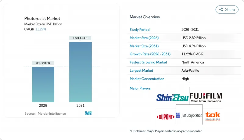
预计到 2025 年,光阻剂市场价值将达到 26 亿美元,到 2031 年将达到 49.4 亿美元,高于 2026 年的 28.9 亿美元。
预计在预测期(2026-2031 年)内,复合年增长率将达到 11.29%。
推动这项扩张的因素包括:极紫外线 (EUV) 光刻技术在亚10奈米特征尺寸製造中的广泛应用、人工智慧 (AI) 加速器需求的激增以及政府主导的晶圆厂激励措施。台湾、韩国和美国的半导体製造商正越来越多地采用抗蚀剂高 EUV 吸收率和低线边缘粗糙度的金属氧化物和光阻剂,从而提高生产效率并降低每层抗蚀剂的使用量。 5G 和物联网 (IoT) 设备的同步发展也持续推动成熟节点对 G 线、I 线和 KrF 材料的需求。同时,晶片组、扇出型晶圆层次电子构装和光学共封装等先进封装结构需要与铜柱和硅通孔 (TSV) 结构相容的厚膜抗蚀剂。供应链风险仍然较高,三家日本製造商占据了先进抗蚀剂的约 60%,促使北美和欧洲的製造商进行地域多角化,并提高本地产能。
全球光阻剂市场趋势及展望
来自半导体和人工智慧加速器的需求不断增长
目前,晶片製造商为大规模语言模型训练和推理工作负载生产硬体时,通常会在每个装置上整合多个线路重布、中介层和硅通孔(TSV)。 NVIDIA 的 H100 和即将推出的 Blackwell 系列采用晶片组布局,其每个成品装置的光阻剂消耗量是传统单晶片 GPU 的三到五倍。台积电(TSMC)扩大其晶片封装(CoWoS)产能,推动了对厚度达 50 微米的抗蚀剂的需求。同时,先进的铜柱电镀技术采用针对 3:1 或更大长宽比优化的负性光阻配方。产能扩张最初将在台湾和韩国进行,预计到 2027 年将扩展到美国的新晶圆厂。
加速EUV微影术应用与高数值孔径蓝图
ASML 的 0.55NA EUV 曝光工具可实现 8nm 间距的单次曝光图形化,无需高成本的多次图形化步骤。为了满足更严格的线边缘粗糙度目标(小于 1.5nm),晶圆厂采用了基于铪锆丛集的金属氧化物抗蚀剂,其 EUV 光吸收效率是有机抗蚀剂的九倍。这使得曝光剂量从 40 mJ/cm² 降低到小于 20 mJ/cm²,从而提高了生产效率并降低了单片晶圆的成本。根据 2025 年在三星平泽生产线进行的试点运行结果,预计 2026 年在 2nm 製程节点上实现商业部署。
关于溶剂和光酸发生器的严格健康、安全和环境 (HSE) 法规
2024年,欧盟修订了2024/573号法规,计画在2045年逐步淘汰90%的氢氟碳化合物。目前,许多极紫外光光阻剂使用全氟化光酸发生剂和溶剂,这些物质需要经过註册、评估和批准。合规要求对杂质含量低于1 ppb进行分析检验,这增加了品管成本,并迫使配方师测试替代化学方法,而这会带来性能下降的风险。
细分市场分析
受台积电、三星和英特尔等厂商对7nm和5nm製程的持续需求推动,ArF浸没式光阻剂预计在2025年将维持31.85%的光阻剂市场份额。同时,随着晶圆厂向2nm逻辑製程转型,金属氧化物抗蚀剂和EUV干式抗蚀剂预计将创造最大的增量价值,年复合成长率将达到12.94%。铪基丛集的抗蚀刻性能是普通有机聚合物的25倍以上,无需硬掩模即可直接转移到介电层,从而缩短製程。
Lam Research 的干式沉积光阻抗蚀剂消除旋涂製程的废弃物,并将化学品消费量降低高达 90%。该平台计划于 2026 年实现量产,预计将材料收入从湿化学品供应商转移到设备整合供应商。 KrF、G 系列和 I 系列抗蚀剂在汽车和工业领域仍然至关重要,随着先进製程节点推动成长,它们将为公司提供稳定的基础收入。
到 2025 年,正性光阻材料占光阻剂市场的 71.45%。负性抗蚀剂,尤其是环氧树脂和金属氧化物基光阻,预计到 2031 年将以 11.38% 的复合年增长率增长,这主要得益于先进封装中对更厚薄膜层的需求激增。
负性抗蚀剂能够承受铜柱电镀过程中的高电流密度,从而实现长宽比,这对于形成小间距凸点至关重要。新兴的双色调氧化锡平台透过剂量控制的色调切换,提供了製程柔软性。 imec的初步测试表明,在20mJ/cm²的曝光剂量下,分辨率可低于16nm。
区域分析
预计到2025年,亚太地区在全球营收中所占份额将达到72.10%,这主要得益于台湾和韩国高密度逻辑晶片产能的扩张,以及中国成熟节点晶圆厂的建设。台积电面向高效能运算的2nm製程量产和封装生产线推动了EUV光阻和厚膜材料的消费量成长,而三星的3D NAND快闪记忆体产能则带动了对高选择性KrF抗蚀剂的需求。日本的设备生态系统、东京电子的镀膜设备以及尼康的步进光刻机为日本国内供应商提供了支持,形成了一条紧密整合的供应链。
在北美,《晶片製造和整合法案》(CHIPS Act)的实施将促进新建待开发区的建设,预计到2031年,其年复合成长率将达到11.49%。到2028年,英特尔位于俄亥俄州的园区、台积电位于亚利桑那州的工厂以及三星位于德克萨斯州的工厂将总合超过30万晶圆/分钟的先进产能,以满足该地区对抗蚀剂及相关化学品的需求。杜邦位于科罗拉多的扩建项目和陶氏位于密西根州的扩建项目旨在为该地区提供产品,并降低跨太平洋物流风险。
在欧洲,严格遵守REACH法规将推高配方成本,而英特尔在爱尔兰的大规模投资以及在德国的建设计画计画将起到推动作用。当地材料供应商默克集团和BASF正利用其在法规方面的专业知识,为EUV生产线争取认证。东欧国家则致力于吸引封装和测试业务,以实现地理布局的多元化。
中东、非洲和南美洲是发展中地区,但它们正在大力推动先进封装和微机电系统(MEMS)製造,尤其是在电信基地台和汽车感测器领域。这些地区政府提供税收优惠以吸引后端组装,从而提振了对G线和I线工艺光阻剂的需求,但先进製程节点仍集中在其他地区。
其他福利:
- Excel格式的市场预测(ME)表
- 分析师支持(3个月)
目录
第一章 引言
- 研究假设和市场定义
- 调查范围
第二章调查方法
第三章执行摘要
第四章 市场情势
- 市场概览
- 市场驱动因素
- 来自半导体和人工智慧加速器的需求不断增长
- 加速采用EUV微影技术及高数值孔径蓝图
- 由于5G/物联网设备的广泛应用,晶圆产量增加。
- 政府晶圆厂奖励计画(美国/欧盟晶片法案)
- 干式沉积金属氧化物抗蚀剂可提高极紫外光刻效率
- 市场限制
- 溶剂和光酸发生器的严格健康、安全和环境法规
- 供应链集中度与出口管制风险
- 逐步淘汰欧盟REACH法规和针对含氟溶剂的氟碳法规
- 价值链分析
- 监管环境
- 波特五力模型
- 供应商的议价能力
- 买方的议价能力
- 新进入者的威胁
- 替代品的威胁
- 竞争程度
第五章 市场规模与成长预测
- 抗蚀剂类型
- ArF浸入式
- ArF 干式
- KrF
- G-Line
- I 线
- 用于极紫外光刻的金属氧化物和干式抗蚀剂
- 其他类型
- 按音调
- 积极的
- 消极的
- 透过使用
- 半导体和积体电路(IC)
- 先进封装(扇出型 WLP、RDL)
- 平板显示器(LCD/ 有机发光二极体)
- 印刷基板
- 微机电系统和感测器
- 其他用途
- 按最终用户行业划分
- 电子电器设备
- 汽车与出行
- 航太/国防
- 消费品(包装)
- 其他行业
- 按地区
- 亚太地区
- 中国
- 日本
- 韩国
- 台湾
- 印度
- 亚太其他地区
- 北美洲
- 美国
- 加拿大
- 墨西哥
- 欧洲
- 德国
- 英国
- 法国
- 义大利
- 俄罗斯
- 其他欧洲地区
- 南美洲
- 巴西
- 阿根廷
- 南美洲其他地区
- 中东和非洲
- 沙乌地阿拉伯
- 阿拉伯聯合大公国
- 南非
- 其他中东和非洲地区
- 亚太地区
第六章 竞争情势
- 市场集中度
- 策略趋势
- 市占率(%)/排名分析
- 公司简介
- ALLRESIST GmbH
- Asahi Kasei Corporation
- Avantor, Inc.
- Brewer Science, Inc.
- DJ MicroLaminates
- DONGJIN SEMICHEM CO. LTD
- DuPont
- Eternal Materials Co., Ltd.
- FUJIFILM Corporation
- Inpria
- JSR Corporation
- SEMI
- Kolon Industries, Inc.
- LG Chem
- Merck KGaA
- micro resist technology GmbH
- Microchemicals GmbH
- Shin-Etsu Chemical Co., Ltd.
- Sumitomo Chemical Co., Ltd.
- TOKYO OHKA KOGYO CO., LTD.
- Jiangsu Nata Opto-electronic Material Co., Ltd.
第七章 市场机会与未来展望
The Photoresist Market was valued at USD 2.60 billion in 2025 and estimated to grow from USD 2.89 billion in 2026 to reach USD 4.94 billion by 2031, at a CAGR of 11.29% during the forecast period (2026-2031).
The widespread deployment of extreme-ultraviolet (EUV) lithography at sub-10-nanometer dimensions, the fast-growing demand for artificial-intelligence (AI) accelerators, and government-funded fab incentives underpin this expansion. Semiconductor manufacturers in Taiwan, South Korea, and the United States are increasingly favoring metal-oxide and dry photoresists that deliver higher EUV absorption and lower line-edge roughness, thereby boosting throughput and reducing per-layer resist usage. Parallel momentum in 5G and Internet-of-Things (IoT) devices sustains demand for mature-node G-line, I-line, and KrF materials. Meanwhile, advanced packaging architectures-such as chiplets, fan-out wafer-level packaging, and co-packaged optics-require thick-film resists that are compatible with copper pillar and through-silicon-via (TSV) structures. Supply-chain risks remain elevated because three Japanese suppliers collectively account for roughly 60% of advanced resists, prompting regional diversification and localized capacity additions in North America and Europe.
Global Photoresist Market Trends and Insights
Growing Demand from Semiconductor and AI Accelerators
Chipmakers producing hardware for training large language models and powering inference workloads now pattern multiple redistribution layers, interposers, and TSVs for each device. NVIDIA's H100 and forthcoming Blackwell series adopt chiplet layouts that consume three to five times more photoresist per finished part than previous monolithic GPUs. Taiwan Semiconductor Manufacturing Company's (TSMC) expansion of CoWoS capacity lifts thick-film resist of up to 50 µm, while advanced copper pillar plating uses negative-tone formulations optimized for aspect ratios above 3:1. Volume gains occur first in Taiwan and South Korea but ripple into new fabs in the United States by 2027.
Accelerated EUV Lithography Adoption and High-NA Roadmap
ASML's 0.55-NA EUV scanners enable single-exposure patterning with an 8 nm pitch, eliminating costly multiple-patterning steps. To meet the tighter line-edge roughness target of below 1.5 nm, fabs qualify metal-oxide resists based on hafnium and zirconium clusters that absorb EUV 9 times more effectively than organic formulations . The dose can be reduced from 40 mJ/cm2 to sub-20 mJ/cm2, increasing throughput and lowering the cost per wafer. Pilot runs at Samsung's Pyeongtaek lines in 2025 suggest commercial adoption at 2 nm nodes in 2026.
Stringent HSE Regulations on Solvents and Photo-Acid Generators
The European Union's 2024 revision to Regulation (EU) 2024/573 schedules a phase-down of hydrofluorocarbon usage by 90% before 2045. Many EUV photoresists now employ perfluorinated photoacid generators and solvents, which are subject to registration, evaluation, and authorization. Compliance requires analytical verification of impurity levels below 1 ppb, which drives up quality-control costs and forces formulators to test alternative chemistries that may risk lower performance.
Other drivers and restraints analyzed in the detailed report include:
- 5G/IoT Device Proliferation Expanding Wafer Starts
- Government Fab-Incentive Programs (US/EU Chips Acts)
- Supply-Chain Concentration and Export-Control Exposure
For complete list of drivers and restraints, kindly check the Table Of Contents.
Segment Analysis
ArF immersion formulations retained a 31.85% share of the photoresist market size in 2025, thanks to sustained demand for 7 nm and 5 nm volumes at TSMC, Samsung, and Intel. Conversely, EUV metal-oxide and dry resists are projected to post a 12.94% CAGR, generating the largest incremental value as fabs transition to 2 nm logic. Hafnium-based clusters deliver etch resistance exceeding 25 times that of organic polymers, enabling direct transfer into dielectric layers without a hard mask and thus shortening the process flow.
Lam Research's dry-deposited resist eliminates spin waste and cuts chemical consumption by up to 90%. With mass production targeted for 2026, this platform could shift material revenue from wet-chemistry suppliers toward equipment-integrated delivery. KrF, G-line, and I-line resists remain essential for automotive and industrial nodes, anchoring a steady base revenue even as advanced nodes dominate growth.
Positive-tone materials dominated the photoresist market with a 71.45% share in 2025. Negative-tone resists, particularly epoxy-based and metal-oxide systems, are forecast to rise at 11.38% CAGR through 2031 as demand for high-thickness layers in advanced packaging surges.
Negative resists withstand high current densities during copper-pillar plating and achieve aspect ratios exceeding 3:1, which is critical for fine-pitch bump formation. Emerging dual-tone tin-oxide platforms offer process flexibility by switching tone with dose control; early tests at imec show sub-16 nm resolution at 20 mJ/cm2 exposure.
The Photoresist Market Report is Segmented by Resist Type (ArF Immersion and More), Tone (Positive and Negative), Application (Semiconductors and ICs and More), End-User Industry (Electronics and Electricals and More), and Geography (Asia-Pacific, North America, Europe, South America, and Middle-East and Africa). The Market Forecasts are Provided in Terms of Value (USD).
Geography Analysis
The Asia-Pacific region accounted for 72.10% of global revenue in 2025, driven by dense logic capacity in Taiwan and South Korea, as well as the expansion of mature-node fabs in China. TSMC's 2nm ramp and high-performance computing package lines consume increasing volumes of EUV and thick-film materials, while Samsung's 3D NAND capacity drives demand for high-selectivity KrF resists. Japan's equipment ecosystem, Tokyo Electron coating tracks, and Nikon steppers, support domestic suppliers, creating a tightly integrated supply chain.
North America is forecast to record an 11.49% CAGR through 2031 as the CHIPS Act stimulates the construction of new greenfield fabs. Intel's Ohio campus, TSMC's Arizona site, and Samsung's Texas facility together add more than 300,000 wpm of leading-edge capacity by 2028, underpinning local resist and ancillary chemical demand. DuPont's Colorado expansion and Dow's Michigan expansion aim to supply the region and reduce trans-Pacific logistics risk.
Europe faces stringent REACH compliance, which raises formulation costs, yet benefits from Intel's large-scale investment in Ireland and prospective fabs in Germany. Local material suppliers, Merck KGaA and BASF, utilize their regulatory expertise to secure qualification for EUV lines. Eastern European countries court packaging and test operations, further diversifying the regional footprint.
Middle East & Africa and South America remain nascent but pursue specialty packaging and MEMS manufacturing, particularly for telecom base-stations and automotive sensors. Regional governments offer tax credits to attract backend assembly, bringing incremental photoresist volumes for G-line and I-line processes while advanced nodes stay concentrated elsewhere.
- ALLRESIST GmbH
- Asahi Kasei Corporation
- Avantor, Inc.
- Brewer Science, Inc.
- DJ MicroLaminates
- DONGJIN SEMICHEM CO. LTD
- DuPont
- Eternal Materials Co., Ltd.
- FUJIFILM Corporation
- Inpria
- JSR Corporation
- SEMI
- Kolon Industries, Inc.
- LG Chem
- Merck KGaA
- micro resist technology GmbH
- Microchemicals GmbH
- Shin-Etsu Chemical Co., Ltd.
- Sumitomo Chemical Co., Ltd.
- TOKYO OHKA KOGYO CO., LTD.
- Jiangsu Nata Opto-electronic Material Co., Ltd.
Additional Benefits:
- The market estimate (ME) sheet in Excel format
- 3 months of analyst support
TABLE OF CONTENTS
1 Introduction
- 1.1 Study Assumptions & Market Definition
- 1.2 Scope of the Study
2 Research Methodology
3 Executive Summary
4 Market Landscape
- 4.1 Market Overview
- 4.2 Market Drivers
- 4.2.1 Growing demand from semiconductor and AI accelerators
- 4.2.2 Accelerated EUV lithography adoption and High-NA roadmap
- 4.2.3 5G / IoT device proliferation expanding wafer starts
- 4.2.4 Government fab-incentive programs (US/EU Chips Acts)
- 4.2.5 Dry-deposited metal-oxide resists boosting EUV throughput
- 4.3 Market Restraints
- 4.3.1 Stringent HSE regulations on solvents and photo-acid generators
- 4.3.2 Supply-chain concentration and export-control exposure
- 4.3.3 EU REACH and F-gas phase-outs targeting fluorinated solvents
- 4.4 Value Chain Analysis
- 4.5 Regulatory Landscape
- 4.6 Porter's Five Forces
- 4.6.1 Bargaining Power of Suppliers
- 4.6.2 Bargaining Power of Buyers
- 4.6.3 Threat of New Entrants
- 4.6.4 Threat of Substitutes
- 4.6.5 Degree of Competition
5 Market Size & Growth Forecasts (Value)
- 5.1 By Resist Type
- 5.1.1 ArF Immersion
- 5.1.2 ArF Dry
- 5.1.3 KrF
- 5.1.4 G-Line
- 5.1.5 I-Line
- 5.1.6 EUV Metal-Oxide and Dry Resists
- 5.1.7 Other Types
- 5.2 By Tone
- 5.2.1 Positive
- 5.2.2 Negative
- 5.3 By Application
- 5.3.1 Semiconductors and ICs
- 5.3.2 Advanced Packaging (Fan-Out WLP, RDL)
- 5.3.3 Flat-Panel Displays (LCD/OLED)
- 5.3.4 Printed Circuit Boards
- 5.3.5 MEMS and Sensors
- 5.3.6 Other Applications
- 5.4 By End-User Industry
- 5.4.1 Electronics and Electricals
- 5.4.2 Automotive and Mobility
- 5.4.3 Aerospace and Defense
- 5.4.4 Consumer Packaged Goods (Packaging)
- 5.4.5 Other Industries
- 5.5 By Geography
- 5.5.1 Asia-Pacific
- 5.5.1.1 China
- 5.5.1.2 Japan
- 5.5.1.3 South Korea
- 5.5.1.4 Taiwan
- 5.5.1.5 India
- 5.5.1.6 Rest of Asia-Pacific
- 5.5.2 North America
- 5.5.2.1 United States
- 5.5.2.2 Canada
- 5.5.2.3 Mexico
- 5.5.3 Europe
- 5.5.3.1 Germany
- 5.5.3.2 United Kingdom
- 5.5.3.3 France
- 5.5.3.4 Italy
- 5.5.3.5 Russia
- 5.5.3.6 Rest of Europe
- 5.5.4 South America
- 5.5.4.1 Brazil
- 5.5.4.2 Argentina
- 5.5.4.3 Rest of South America
- 5.5.5 Middle-East and Africa
- 5.5.5.1 Saudi Arabia
- 5.5.5.2 United Arab Emirates
- 5.5.5.3 South Africa
- 5.5.5.4 Rest of Middle-East and Africa
- 5.5.1 Asia-Pacific
6 Competitive Landscape
- 6.1 Market Concentration
- 6.2 Strategic Moves
- 6.3 Market Share (%)/Ranking Analysis
- 6.4 Company Profiles (includes Global-level Overview, Market-level Overview, Core Segments, Financials, Strategic Information, Market Rank/Share, Products & Services, Recent Developments)
- 6.4.1 ALLRESIST GmbH
- 6.4.2 Asahi Kasei Corporation
- 6.4.3 Avantor, Inc.
- 6.4.4 Brewer Science, Inc.
- 6.4.5 DJ MicroLaminates
- 6.4.6 DONGJIN SEMICHEM CO. LTD
- 6.4.7 DuPont
- 6.4.8 Eternal Materials Co., Ltd.
- 6.4.9 FUJIFILM Corporation
- 6.4.10 Inpria
- 6.4.11 JSR Corporation
- 6.4.12 SEMI
- 6.4.13 Kolon Industries, Inc.
- 6.4.14 LG Chem
- 6.4.15 Merck KGaA
- 6.4.16 micro resist technology GmbH
- 6.4.17 Microchemicals GmbH
- 6.4.18 Shin-Etsu Chemical Co., Ltd.
- 6.4.19 Sumitomo Chemical Co., Ltd.
- 6.4.20 TOKYO OHKA KOGYO CO., LTD.
- 6.4.21 Jiangsu Nata Opto-electronic Material Co., Ltd.
7 Market Opportunities and Future Outlook
- 7.1 White-space and Unmet-Need Assessment
 2026年混合对数伽玛(HLG)光电显示支架全球市场报告
 IC光阻剂市场:按技术、类型、形式、基板、应用和最终用户划分-全球预测,2026-2032年KrF光阻剂市场(半导体领域):按类型、组件、技术节点、应用和最终用户产业划分-2026年至2032年全球预测TFT-LCD光阻剂市场:按类型、成分、曝光方法、製程、应用、最终用途和销售管道-全球预测,2026-2032年显示光阻剂市场:按类型、技术、涂覆方法、应用和最终用途划分-2026-2032年全球预测正性光阻剂市场:按抗蚀剂类型、製程、厚度范围、应用和最终用途产业划分-2026-2032年全球预测KrF抗蚀剂市场按化学成分、技术节点、应用方法、应用领域和最终用户划分-2026-2032年全球预测光阻剂市场按技术、材料类型、产品类型、波长和应用划分-2026-2032年全球预测半导体光阻剂市场:2026-2032年全球预测(按抗蚀剂类型、化学成分、技术节点、晶圆尺寸、曝光技术、产品形式和应用划分)
 光阻剂市场规模、份额及成长分析(按类型、助剂类型、应用和地区划分)-2026-2033年产业预测