


 |
市场调查报告书
商品编码
1940878
硅电容器:市场占有率分析、产业趋势与统计、成长预测(2026-2031)Silicon Capacitors - Market Share Analysis, Industry Trends & Statistics, Growth Forecasts (2026 - 2031) |
||||||
※ 本网页内容可能与最新版本有所差异。详细情况请与我们联繫。
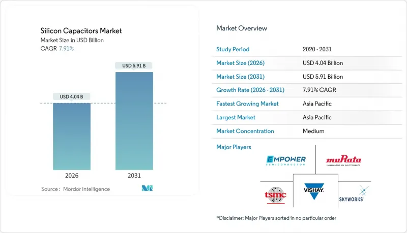
预计硅电容器市场将从 2025 年的 37.4 亿美元成长到 2026 年的 40.4 亿美元,到 2031 年将达到 59.1 亿美元,2026 年至 2031 年的复合年增长率为 7.91%。
这一成长反映了5G和下一代6G设备对高密度射频前端设计的快速采用、向高温汽车雷射雷达模组的转变,以及对具有嵌入式深沟槽电容器的基于晶片组的2.5D中介层的强劲需求。代工厂为先进被动元件分配的新生产线提高了碳奈米纤维MIM结构的供应稳定性,并缓解了先前的成本上升趋势。亚太地区凭藉其一体化的晶圆製造基地和积极的无线基础设施部署,保持着明显的生产优势。同时,北美正在抢占来自工作频率高于100GHz的国防级平板阵列的高端市场需求。随着传统被动元件供应商努力抵御代工厂将嵌入式电容器与逻辑晶粒捆绑在一起的产品,竞争格局日益激烈。这导致大批量智慧型手机产品的毛利率下降,但恶劣环境细分市场仍保持着成长潜力。
全球硅电容器市场趋势与洞察
加速5G/6G终端射频前端的小型化
与4G设计相比,下一代智慧型手机将整合40-60%的电容元件,这将迫使OEM厂商从陶瓷MLCC转向硅介质,进而降低6-40GHz频段的寄生电感。村田製作所于2025年3月发布的数位封包追踪平台,透过在追踪模组中整合硅电容器,实现了宽频5G讯号25%的功率效率提升。此方案与3GPP Release 18为6G所做的准备一致,后者透过在24个频谱区块上的多频段运行,提升了紧凑型高Q值被动元件的价值。代工厂级深沟槽整合技术进一步降低了15-20%的RF-SIP封装成本,同时满足了主流智慧型手机品牌设定的低于8mm的Z轴高度限制。预计这些趋势将使亚太地区——全球最大的智慧型手机ODM丛集所在地——成为近期需求中心。
用于汽车光达的150°C环保硅电容器的过渡
在L3及以上等级的车辆中整合摄影机和雷射雷达(LiDAR)后,感测器模组将被放置在引擎盖下方,使被动元件暴露在超过150°C的高温下。硅电容器的电容特性比多层陶瓷电容器(MLCC)更稳定,后者在相同压力下电容损失高达65%。 ROHM于2024年9月与Denso建立合作关係,旨在满足高温环境下模拟前端(AFE)日益增长的需求,这也加剧了AEC-Q200 0级元件漫长的设计采用週期。目前,高阶电动车平台通常配备8至12个雷射雷达单元,每个单元包含20至30个硅电容器,用于偏压、平滑和电磁干扰抑制。预计到2027年,这将推动年需求成长1.5亿美元。虽然欧洲是领先的应用市场,但随着美国联邦新车碰撞测试(NCAP)标准的加强,美国製造商也在加速采购,因为基于雷射雷达的安全系统需要进行评估。
偏压高于 25V 时,MLCC 的电荷洩漏状况
当偏压超过 25V 时,二氧化硅多层电容器的漏电流会急剧增加,这限制了它们在轻度混合动力车中新兴的 48V 架构中的适用性。击穿电压通常约为 34V,远低于陶瓷元件标准的 50V 额定电压。设计人员若采用额外的稳压级来确保其工作在安全范围内,则成本会增加 8-12%,这限制了它们在工业驱动器和汽车转换器中的应用。高温会加剧这一问题,导致长期保持性能下降,迫使原始设备製造商 (OEM) 儘管存在尺寸和压电噪声等缺点,仍需在高压线路中继续使用 MLCC。
细分市场分析
到2025年,深沟槽製程将占据硅电容器市场35.70%的份额,这得益于其三维侧壁结构的优势,能够在较小的晶粒面积内实现高电容。金属-金属-绝缘体(MIM)硅电容器市场规模成长最快,年复合成长率达9.03%,主要得益于碳奈米纤维电极的运用,无需使用特殊材料即可将电容密度提升至200 nF/mm²。金属-金属-绝缘体(MOS)和金属-金属-绝缘体(MIS)电容器仍处于小众市场,主要应用于电压调节器振盪器,在这些应用中,线性度比电容密度更为重要。目前的战略蓝图目标是将介电常数提升至60以上,到2027年将沟槽电容器的电容密度提升至500 nF/mm²,从而增强其在行动SoC紧凑型电源网路中的吸引力。
该设计主要应用于行动电话和2.5D AI加速器的电源管理积体电路(PMIC)领域,其中凹槽沟槽结构减少了去耦层的数量,从而实现了更小的封装厚度。虽然生产规模取决于代工厂的投资,但多计划晶圆为无晶圆厂新兴企业提供了更便捷的原型製作途径。专业IP供应商与大型代工厂之间的授权协议降低了进入门槛,从而促进了该技术在消费性电子和汽车市场的应用。
3D硅通孔结构将垂直互连和电容储存整合于单一製程中,从而简化高频宽记忆体堆迭,预计到2025年将占总收入的38.05%。同时,用于超薄电源层的尖端人工智慧封装所采用的CNF-MIM方案,其复合年增长率将达到9.21%。在穿戴式装置领域,成本优先于效能,因此平面设计仍将继续应用。而硅通孔深沟槽桥接技术将填补这一空白,它比平面设计提供更高的Q值,同时又比TSV技术降低了复杂性。
下一代CNF层的认证週期正在快速推进,Smoltek在2025年的检验测试中实现了200nF/mm²、34V击穿电压的性能。随着封装公司对TSV和电容器的模具进行标准化,供应商可以提供针对每个晶粒区域最佳化的混合结构解决方案。这种模组化设计将有助于与伺服器和航太整合商保持业务往来,满足他们对跨不同供电线路的客製化电阻控制的需求。
区域分析
预计到2025年,亚太地区将占据全球硅电容器市场45.95%的份额,并在2031年之前维持8.84%的复合年增长率。中国将凭藉其积极的5G大型基地台部署和全球最大的电动车用户群推动市场成长,而日本和韩国将凭藉Material-2技术和精密汽车需求做出贡献。台湾的晶圆代工生态系能够即时提供深沟槽和CNF-MIM生产,进而缩短无晶圆厂客户的设计週期。印度的生产连结奖励计画正在吸引分立被动元件组装,但与全部区域生产规模相比仍处于起步阶段。在区域政府的支持下,新的300mm生产线正在建设中,这将直接提升硅电容器产业的产能。
北美正在整合国防、航太和高效能运算的需求,导致产量低但单价高。美国国防部的安全供应指令有利于国内先进封装技术的发展,进而扩大了硅电容器市场。美国在亚利桑那州、德克萨斯州和俄亥俄州的晶圆厂计划将沟槽电容器后端处理模组与逻辑晶圆生产相结合,从而减少对海外供应的依赖。密西根州和加州的电动车製造商正在为其48V子系统指定使用高温硅电容器,从而将其产品组合扩展到汽车领域,而汽车行业传统上一直以大型航太製造商为中心。
在欧洲,汽车可靠性和工业自动化至关重要。德国一级供应商已签署多年期合同,供应用于光达偏压和碳化硅逆变器平滑的0级电容器,即使汽车产量出现波动,也能维持到2031年的区域需求。法国和义大利的航太丛集需要用于小型卫星载具的抗辐射加固型被动元件,这些元件为100GHz以上的高阶市场提供动力。欧盟环境法规,包括将REACH和RoHS扩展至不含PFAS的材料,正在推动硅介质在陶瓷面临合规性审查的领域中得到应用。
其他福利:
- Excel格式的市场预测(ME)表
- 分析师支持(3个月)
目录
第一章 引言
- 研究假设和市场定义
- 调查范围
第二章调查方法
第三章执行摘要
第四章 市场情势
- 市场概览
- 市场驱动因素
- 5G/6G行动电话射频前端的快速小型化
- 用于汽车光达的150°C环保硅电容的过渡
- 快速采用具有嵌入式沟槽电容器的晶片组/2.5D中介层
- 毫米波卫星通讯对平板阵列的需求不断增长
- 由于国防级IPD要求,SWaP-C有所降低
- 适用于小于 1mm² DC-DC 模组的功率 IC 集成,采用硅上去耦技术
- 市场限制
- 偏压高于 25V 时,电荷洩漏和 MLCC 的比较
- 铸造厂深槽加工产能限制
- 在消费品物料清单中,比较高价值产品与传统被动元件。
- 在高湿度(相对湿度 85% 或更高)环境下可靠性的差异
- 业界バリューチェーン分析
- 监管环境
- 技术展望
- 波特五力分析
- 新进入者的威胁
- 买方的议价能力
- 供应商的议价能力
- 替代品的威胁
- 竞争对手之间的竞争
- 宏观经济因素如何影响市场
第五章 市场规模与成长预测
- 透过技术
- MOS
- MIS
- 深海沟
- MIM
- 透过电容器结构
- Planar
- 3D TSV
- シリコン贯通深沟技术
- カーボンナノファイバーMIM(CNF-MIM)
- 透过最终用户应用程式
- 汽车与出行
- 家用电子电器
- 资讯科技和电讯
- 航太/国防
- 医疗保健和医疗设备
- 按频段
- 低于 6 GHz
- 6-40 GHz
- 40-100 GHz
- 超过 100 GHz(亚太兆赫频段)
- 依整合程度
- 分立式SMD
- 嵌入式PCB
- 硅中介层(2.5D)
- オンチップ(モノリシック)
- 按地区
- 北美洲
- 我们
- 加拿大
- 墨西哥
- 南美洲
- 巴西
- 阿根廷
- 南美洲其他地区
- 欧洲
- 德国
- 英国
- 法国
- 义大利
- 其他欧洲地区
- 亚太地区
- 中国
- 日本
- 韩国
- 印度
- 亚太其他地区
- 中东
- 沙乌地阿拉伯
- 阿拉伯聯合大公国
- 其他中东地区
- 非洲
- 南非
- 其他非洲地区
- 北美洲
第六章 竞争情势
- 市场集中度
- 策略趋势
- 市占率分析
- 公司简介
- Murata Manufacturing Co., Ltd.
- KYOCERA AVX Components Corporation
- Vishay Intertechnology, Inc.
- Skyworks Solutions, Inc.
- Taiwan Semiconductor Manufacturing Company Limited(TSMC)
- Empower Semiconductor, Inc.
- MACOM Technology Solutions Holdings, Inc.
- Microchip Technology, Inc.
- ELOHIM, Inc.
- Massachusetts Bay Technologies, Inc.
- Smoltek Semi AB
- Fraunhofer IPMS
- ROHM Co., Ltd.
- STMicroelectronics NV
- Onsemi Corporation
- Infineon Technologies AG
- Wolfspeed, Inc.
- Samtec, Inc.(Glass interposer Si-Cap)
- Knowles Precision Devices LLC
- Wurth Elektronik GmbH & Co. KG
- KEMET(Yageo Corporation)
第七章 市场机会与未来展望
The silicon capacitors market is expected to grow from USD 3.74 billion in 2025 to USD 4.04 billion in 2026 and is forecast to reach USD 5.91 billion by 2031 at 7.91% CAGR over 2026-2031.
This expansion tracks the rapid proliferation of high-density RF front-end designs for 5G and nascent 6G devices, the shift toward high-temperature automotive LiDAR modules, and the strong push for chiplet-based 2.5D interposers that embed deep-trench capacitors. Supply stability for carbon-nanofiber MIM structures is improving as foundries allocate new lines to advanced passive components, tempering earlier cost inflation. Asia-Pacific retains clear production leadership because of its concentrated wafer fabrication base and aggressive wireless-infrastructure roll-outs, while North America captures premium demand from defense-grade flat-panel arrays operating above 100 GHz. Competitive intensity is rising as traditional passive-component vendors defend share against foundry-level offerings that bundle embedded capacitors with logic dies, narrowing gross-margin spreads on high-volume phones yet preserving upside in extreme-environment niches.
Global Silicon Capacitors Market Trends and Insights
Accelerated RF-front-end miniaturization in 5G/6G handsets
Next-generation smartphones integrate 40-60% more capacitive elements than 4G designs, forcing OEMs to migrate from ceramic MLCCs to silicon dielectrics that mitigate parasitic inductance at 6-40 GHz. Murata's March 2025 Digital Envelope Tracking platform demonstrates a 25% power-efficiency gain in broadband 5G signals by embedding silicon capacitors within the tracker module. The approach aligns with 3GPP Release 18 preparations for 6G, where multi-band operation across 24 spectrum blocks elevates the value of compact, high-Q passives. Foundry-level deep-trench integration further eliminates 15-20% of RF-SIP assembly cost while meeting sub-8 mm z-height limits set by tier-one handset brands. These dynamics position Asia-Pacific, home to the largest smartphone ODM cluster, as the near-term demand epicenter.
Automotive LiDAR shift to >150 °C environment-grade silicon capacitors
Camera-lidar fusion in Level 3+ vehicles is pushing sensor modules under the hood, exposing passives to >=150 °C. Silicon capacitors retain capacitance far more predictably than MLCCs, which lose up to 65% under identical stress. ROHM's September 2024 tie-up with DENSO targets high-temperature analog front-ends, reinforcing the long-cycle design wins typical of AEC-Q200 Grade 0 parts. Premium electric-vehicle platforms now specify 8-12 lidar units, each embedding 20-30 Si-Caps for bias, smoothing, and EMI suppression, translating to a USD 150 million annual uplift by 2027. Europe remains the early adopter, yet U.S. makers are accelerating procurement as federal NCAP upgrades reward lidar-backed safety stacks.
Charge-leakage versus MLCC at greater than 25 V bias
Leakage current rises sharply in silicon dioxide stacks when bias surpasses 25 V, limiting suitability for the 48 V architectures emerging in mild-hybrid vehicles. Breakdown typically occurs near 34 V, well below the 50 V routine for ceramic parts. Designers adding extra regulation stages to stay within safe-operating limits report 8-12% cost penalties, constraining adoption in industrial drives and automotive converters. Elevated temperatures compound the issue, degrading long-term retention and forcing OEMs to retain MLCCs for high-voltage rails despite the volume and piezo-electric noise drawbacks.
Other drivers and restraints analyzed in the detailed report include:
- Rapid adoption of chiplet/2.5 D interposers with embedded trench capacitors
- Limited foundry capacity for deep-trench processing
For complete list of drivers and restraints, kindly check the Table Of Contents.
Segment Analysis
Deep-Trench processes secured 35.70% silicon capacitors market share in 2025, benefiting from three-dimensional sidewalls that achieve high capacitance within tight die footprints. The silicon capacitors market size attributed to MIM variants is rising quickest, expanding at 9.03% CAGR as carbon-nanofiber electrodes lift density to 200 nF/mm2 without exotic materials. MOS and MIS remain niche, servicing voltage-controlled oscillators where linearity outweighs raw density. Strategic roadmaps now target dielectric constants above 60 to push trench parts toward 500 nF/mm2 by 2027, reinforcing their appeal for compact power-delivery networks in mobile System-on-Chips.
Design wins concentrate on handset PMICs and 2.5D AI accelerators, where embedded trench banks reduce decoupling layer count and shrink package thickness. Manufacturing scale hinges on foundry investment, yet multi-project wafers are easing prototype access for fab-less start-ups. License agreements between specialty IP providers and leading fabs lower entry barriers, supporting broader technology penetration across consumer and automotive tiers.
3D through-silicon-via structures held 38.05% revenue in 2025 by combining vertical interconnect and capacitive storage within one formation step, streamlining high-bandwidth-memory stacks. Meanwhile, CNF-MIM options post a 9.21% CAGR as bleeding-edge AI packages adopt them for ultra-thin power planes. Planar designs survive in wearables where cost trumps performance, and through-silicon deep-trench bridges the middle ground by offering higher Q than planar yet lower complexity than TSV.
Qualification cycles for next-generation CNF layers progress swiftly; Smoltek recorded 34 V breakdown at 200 nF/mm2 in 2025 validation runs. As packaging houses co-locate TSV and capacitor tooling, suppliers can deliver mixed-structure solutions optimized for each die region. This modularity fosters stickiness among server and aerospace integrators that demand tailored impedance control across a range of supply rails.
The Silicon Capacitors Market Report is Segmented by Technology (MOS, MIS, Deep-Trench, and MIM), Capacitor Structure (Planar, 3D TSV, and More), End-User Application (Automotive and Mobility, Consumer Electronics, and More), Frequency Band (Less Than 6 GHz, 6-40 GHz, and More), Integration Level (Discrete SMD, and More), and Geography (North America, Europe, and More). The Market Forecasts are Provided in Terms of Value (USD).
Geography Analysis
Asia-Pacific retained 45.95% of the silicon capacitors market in 2025 and is projected to log an 8.84% CAGR through 2031. China anchors volume with aggressive 5G macro-cell roll-outs and the world's largest electric-vehicle base, while Japan and South Korea contribute Material-2 technology and precision automotive demand. Taiwan's foundry ecosystem enables immediate access to deep-trench and CNF-MIM production, shortening design cycles for fab-less customers. India's production-linked incentives are luring discrete-passive assembly but remain nascent relative to overall regional output. Government sponsorship across the bloc underpins new 300 mm lines that directly enhance the silicon capacitors industry capacity.
North America combines defense, space, and high-performance-compute needs, delivering high ASPs despite smaller unit counts. The region's silicon capacitors market size is bolstered by DoD secure-supply mandates favoring on-shore advanced packaging. U.S. fab announcements in Arizona, Texas, and Ohio include trench-cap back-end modules integrated with logic wafer starts, improving independence from overseas supply. Electric-vehicle OEMs in Michigan and California specify high-temperature Si-Caps for 48 V subsystems, adding automotive diversification to a portfolio historically dominated by aerospace primes.
Europe emphasizes automotive reliability and industrial automation. German Tier-1 suppliers lock multi-year commitments for Grade 0 capacitors used in lidar bias and SiC inverter smoothing, maintaining regional demand through 2031 despite vehicle-production volatility. French and Italian aerospace clusters require radiation-hardened passives for small-satellite buses, reinforcing premium segments above 100 GHz. EU environmental regulations, including REACH and RoHS extensions for PFAS-free materials, drive silicon-dielectric adoption where ceramics face compliance scrutiny.
- Murata Manufacturing Co., Ltd.
- KYOCERA AVX Components Corporation
- Vishay Intertechnology, Inc.
- Skyworks Solutions, Inc.
- Taiwan Semiconductor Manufacturing Company Limited (TSMC)
- Empower Semiconductor, Inc.
- MACOM Technology Solutions Holdings, Inc.
- Microchip Technology, Inc.
- ELOHIM, Inc.
- Massachusetts Bay Technologies, Inc.
- Smoltek Semi AB
- Fraunhofer IPMS
- ROHM Co., Ltd.
- STMicroelectronics N.V.
- Onsemi Corporation
- Infineon Technologies AG
- Wolfspeed, Inc.
- Samtec, Inc. (Glass interposer Si-Cap)
- Knowles Precision Devices LLC
- Wurth Elektronik GmbH & Co. KG
- KEMET (Yageo Corporation)
Additional Benefits:
- The market estimate (ME) sheet in Excel format
- 3 months of analyst support
TABLE OF CONTENTS
1 INTRODUCTION
- 1.1 Study Assumptions and Market Definition
- 1.2 Scope of the Study
2 RESEARCH METHODOLOGY
3 EXECUTIVE SUMMARY
4 MARKET LANDSCAPE
- 4.1 Market Overview
- 4.2 Market Drivers
- 4.2.1 Accelerated RF-front-end miniaturisation in 5G/6G handsets
- 4.2.2 Automotive LiDAR shift to greater than 150 °C environment-grade Si-Caps
- 4.2.3 Rapid adoption of Chiplet/2.5D interposers with embedded trench capacitors
- 4.2.4 Increased demand for mmWave SAT-COM flat-panel arrays
- 4.2.5 Defence-grade IPD mandates for SWaP-C reduction
- 4.2.6 Power-IC integration of on-silicon decoupling for sub-1 mm2 DC-DC modules
- 4.3 Market Restraints
- 4.3.1 Charge-leakage vs. MLCC at greater than 25 V bias
- 4.3.2 Limited foundry capacity for deep-trench processing
- 4.3.3 High ASPs versus legacy passives in consumer BOMs
- 4.3.4 Reliability gap in high-humidity (greater than 85 % RH) applications
- 4.4 Industry Value Chain Analysis
- 4.5 Regulatory Landscape
- 4.6 Technological Outlook
- 4.7 Porter's Five Forces Analysis
- 4.7.1 Threat of New Entrants
- 4.7.2 Bargaining Power of Buyers
- 4.7.3 Bargaining Power of Suppliers
- 4.7.4 Threat of Substitutes
- 4.7.5 Intensity of Competitive Rivalry
- 4.8 Impact of Macroeconomic Factors on the Market
5 MARKET SIZE AND GROWTH FORECASTS (VALUE)
- 5.1 By Technology
- 5.1.1 MOS
- 5.1.2 MIS
- 5.1.3 Deep-Trench
- 5.1.4 MIM
- 5.2 By Capacitor Structure
- 5.2.1 Planar
- 5.2.2 3D TSV
- 5.2.3 Through-Silicon Deep-Trench
- 5.2.4 Carbon-Nanofiber MIM (CNF-MIM)
- 5.3 By End-user Application
- 5.3.1 Automotive and Mobility
- 5.3.2 Consumer Electronics
- 5.3.3 IT and Telecommunications
- 5.3.4 Aerospace and Defence
- 5.3.5 Healthcare and Medical Devices
- 5.4 By Frequency Band
- 5.4.1 Less than 6 GHz
- 5.4.2 6-40 GHz
- 5.4.3 40-100 GHz
- 5.4.4 Greater than 100 GHz (Sub-THz)
- 5.5 By Integration Level
- 5.5.1 Discrete SMD
- 5.5.2 Embedded-PCB
- 5.5.3 Silicon Interposer (2.5D)
- 5.5.4 On-Chip (Monolithic)
- 5.6 By Geography
- 5.6.1 North America
- 5.6.1.1 United States
- 5.6.1.2 Canada
- 5.6.1.3 Mexico
- 5.6.2 South America
- 5.6.2.1 Brazil
- 5.6.2.2 Argentina
- 5.6.2.3 Rest of South America
- 5.6.3 Europe
- 5.6.3.1 Germany
- 5.6.3.2 United Kingdom
- 5.6.3.3 France
- 5.6.3.4 Italy
- 5.6.3.5 Rest of Europe
- 5.6.4 Asia-Pacific
- 5.6.4.1 China
- 5.6.4.2 Japan
- 5.6.4.3 South Korea
- 5.6.4.4 India
- 5.6.4.5 Rest of Asia-Pacific
- 5.6.5 Middle East
- 5.6.5.1 Saudi Arabia
- 5.6.5.2 United Arab Emirates
- 5.6.5.3 Rest of Middle East
- 5.6.6 Africa
- 5.6.6.1 South Africa
- 5.6.6.2 Rest of Africa
- 5.6.1 North America
6 COMPETITIVE LANDSCAPE
- 6.1 Market Concentration
- 6.2 Strategic Moves
- 6.3 Market Share Analysis
- 6.4 Company Profiles (includes Global level Overview, Market level overview, Core Segments, Financials as available, Strategic Information, Market Rank/Share for key companies, Products and Services, and Recent Developments)
- 6.4.1 Murata Manufacturing Co., Ltd.
- 6.4.2 KYOCERA AVX Components Corporation
- 6.4.3 Vishay Intertechnology, Inc.
- 6.4.4 Skyworks Solutions, Inc.
- 6.4.5 Taiwan Semiconductor Manufacturing Company Limited (TSMC)
- 6.4.6 Empower Semiconductor, Inc.
- 6.4.7 MACOM Technology Solutions Holdings, Inc.
- 6.4.8 Microchip Technology, Inc.
- 6.4.9 ELOHIM, Inc.
- 6.4.10 Massachusetts Bay Technologies, Inc.
- 6.4.11 Smoltek Semi AB
- 6.4.12 Fraunhofer IPMS
- 6.4.13 ROHM Co., Ltd.
- 6.4.14 STMicroelectronics N.V.
- 6.4.15 Onsemi Corporation
- 6.4.16 Infineon Technologies AG
- 6.4.17 Wolfspeed, Inc.
- 6.4.18 Samtec, Inc. (Glass interposer Si-Cap)
- 6.4.19 Knowles Precision Devices LLC
- 6.4.20 Wurth Elektronik GmbH & Co. KG
- 6.4.21 KEMET (Yageo Corporation)
7 MARKET OPPORTUNITIES AND FUTURE OUTLOOK
- 7.1 White-space and Unmet-need Assessment
 2026年全球硅电容器市场报告全球硅电容器市场机会与策略(至2034年)
 硅电容器的全球市场 - 全球产业分析,规模,占有率,成长,趋势,预测(2032年)
 硅电容器市场:2024-2033 年全球产业分析、规模、占有率、成长、趋势、预测