


 |
市场调查报告书
商品编码
1684518
光刻计量设备市场机会、成长动力、产业趋势分析与预测 2025 - 2034Lithography Metrology Equipment Market Opportunity, Growth Drivers, Industry Trend Analysis, and Forecast 2025 - 2034 |
||||||
2024 年全球光刻计量设备市场规模达到 7.55 亿美元,预计在 2025 年至 2034 年期间将以 7.4% 的惊人复合年增长率成长。这些设备依赖紧凑、高性能积体电路 (IC),对尖端的光刻製程至关重要。这些先进的技术对于实现更高的晶片密度至关重要,而更高的晶片密度对于满足消费者和产业对下一代功能的要求是必不可少的。此外,人们对半导体製造、5G 技术采用和人工智慧应用创新的日益关注也推动了对精密计量解决方案的需求。製造商正在加大对最先进设备的投资,以满足优先考虑生产过程准确性和效率的行业不断变化的需求。
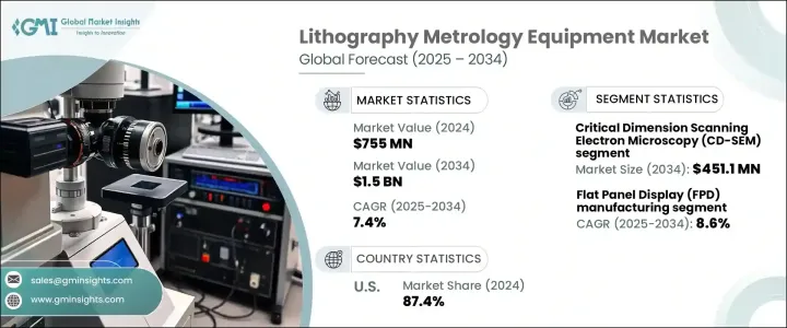
根据技术,市场分为覆盖计量、原子力显微镜 (AFM)、临界尺寸扫描电子显微镜 (CD-SEM)、光学计量和散射测量。其中,CD-SEM 将占据主导地位,预计到 2034 年其市场价值将达到 4.511 亿美元。该技术可确保在检查掩模图案、光刻结构和复杂设计时具有无与伦比的精度,从而实现高度小型化和复杂的半导体生产。对下一代晶片日益增长的需求推动了 CD-SEM 技术的进步,重点是实现更高的分辨率、更高的吞吐量和增强的自动化以满足行业标准。
| 市场范围 | |
|---|---|
| 起始年份 | 2024 |
| 预测年份 | 2025-2034 |
| 起始值 | 7.55亿美元 |
| 预测值 | 15亿美元 |
| 复合年增长率 | 7.4% |
市场根据应用进一步分类,包括 LED 製造、半导体製造、平板显示器 (FPD) 製造、MEMS(微机电系统)等。 FPD 製造业预计将经历最高的成长,2025 年至 2034 年的复合年增长率为 8.6%。这些工具在测量层厚度、对准和分辨率方面发挥关键作用,确保最佳的显示性能和质量,这对于保持电子市场的竞争优势至关重要。
在美国,光刻计量设备市场在 2024 年占据了 87.4% 的份额。对包括 5nm 及更高技术节点在内的尖端节点的投资正在加速 EUV 光刻和先进计量解决方案的采用。此外,对 3D 封装技术的日益关注以及人工智慧、物联网和 5G 的广泛应用,进一步推动了美国对创新和精密光刻计量设备的需求。
目录
第 1 章:方法论与范围
- 市场范围和定义
- 基础估算与计算
- 预测计算
- 资料来源
- 基本的
- 次要
- 付费来源
- 公共资源
第 2 章:执行摘要
第 3 章:产业洞察
- 产业生态系统分析
- 影响价值链的因素
- 利润率分析
- 中断
- 未来展望
- 製造商
- 经销商
- 供应商概况
- 利润率分析
- 重要新闻及倡议
- 监管格局
- 衝击力
- 成长动力
- 半导体技术的进步
- 消费性电子产品需求不断成长
- 5G 和人工智慧 (AI) 应用的成长
- 越来越关注代工和内存製造
- 光学和非光学计量技术进步
- 产业陷阱与挑战
- 先进计量设备成本高昂
- 测量先进节点的复杂性
- 成长动力
- 成长潜力分析
- 波特的分析
- PESTEL 分析
第四章:竞争格局
- 介绍
- 公司市占率分析
- 竞争定位矩阵
- 战略展望矩阵
第 5 章:市场估计与预测:按技术,2021 年至 2034 年
- 主要趋势
- 光学计量
- 临界尺寸扫描电子显微镜 (CD-SEM)
- 迭层测量
- 原子力显微镜 (AFM)
- 散射测量
第 6 章:市场估计与预测:按产品,2021-2034 年
- 主要趋势
- 化学控制设备
- 瓦斯控制设备
- 其他的
第 7 章:市场估计与预测:按工艺,2021 年至 2034 年
- 主要趋势
- 边缘
- 云
第 8 章:市场估计与预测:按应用,2021 年至 2034 年
- 主要趋势
- 半导体製造
- 平面显示器(FPD)製造
- MEMS(微机电系统)
- LED 製造
- 其他的
第 9 章:市场估计与预测:按最终用途产业,2021 年至 2034 年
- 主要趋势
- 整合设备製造商 (IDM)
- 铸造厂
第 10 章:市场估计与预测:按地区,2021 年至 2034 年
- 主要趋势
- 北美洲
- 我们
- 加拿大
- 欧洲
- 英国
- 德国
- 法国
- 义大利
- 西班牙
- 俄罗斯
- 亚太地区
- 中国
- 印度
- 日本
- 韩国
- 澳洲
- 拉丁美洲
- 巴西
- 墨西哥
- 中东及非洲
- 南非
- 沙乌地阿拉伯
- 阿联酋
第 11 章:公司简介
- ASML Holding NV
- Advantest Corporation
- Applied Materials Inc
- Canon Inc.
- Carl Zeiss SMT
- EV Group
- Hitachi High-Tech Corporation
- Holon co Ltd.
- KLA Corporation
- KLA-Tencor
- LAM Research
- Nikon Corporation
- Nova Measuring Instruments Ltd.
- Onto innovation
- Thermo Fisher Scientific Inc.
The Global Lithography Metrology Equipment Market reached USD 755 million in 2024 and is poised to grow at an impressive CAGR of 7.4% between 2025 and 2034. This growth is primarily driven by the surging demand for advanced consumer electronics such as smartphones, tablets, and wearables, which continue to dominate the global market. These devices rely on compact, high-performance integrated circuits (ICs), placing a premium on cutting-edge lithography processes. These advanced techniques are critical for achieving higher chip densities, which are necessary to deliver the next-generation capabilities demanded by consumers and industries alike. Additionally, the rising focus on innovations in semiconductor fabrication, 5G technology adoption, and AI applications is fueling the need for precision metrology solutions. Manufacturers are increasingly investing in state-of-the-art equipment to meet the evolving demands of industries that prioritize accuracy and efficiency in production processes.
By technology, the market is segmented into overlay metrology, Atomic Force Microscopy (AFM), Critical Dimension Scanning Electron Microscopy (CD-SEM), optical metrology, and scatterometry. Among these, CD-SEM is set to dominate, with its market value expected to reach USD 451.1 million by 2034. The unparalleled precision of CD-SEM in measuring nanoscale dimensions makes it indispensable for semiconductor fabrication. This technology ensures unmatched accuracy during the inspection of mask patterns, lithography structures, and intricate designs, enabling the production of highly miniaturized and complex semiconductors. The growing demand for next-generation chips is pushing advancements in CD-SEM technology, with a strong focus on achieving higher resolution, increased throughput, and enhanced automation to meet industry standards.
| Market Scope | |
|---|---|
| Start Year | 2024 |
| Forecast Year | 2025-2034 |
| Start Value | $755 Million |
| Forecast Value | $1.5 Billion |
| CAGR | 7.4% |
The market is further categorized based on applications, which include LED manufacturing, semiconductor manufacturing, Flat Panel Display (FPD) manufacturing, MEMS (Micro-Electro-Mechanical Systems), and others. FPD manufacturing is projected to experience the highest growth, with a CAGR of 8.6% from 2025 to 2034. The rising adoption of larger, high-resolution displays and cutting-edge OLED and microLED technologies has significantly amplified the demand for precise metrology tools. These tools play a pivotal role in measuring layer thickness, alignment, and resolution, ensuring optimal display performance and quality, which are crucial for maintaining a competitive edge in the electronics market.
In the United States, the lithography metrology equipment market accounted for a substantial 87.4% share in 2024. The country's dominance stems from its advanced semiconductor manufacturing capabilities and strong R&D infrastructure. Investments in cutting-edge nodes, including 5nm and beyond, are accelerating the adoption of EUV lithography and advanced metrology solutions. Additionally, the growing focus on 3D packaging technologies and the widespread implementation of AI, IoT, and 5G are further driving the demand for innovative and precise lithography metrology equipment in the United States.
Table of Contents
Chapter 1 Methodology & Scope
- 1.1 Market scope & definitions
- 1.2 Base estimates & calculations
- 1.3 Forecast calculations
- 1.4 Data sources
- 1.4.1 Primary
- 1.4.2 Secondary
- 1.4.2.1 Paid sources
- 1.4.2.2 Public sources
Chapter 2 Executive Summary
- 2.1 Industry synopsis, 2021-2034
Chapter 3 Industry Insights
- 3.1 Industry ecosystem analysis
- 3.1.1 Factor affecting the value chain
- 3.1.2 Profit margin analysis
- 3.1.3 Disruptions
- 3.1.4 Future outlook
- 3.1.5 Manufacturers
- 3.1.6 Distributors
- 3.2 Supplier landscape
- 3.3 Profit margin analysis
- 3.4 Key news & initiatives
- 3.5 Regulatory landscape
- 3.6 Impact forces
- 3.6.1 Growth drivers
- 3.6.1.1 Advancements in semiconductor technology
- 3.6.1.2 Rising demand for consumer electronics
- 3.6.1.3 Growth in 5G and artificial intelligence (AI) applications
- 3.6.1.4 Increasing focus on foundry and memory manufacturing
- 3.6.1.5 Technological advancements in optical and non-optical metrology
- 3.6.2 Industry pitfalls & challenges
- 3.6.2.1 High cost of advanced metrology equipment
- 3.6.2.2 Complexity in measuring advanced nodes
- 3.6.1 Growth drivers
- 3.7 Growth potential analysis
- 3.8 Porter's analysis
- 3.9 PESTEL analysis
Chapter 4 Competitive Landscape, 2024
- 4.1 Introduction
- 4.2 Company market share analysis
- 4.3 Competitive positioning matrix
- 4.4 Strategic outlook matrix
Chapter 5 Market Estimates & Forecast, By Technology, 2021-2034 (USD Million) (Million Units)
- 5.1 Key trends
- 5.2 Optical metrology
- 5.3 Critical dimension scanning electron microscopy (CD-SEM)
- 5.4 Overlay metrology
- 5.5 Atomic force microscopy (AFM)
- 5.6 Scatterometry
Chapter 6 Market Estimates & Forecast, By Product, 2021-2034 (USD Million) (Million Units)
- 6.1 Key trends
- 6.2 Chemical control equipment
- 6.3 Gas control equipment
- 6.4 Others
Chapter 7 Market Estimates & Forecast, By Process, 2021-2034 (USD Million) (Million Units)
- 7.1 Key trends
- 7.2 Edge
- 7.3 Cloud
Chapter 8 Market Estimates & Forecast, By Application, 2021-2034 (USD Million) (Million Units)
- 8.1 Key trends
- 8.2 Semiconductor manufacturing
- 8.3 Flat panel display (FPD) manufacturing
- 8.4 MEMS (micro-electro-mechanical systems)
- 8.5 LED manufacturing
- 8.6 Others
Chapter 9 Market Estimates & Forecast, By End Use Industry, 2021-2034 (USD Million) (Million Units)
- 9.1 Key trends
- 9.2 Integrated Device Manufacturers (IDMs)
- 9.3 Foundries
Chapter 10 Market Estimates & Forecast, By Region, 2021-2034 (USD Million) (Million Units)
- 10.1 Key trends
- 10.2 North America
- 10.2.1 U.S.
- 10.2.2 Canada
- 10.3 Europe
- 10.3.1 UK
- 10.3.2 Germany
- 10.3.3 France
- 10.3.4 Italy
- 10.3.5 Spain
- 10.3.6 Russia
- 10.4 Asia Pacific
- 10.4.1 China
- 10.4.2 India
- 10.4.3 Japan
- 10.4.4 South Korea
- 10.4.5 Australia
- 10.5 Latin America
- 10.5.1 Brazil
- 10.5.2 Mexico
- 10.6 MEA
- 10.6.1 South Africa
- 10.6.2 Saudi Arabia
- 10.6.3 UAE
Chapter 11 Company Profiles
- 11.1 ASML Holding NV
- 11.2 Advantest Corporation
- 11.3 Applied Materials Inc
- 11.4 Canon Inc.
- 11.5 Carl Zeiss SMT
- 11.6 EV Group
- 11.7 Hitachi High-Tech Corporation
- 11.8 Holon co Ltd.
- 11.9 KLA Corporation
- 11.10 KLA-Tencor
- 11.11 LAM Research
- 11.12 Nikon Corporation
- 11.13 Nova Measuring Instruments Ltd.
- 11.14 Onto innovation
- 11.15 Thermo Fisher Scientific Inc.
 半导体微影术曝光设备:全球市占率及排名、总收入及需求预测(2026-2032年)
 微影术测量设备市场:依设备类型、技术、波长和应用划分-2026-2032年全球市场预测
 半导体步进系统市场分析与预测(至2035年):类型、产品类型、服务、技术、组件、应用、最终用户、製程、功能、设备
 半导体微影术设备:市场占有率分析、产业趋势与统计、成长预测(2026-2031)
 2026年全球半导体微影术设备市场报告
 微影术计量设备市场规模、份额和成长分析(按设备类型、技术、应用、最终用户产业、自动化程度和地区划分)-产业预测,2026-2033年
 模板微影术市场报告:2030 年趋势、预测与竞争分析