


 |
市场调查报告书
商品编码
1940697
半导体微影术设备:市场占有率分析、产业趋势与统计、成长预测(2026-2031)Semiconductor Lithography Equipment - Market Share Analysis, Industry Trends & Statistics, Growth Forecasts (2026 - 2031) |
||||||
※ 本网页内容可能与最新版本有所差异。详细情况请与我们联繫。
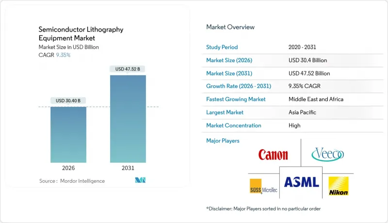
预计半导体微影术设备市场将从 2025 年的 278 亿美元成长到 2026 年的 304 亿美元,到 2031 年达到 475.2 亿美元,2026 年至 2031 年的复合年增长率为 9.35%。
这一成长势头主要得益于向极紫外线 (EUV) 光刻技术的转型以及即将推出的高数值孔径 (高NA) EUV 平台、人工智慧伺服器的普及以及需要更高密度图形化精度的万亿晶体管图形加速器的出现。亚太地区仍是製造业产能扩张的关键驱动力,这主要得益于台湾晶圆代工的优势以及韩国高达 4,710 亿美元的超级产业丛集计画。虽然深紫外线 (DUV) 设备作为成熟製程节点的基础仍然至关重要,但高数值孔径 EUV 设备的订单量表明,整个生态系统正在迅速转型为 1 奈米以下製程。儘管资本投资强度和出口限制仍然是推广应用的主要障碍,但政府补贴、封装创新和节能设备设计正在共同推动先进曝光系统的应用范围不断扩大。
全球半导体微影术设备市场趋势与洞察
小型化製程推动了EUV技术的应用
电晶体密度的不断提高推动了对7奈米以下微缩製程的需求,而这只有极紫外光刻(EUV)才能实现。台积电在其新竹工厂成功实现了高数值孔径(NA)光刻机的首次光刻,为2030年实现1奈米製程的量产做准备。 ASML的EXE平台采用变形光学元件实现了8奈米分辨率,与先前的NXE型号相比,影像对比度提高了40%。调查团队已实现了5奈米线间距的干涉曝光,证实了其性能远低于蓝图。预计伺服器级处理器的电晶体数量将翻一番,达到2000亿个,这将进一步推高光刻产能的需求。这些里程碑事件凸显了埃级微缩製程的快速发展,并将高数值孔径光刻机确立为最重要的资本投资项目。
人工智慧和资料中心对尖端晶片的需求
人工智慧伺服器需要拥有超过2兆个电晶体的多晶片GPU。预计到2030年,半导体销售额将超过1兆美元,其中人工智慧加速器和高频宽记忆体将成为关键的成长引擎。诸如CoWoS等先进封装技术对线路重布的微影术套刻精度提出了更高的要求。三星的异质整合蓝图和台积电的CoWoS产能扩张正在推动大尺寸曝光设备的紧急征兆。阿布达比拥有1-5GW人工智慧运算丛集,配备数十万个GPU,标誌着一个新地区进入了资本支出週期。
EUV曝光设备需要极高的资本投入
ASML的高数值孔径(高NA)光刻机每台造价高达3.8亿美元,是早期EUV平台价格的两倍。洁净室改造、隔振以及兆瓦级的电力和冷却设备进一步增加了总拥有成本。预计到2025年底,全球将安装不到20台高NA光刻机,中型晶圆厂将无缘参与这场埃级光刻竞赛。冲绳科学技术大学院大学(OIST)的一项研究提案了双镜投影机和20瓦光源的方案,该方案有望将电力消耗降低90%,从而可能减轻未来的资本支出。
细分市场分析
到2025年,DUV平台将维持56.10%的半导体微影术设备市场份额,凸显了其在成熟节点和成本敏感型生产线上的重要性。高数值孔径EUV目前在半导体微影术设备市场中所占份额较小,但预计到2031年将以10.54%的复合年增长率增长,届时单次曝光1nm成像将成为量产现实。 ASML EXE系列中的0.55 NA变形投影技术提高了景深,实现了以往无需四重图形化即可达到的缺陷密度目标。 Imec在20nm间距金属线上实现了90%的电气产量比率,证实了其已做好量产准备。
传统极紫外光刻技术对于5nm逻辑晶片、 NAND快闪记忆体和DRAM更新仍然至关重要,0.33数值孔径(NA)可提供可接受的套刻精度,并支援多重图形化。深紫外线浸没式微影技术已在许多晶圆厂实现成本摊销,在类比、射频和MEMS製程中仍保持着晶粒优势。Canon的奈米压印试验线和尼康的浸没式光刻技术改进表明,在细分市场存在竞争,但ASML对以光罩格式为中心的生态系统的依赖,巩固了其平台优势。
区域分析
亚太地区预计到2025年将占67.60%的市场份额,这反映了逻辑和记忆体超大型晶圆厂集中在台湾、韩国、日本和中国当地。韩国价值4,710亿美元的丛集正在增加多台极紫外光刻机,而日本政府的支持也促使台积电在熊本建设第二座晶圆厂。儘管受到出口限制,但随着国内光刻计划的扩张,中国在2024年仍将在晶圆厂设备方面投入490亿美元。
北美位居第二,在《晶片技术创新法案》(CHIPS Act)的联合资助下,英特尔、台积电和三星在美国的计划投资额超过2,000亿美元。光是亚利桑那州的双晶圆厂园区在预测期内就将安装超过25台极紫外光刻设备。奥勒冈、俄亥俄州和德克萨斯的晶圆厂丛集将扩大地理冗余度,从而增强该地区对设备服务的需求。
中东和非洲地区虽然目前规模较小,但年复合成长率高达12.48%。沙乌地阿拉伯10亿沙特里亚尔的创投基金正在支持建造国家半导体中心,而阿联酋的资料中心计划也需要在地化的先进封装技术。政府间的技术转移协议有助于加快专案进度,但劳动力和供应链深度仍是发展的瓶颈。
其他福利:
- Excel格式的市场预测(ME)表
- 3个月的分析师支持
目录
第一章 引言
- 研究假设和市场定义
- 调查范围
第二章调查方法
第三章执行摘要
第四章 市场情势
- 市场概览
- 市场驱动因素
- 製程节点尺寸缩小推动了EUV技术的应用
- 人工智慧和资料中心对尖端晶片的需求
- 政府晶圆厂补贴(例如,晶片法案)
- 先进封装(2.5D/3D IC)的快速成长
- 高数值孔径 EUV 光刻更新率加快设备週期
- 化合物半导体光刻需求
- 市场限制
- EUV扫描器的资本投资极为昂贵
- 子系统供应链瓶颈
- 永续性和能源利用面临的压力
- 对华出口管制条例
- 价值链分析
- 监管环境
- 技术展望
- 波特五力分析
- 新进入者的威胁
- 供应商的议价能力
- 买方的议价能力
- 替代品的威胁
- 竞争对手之间的竞争
- 定价分析
- 宏观经济因素的影响
第五章 市场规模与成长预测
- 透过印刷方法
- 深紫外线(DUV)
- 极紫外线(EUV)
- 高数值孔径极紫外光刻
- 透过使用
- 先进包装
- MEMS元件
- LED元件
- 功率半导体和化合物半导体
- 最终用户
- 专业铸造厂
- 整合装置製造商(IDM)
- 半导体外包组装和测试服务 (OSAT)
- 按地区
- 北美洲
- 我们
- 加拿大
- 墨西哥
- 南美洲
- 巴西
- 阿根廷
- 南美洲其他地区
- 欧洲
- 德国
- 英国
- 法国
- 义大利
- 西班牙
- 俄罗斯
- 其他欧洲地区
- 亚太地区
- 中国
- 日本
- 印度
- 韩国
- 东南亚
- 亚太其他地区
- 中东和非洲
- 中东
- 沙乌地阿拉伯
- 阿拉伯聯合大公国
- 土耳其
- 其他中东地区
- 非洲
- 南非
- 奈及利亚
- 其他非洲地区
- 中东
- 北美洲
第六章 竞争情势
- 市场集中度
- 策略趋势
- 市占率分析
- 公司简介
- ASML Holding NV
- Nikon Corporation
- Canon Inc.
- Shanghai Micro Electronics Equipment(Group)Co., Ltd.
- SUSS MicroTec SE
- EV Group
- Veeco Instruments Inc.
- Onto Innovation Inc.
- JEOL Ltd.
- Neutronix Quintel Inc.
- Mycronic AB
- NuFlare Technology Inc.
- Ushio Inc.
- Ultratech(Veeco)
- Mapper Lithography BV
- Visitech AS
- KLA Corporation
- MKS Instruments(Newport)
- Inpria Corp.
- Tamarack Scientific Co.
第七章 市场机会与未来展望
The semiconductor lithography equipment market is expected to grow from USD 27.8 billion in 2025 to USD 30.4 billion in 2026 and is forecast to reach USD 47.52 billion by 2031 at 9.35% CAGR over 2026-2031.
Momentum stems from the shift toward extreme ultraviolet (EUV) and forthcoming High-NA EUV platforms, the surge in artificial-intelligence servers, and multi-trillion-transistor graphics accelerators that demand denser patterning precision. Asia-Pacific remains the fulcrum of manufacturing capacity expansions, led by Taiwan's foundry dominance and South Korea's USD 471 billion mega-cluster program. Deep-ultraviolet (DUV) tools still anchor mature nodes, but the pipeline of High-NA EUV orders shows how quickly the ecosystem is pivoting toward sub-1 nm production. Capital-expenditure intensity and export-control compliance are the main brakes on diffusion, yet government subsidies, packaging innovations, and energy-efficient tool designs together widen the addressable base for advanced exposure systems.
Global Semiconductor Lithography Equipment Market Trends and Insights
Shrinking Process Nodes Drive EUV Adoption
Growing transistor density forces sub-7 nm geometries that only EUV can achieve. TSMC recorded first light on a High-NA tool in Hsinchu as it prepares 1 nm mass output by 2030. ASML's EXE platform reaches 8 nm resolution with anamorphic optics, a 40% imaging-contrast jump over prior NXE models. Research teams demonstrated 5 nm line-space interference printing, confirming far-below-roadmap capability. Server-class processors are projected to double to 200 billion transistors, magnifying lithography throughput needs. These milestones underline a rapid cadence toward angstrom dimensions that places High-NA tools at the center of capex priorities.
AI and Data-Center Demand for Leading-Edge Chips
Artificial-intelligence servers require multi-chiplet GPUs pushing past 2 trillion transistors. Semiconductor revenue is modeled to top USD 1 trillion by 2030, with AI accelerators and high-bandwidth memory as primary growth engines. Advanced packaging formats such as CoWoS intensify lithography overlay accuracy for redistribution layers. Samsung's heterogeneous-integration roadmap and TSMC's CoWoS capacity ramp have driven rush orders for large-panel exposure tools. Abu Dhabi's 1-5 GW AI compute cluster, featuring hundreds of thousands of GPUs, signals new geographies entering the capex cycle.
Ultra-High Capex of EUV Scanners
ASML's High-NA units list at USD 380 million each, double the cost of early EUV platforms. Total cost of ownership multiplies after clean-room reconfiguration, vibration isolation, and megawatt-class power-and-cooling utilities. Fewer than 20 High-NA machines are likely installed worldwide by end-2025, leaving mid-tier fabs locked out of the angstrom race. Research at the Okinawa Institute proposes a two-mirror projector and a 20-W source that could shrink power draw by 90%, hinting at future capex relief.
Other drivers and restraints analyzed in the detailed report include:
- Government Fab Subsidies Drive Equipment Investment
- Advanced-Packaging Boom Accelerates Equipment Demand
- Export-Control Restrictions to China
For complete list of drivers and restraints, kindly check the Table Of Contents.
Segment Analysis
In 2025, DUV platforms maintained 56.10% semiconductor lithography equipment market share, underlining their role in mature-node and cost-sensitive lines. High-NA EUV, although a smaller slice of the semiconductor lithography equipment market size today, is forecast to grow 10.54% CAGR through 2031 as single-exposure 1 nm imaging becomes a production reality. The 0.55 NA anamorphic projection inside ASML's EXE series improves depth-of-focus, enabling defect-density targets previously unattainable without quadruple patterning. Imec's 90% electrical yield on 20 nm pitch metal lines corroborates readiness for volume runs.
Conventional EUV remains indispensable for 5 nm logic, NAND flash, and DRAM refreshes, where 0.33 NA offers acceptable overlay with multi-patterning. Deep-UV immersion, already fully depreciated at many fabs, keeps the cost-per-die edge for analog, RF, and MEMS flows. Canon's nano-imprint pilot lines and Nikon's immersion enhancements signal niche competitive threats, yet ecosystem lock-in around ASML reticle formats sustains its platform moat.
The Semiconductor Lithography Machine Manufacturers Market is Segmented by Type (Deep Ultraviolet Lithography and Extreme Ultraviolet Lithography), Application (Advanced Packaging, MEMS Devices, and LED Devices), and Geography (North America, Europe, and More). The Market Forecasts are Provided in Terms of Value (USD).
Geography Analysis
Asia-Pacific's 67.60% share in 2025 reflects the agglomeration of logic and memory megafabs across Taiwan, South Korea, Japan, and mainland China. South Korea's USD 471 billion cluster will add multiple EUV suites, while Japan's government incentives lure TSMC into second-phase Kumamoto construction. China, despite export curbs, still spent USD 49 billion on overall fab tools in 2024 as domestic lithography projects scale.
North America ranks second, fueled by CHIPS Act co-funding that pushes combined Intel, TSMC, and Samsung U.S. projects past USD 200 billion. Arizona's twin-fab campus alone will deploy more than 25 EUV scanners over the forecast horizon. Fab clusters in Oregon, Ohio, and Texas broaden geographic redundancy and strengthen regional tool-service demand.
The Middle East and Africa, though small today, show a 12.48% CAGR. Saudi Arabia's SAR 1 billion venture fund underpins the National Semiconductor Hub, while UAE data-center projects necessitate local advanced-packaging capacity. Government-to-government technology-transfer accords expedite timeline compression, but workforce and supply-chain depth remain developmental bottlenecks.
- ASML Holding N.V.
- Nikon Corporation
- Canon Inc.
- Shanghai Micro Electronics Equipment (Group) Co., Ltd.
- SUSS MicroTec SE
- EV Group
- Veeco Instruments Inc.
- Onto Innovation Inc.
- JEOL Ltd.
- Neutronix Quintel Inc.
- Mycronic AB
- NuFlare Technology Inc.
- Ushio Inc.
- Ultratech (Veeco)
- Mapper Lithography B.V.
- Visitech AS
- KLA Corporation
- MKS Instruments (Newport)
- Inpria Corp.
- Tamarack Scientific Co.
Additional Benefits:
- The market estimate (ME) sheet in Excel format
- 3 months of analyst support
TABLE OF CONTENTS
1 INTRODUCTION
- 1.1 Study Assumptions and Market Definition
- 1.2 Scope of the Study
2 RESEARCH METHODOLOGY
3 EXECUTIVE SUMMARY
4 MARKET LANDSCAPE
- 4.1 Market Overview
- 4.2 Market Drivers
- 4.2.1 Shrinking process nodes drive EUV adoption
- 4.2.2 AI and data-center demand for leading-edge chips
- 4.2.3 Government fab subsidies (e.g., CHIPS Act)
- 4.2.4 Advanced-packaging boom (2.5D/3D IC)
- 4.2.5 High-NA EUV refresh accelerates tool cycles
- 4.2.6 Compound-semiconductor lithography demand
- 4.3 Market Restraints
- 4.3.1 Ultra-high capex of EUV scanners
- 4.3.2 Sub-system supply-chain bottlenecks
- 4.3.3 Sustainability and energy-use pressures
- 4.3.4 Export-control restrictions to China
- 4.4 Value Chain Analysis
- 4.5 Regulatory Landscape
- 4.6 Technological Outlook
- 4.7 Porter's Five Forces Analysis
- 4.7.1 Threat of New Entrants
- 4.7.2 Bargaining Power of Suppliers
- 4.7.3 Bargaining Power of Buyers
- 4.7.4 Threat of Substitutes
- 4.7.5 Competitive Rivalry
- 4.8 Pricing Analysis
- 4.9 Impact of Macroeconomic Factors
5 MARKET SIZE AND GROWTH FORECASTS (VALUE)
- 5.1 By Lithography Type
- 5.1.1 Deep Ultraviolet (DUV)
- 5.1.2 Extreme Ultraviolet (EUV)
- 5.1.3 High-NA EUV
- 5.2 By Application
- 5.2.1 Advanced Packaging
- 5.2.2 MEMS Devices
- 5.2.3 LED Devices
- 5.2.4 Power and Compound Semiconductors
- 5.3 By End-User
- 5.3.1 Pure-play Foundries
- 5.3.2 Integrated Device Manufacturers (IDMs)
- 5.3.3 Outsourced Semiconductor Assembly and Test (OSAT)
- 5.4 By Geography
- 5.4.1 North America
- 5.4.1.1 United States
- 5.4.1.2 Canada
- 5.4.1.3 Mexico
- 5.4.2 South America
- 5.4.2.1 Brazil
- 5.4.2.2 Argentina
- 5.4.2.3 Rest of South America
- 5.4.3 Europe
- 5.4.3.1 Germany
- 5.4.3.2 United Kingdom
- 5.4.3.3 France
- 5.4.3.4 Italy
- 5.4.3.5 Spain
- 5.4.3.6 Russia
- 5.4.3.7 Rest of Europe
- 5.4.4 Asia Pacific
- 5.4.4.1 China
- 5.4.4.2 Japan
- 5.4.4.3 India
- 5.4.4.4 South Korea
- 5.4.4.5 South East Asia
- 5.4.4.6 Rest of Asia Pacific
- 5.4.5 Middle East and Africa
- 5.4.5.1 Middle East
- 5.4.5.1.1 Saudi Arabia
- 5.4.5.1.2 United Arab Emirates
- 5.4.5.1.3 Turkey
- 5.4.5.1.4 Rest of Middle East
- 5.4.5.2 Africa
- 5.4.5.2.1 South Africa
- 5.4.5.2.2 Nigeria
- 5.4.5.2.3 Rest of Africa
- 5.4.5.1 Middle East
- 5.4.1 North America
6 COMPETITIVE LANDSCAPE
- 6.1 Market Concentration
- 6.2 Strategic Moves
- 6.3 Market Share Analysis
- 6.4 Company Profiles (includes Global level Overview, Market level overview, Core Segments, Financials as available, Strategic Information, Market Rank/Share for key companies, Products and Services, and Recent Developments)
- 6.4.1 ASML Holding N.V.
- 6.4.2 Nikon Corporation
- 6.4.3 Canon Inc.
- 6.4.4 Shanghai Micro Electronics Equipment (Group) Co., Ltd.
- 6.4.5 SUSS MicroTec SE
- 6.4.6 EV Group
- 6.4.7 Veeco Instruments Inc.
- 6.4.8 Onto Innovation Inc.
- 6.4.9 JEOL Ltd.
- 6.4.10 Neutronix Quintel Inc.
- 6.4.11 Mycronic AB
- 6.4.12 NuFlare Technology Inc.
- 6.4.13 Ushio Inc.
- 6.4.14 Ultratech (Veeco)
- 6.4.15 Mapper Lithography B.V.
- 6.4.16 Visitech AS
- 6.4.17 KLA Corporation
- 6.4.18 MKS Instruments (Newport)
- 6.4.19 Inpria Corp.
- 6.4.20 Tamarack Scientific Co.
7 MARKET OPPORTUNITIES AND FUTURE OUTLOOK
- 7.1 White-space and Unmet-Need Assessment


