


 |
市场调查报告书
商品编码
1699355
光刻设备市场机会、成长动力、产业趋势分析及2025-2034年预测Lithography Equipment Market Opportunity, Growth Drivers, Industry Trend Analysis, and Forecast 2025-2034 |
||||||
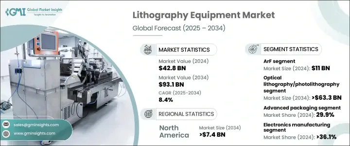
2024 年全球光刻设备市场价值为 428 亿美元,预计 2025 年至 2034 年的复合年增长率为 8.4%。这一增长是由对先进和紧凑半导体元件的需求激增所推动的,尤其是在消费性电子产品领域。随着现代电子设备的不断发展,製造商正在突破半导体设计的界限,以提高处理能力、能源效率和整体性能。这种日益增长的复杂性推动了尖端光刻技术的采用,确保了具有卓越功能的高密度晶片的生产。
半导体产业的晶片製造流程正在快速进步,光刻设备在下一代设备中发挥着至关重要的作用。人工智慧、物联网 (IoT) 和 5G 技术的日益融合,进一步扩大了对高效能晶片的需求,对先进的光刻解决方案产生了强劲的需求。此外,半导体产业的竞争性质导致光刻技术不断创新,使製造商能够在半导体製造中实现更高的精度和效率。随着半导体产业朝向更复杂的架构发展,对光刻设备的依赖不断扩大,使其成为技术进步的关键驱动力。
| 市场范围 | |
|---|---|
| 起始年份 | 2024 |
| 预测年份 | 2025-2034 |
| 起始值 | 428亿美元 |
| 预测值 | 931亿美元 |
| 复合年增长率 | 8.4% |
市场按技术细分为 ArF、KrF、i-line、ArF 浸没式和极紫外线 (EUV) 微影。其中,ArF 领域在 2024 年的价值为 110 亿美元,并将实现显着增长,特别是由于其在视讯串流、线上游戏以及虚拟和扩增实境等快速成长的行业中的应用。 ArF 技术在深紫外线 (DUV) 微影领域提供了增强的性能,这对于生产高性能、高密度半导体装置至关重要。随着对强大而高效的晶片的需求不断增加,ArF 领域预计将进一步扩大,并加强其在推动半导体创新方面的作用。
光刻设备进一步按类型分类,包括光学微影、电子束微影、光罩对准器、离子光刻、X射线微影和奈米压印微影。其中,光学光刻技术(也称为照相平版印刷技术)仍然占据主导地位,预计到 2034 年将达到 633 亿美元。其广泛采用归因于它可以无缝整合到现有的半导体生产设施中,使其成为晶片製造商具有成本效益且可扩展的解决方案。随着解析度和效率的不断提高,光学光刻技术仍然是半导体製造的首选,确保了其在未来几年的强大市场地位。
北美光刻设备市场将大幅成长,预计到 2034 年将达到 74 亿美元。这一成长是由汽车、消费性电子和资料中心等产业对半导体的需求不断增长所推动的。加强供应链弹性和将半导体製造带回国内的努力正在进一步推动市场扩张。此外,北美对研发的重视,加上高技能劳动力,正在加速光刻技术的创新,使该地区成为半导体进步的关键枢纽。
目录
第一章:方法论与范围
第二章:执行摘要
第三章:行业洞察
- 产业生态系统分析
- 产业衝击力
- 成长动力
- 消费性电子产品对先进、微型半导体元件的需求不断增长
- 光刻工艺的技术进步
- 汽车电气化需求不断增长,电动车在全球普及
- 全球物联网和人工智慧技术日益流行
- 对紧凑型和节能设备的需求不断增长
- 产业陷阱与挑战
- 生产成本高
- 安全问题
- 成长动力
- 成长潜力分析
- 监管格局
- 技术格局
- 未来市场趋势
- 差距分析
- 波特的分析
- PESTEL分析
第四章:竞争格局
- 介绍
- 公司市占率分析
- 主要市场参与者的竞争分析
- 竞争定位矩阵
- 策略仪表板
第五章:市场估计与预测:按技术,2021 年至 2034 年
- 主要趋势
- 氩氟
- 氪氟
- i线
- Arf 浸入式
- 极紫外线 (EUV) 微影
第六章:市场估计与预测:按设备,2021 年至 2034 年
- 主要趋势
- 光学光刻/光刻
- 掩模对准器
- 电子束光刻
- 离子光刻
- X射线光刻
- 奈米压印光刻
第七章:市场估计与预测:按应用,2021 年至 2034 年
- 主要趋势
- 先进封装
- MEMS 设备
- LED 设备
- 其他的
第八章:市场估计与预测:依最终用途,2021 年至 2034 年
- 主要趋势
- 电子製造业
- 医疗保健和生命科学
- 汽车产业
- 电信
- 其他的
第九章:市场估计与预测:按地区,2021 年至 2034 年
- 主要趋势
- 北美洲
- 我们
- 加拿大
- 欧洲
- 英国
- 德国
- 法国
- 义大利
- 西班牙
- 亚太地区
- 中国
- 日本
- 印度
- 韩国
- 澳新银行
- 台湾
- 拉丁美洲
- 巴西
- 墨西哥
- 中东和非洲
- 沙乌地阿拉伯
- 阿联酋
- 以色列
- 南非
第十章:公司简介
- ASML Holding NV
- Nikon Corporation
- Canon Inc.
- Veeco Instruments Inc.
- SUSS MicroTec AG
- EV Group
- SCREEN Holdings Co., Ltd.
- Onto Innovation Inc.
- JEOL Ltd
- Neutronix Quintel Inc. (NXQ)
- Advantest
- Shanghai Micro Electronics Equipment (Group) Co., Ltd.
The Global Lithography Equipment Market was valued at USD 42.8 billion in 2024 and is projected to grow at a CAGR of 8.4% from 2025 to 2034. This growth is fueled by the surging demand for advanced and compact semiconductor components, particularly in consumer electronics. As modern electronic devices continue to evolve, manufacturers are pushing the boundaries of semiconductor design to enhance processing power, energy efficiency, and overall performance. This growing complexity is driving the adoption of cutting-edge lithography technologies, ensuring the production of high-density chips with superior functionality.
The semiconductor industry is experiencing rapid advancements in chip manufacturing processes, with lithography equipment playing a crucial role in enabling next-generation devices. The increasing integration of artificial intelligence, the Internet of Things (IoT), and 5G technology is further amplifying the need for high-performance chips, creating a strong demand for advanced lithography solutions. Moreover, the competitive nature of the semiconductor industry has led to continuous innovation in lithography techniques, allowing manufacturers to achieve higher precision and efficiency in semiconductor fabrication. As the semiconductor industry moves toward more intricate architectures, the reliance on lithography equipment continues to expand, making it a key driver of technological progress.
| Market Scope | |
|---|---|
| Start Year | 2024 |
| Forecast Year | 2025-2034 |
| Start Value | $42.8 Billion |
| Forecast Value | $93.1 Billion |
| CAGR | 8.4% |
The market is segmented by technology into ArF, KrF, i-line, ArF immersion, and Extreme Ultraviolet (EUV) Lithography. Among these, the ArF segment was valued at USD 11 billion in 2024 and is set for significant growth, particularly due to its applications in fast-growing industries like video streaming, online gaming, and virtual and augmented reality. ArF technology delivers enhanced performance within Deep Ultraviolet (DUV) lithography, which is essential for producing high-performance, high-density semiconductor devices. As the need for powerful and efficient chips increases, the ArF segment is expected to expand further, reinforcing its role in driving semiconductor innovation.
Lithography equipment is further categorized by type, including optical lithography, electron beam lithography, mask aligners, ion lithography, X-ray lithography, and nanoimprint lithography. Among these, optical lithography, also known as photolithography, remains the dominant segment and is projected to reach USD 63.3 billion by 2034. Its widespread adoption is attributed to its seamless integration into existing semiconductor production facilities, making it a cost-effective and scalable solution for chipmakers. With continuous advancements improving resolution and efficiency, optical lithography remains a preferred choice for semiconductor manufacturing, ensuring its strong market presence in the years ahead.
North America lithography equipment market is set for substantial growth, projected to reach USD 7.4 billion by 2034. This surge is driven by rising semiconductor demand across industries such as automotive, consumer electronics, and data centers. Efforts to strengthen supply chain resilience and bring semiconductor manufacturing back to domestic regions are further fueling market expansion. Additionally, North America's emphasis on research and development, coupled with a highly skilled workforce, is accelerating innovation in lithography technology, positioning the region as a key hub for semiconductor advancements.
Table of Contents
Chapter 1 Methodology and Scope
- 1.1 Market scope and definitions
- 1.2 Research design
- 1.2.1 Research approach
- 1.2.2 Data collection methods
- 1.3 Base estimates and calculations
- 1.3.1 Base year calculation
- 1.3.2 Key trends for market estimation
- 1.4 Forecast model
- 1.5 Primary research and validation
- 1.5.1 Primary sources
- 1.5.2 Data mining sources
Chapter 2 Executive Summary
- 2.1 Industry 360° synopsis
Chapter 3 Industry Insights
- 3.1 Industry ecosystem analysis
- 3.2 Industry impact forces
- 3.2.1 Growth drivers
- 3.2.1.1 Rising demand for advanced and miniaturized semiconductor components in consumer electronics
- 3.2.1.2 Technological advancements in the lithography process
- 3.2.1.3 Increasing demand for electrification in vehicles and the global proliferation of electric vehicles
- 3.2.1.4 Increasing trend toward IoT and AI technology around the globe
- 3.2.1.5 Growing demand for Compact and Power-Efficient Devices
- 3.2.2 Industry pitfalls and challenges
- 3.2.2.1 High production cost
- 3.2.2.2 Security concerns
- 3.2.1 Growth drivers
- 3.3 Growth potential analysis
- 3.4 Regulatory landscape
- 3.5 Technology landscape
- 3.6 Future market trends
- 3.7 Gap analysis
- 3.8 Porter's analysis
- 3.9 PESTEL analysis
Chapter 4 Competitive Landscape, 2024
- 4.1 Introduction
- 4.2 Company market share analysis
- 4.3 Competitive analysis of major market players
- 4.4 Competitive positioning matrix
- 4.5 Strategy dashboard
Chapter 5 Market Estimates and Forecast, By Technology, 2021 – 2034 (USD Mn)
- 5.1 Key trends
- 5.2 ArF
- 5.3 KrF
- 5.4 i-line
- 5.5 Arf immersion
- 5.6 Extreme Ultraviolet (EUV) Lithography
Chapter 6 Market Estimates and Forecast, By Equipment, 2021 – 2034 (USD Mn)
- 6.1 Key trends
- 6.2 Optical Lithography/Photolithography
- 6.3 Mask aligners
- 6.4 Electron beam lithography
- 6.5 Ion lithography
- 6.6 X-Ray lithography
- 6.7 Nanoimprint lithography
Chapter 7 Market Estimates and Forecast, By Application, 2021 – 2034 (USD Mn)
- 7.1 Key trends
- 7.2 Advanced packaging
- 7.3 MEMS devices
- 7.4 LED devices
- 7.5 Others
Chapter 8 Market Estimates and Forecast, By End Use, 2021 – 2034 (USD Mn)
- 8.1 Key trends
- 8.2 Electronics manufacturing
- 8.3 Healthcare and Life sciences
- 8.4 Automotive industry
- 8.5 Telecommunications
- 8.6 Others
Chapter 9 Market Estimates and Forecast, By Region, 2021 – 2034 (USD Mn)
- 9.1 Key trends
- 9.2 North America
- 9.2.1 U.S.
- 9.2.2 Canada
- 9.3 Europe
- 9.3.1 UK
- 9.3.2 Germany
- 9.3.3 France
- 9.3.4 Italy
- 9.3.5 Spain
- 9.4 Asia Pacific
- 9.4.1 China
- 9.4.2 Japan
- 9.4.3 India
- 9.4.4 South Korea
- 9.4.5 ANZ
- 9.4.6 Taiwan
- 9.5 Latin America
- 9.5.1 Brazil
- 9.5.2 Mexico
- 9.6 Middle East and Africa
- 9.6.1 Saudi Arabia
- 9.6.2 UAE
- 9.6.3 Israel
- 9.6.4 South Africa
Chapter 10 Company Profiles
- 10.1 ASML Holding N.V.
- 10.2 Nikon Corporation
- 10.3 Canon Inc.
- 10.4 Veeco Instruments Inc.
- 10.5 SUSS MicroTec AG
- 10.6 EV Group
- 10.7 SCREEN Holdings Co., Ltd.
- 10.8 Onto Innovation Inc.
- 10.9 JEOL Ltd
- 10.10 Neutronix Quintel Inc. (NXQ)
- 10.11 Advantest
- 10.12 Shanghai Micro Electronics Equipment (Group) Co., Ltd.
 ArFi微影术系统设备市场规模、份额和成长分析:按产品类型、吞吐量、技术、技术节点、应用、最终用户和地区划分 - 2026-2033年产业预测
 微影术设备市场分析及预测(至2035年):依类型、产品、技术、组件、应用、最终用户、製程、安装类型、设备及解决方案划分
 100奈米以下光刻:全球市场分析与策略课题
 按软体类型、最终用户、部署类型和製程节点分類的计算微影术软体市场 - 全球预测 2026-2032
 DUV光刻系统市场:按类型、应用、国家和地区划分 - 全球产业分析、市场规模、市场份额及2025-2032年预测
 面向先进节点的下一代微影术技术:技术与应用光刻设备市场规模、占有率、成长及全球产业分析:依类型、应用和地区划分的洞察与预测(2024-2032 年)
 电子束微影(EBL)-全球市场占有率和排名、总收入和需求预测(2025-2031年)微影术材质:全球市占率及排名、总收入及需求预测(2025-2031年)计算微影术软体:全球市场占有率和排名、总收入和需求预测(2025-2031年)