


 |
市场调查报告书
商品编码
1479763
100奈米以下光刻:全球市场分析与策略课题Sub-100nm Lithography: Market Analysis and Strategic Issues |
||||||
促进因素
随着半导体技术节点的缩小以及对更小、更复杂的半导体装置的需求的增加,多种驱动因素□□正在推动光刻技术的进步,以应对这些课题。
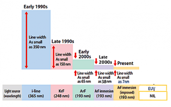
技术扩展:对于每个新技术节点,半导体製造商的目标是缩小电晶体和互连的尺寸,以提高效能、功率效率和密度。 为了实现这种高精度和高解析度的小型化,先进的光刻技术必不可少,并且正在推动下一代光刻工具的开发。
使用EUV微影:EUV微影的波长比传统光学微影更短,因此可以形成更精细、更复杂的图案。 随着节点变得更小,为了实现所需的图案分辨率,采用 EUV 光刻变得越来越必要。
多重图案化技术:随着特征尺寸接近光学微影的极限,SADP、SAQP 和MBML 等多重图案化技术对于实现所需的特征密度和间距变得至关重要。 这些技术需要多次曝光和蚀刻步骤来创建复杂的图案,增加了对先进光刻解决方案的需求。
解析度增强技术(RET):为了提高图案转移的解析度和保真度,光刻工具包括光学邻近校正(OPC)、相移掩模(PSM)、来源整合瞭解析度增强技术例如掩模优化(SMO)。 这些 RET 有助于减轻衍射和其他光学限制的影响,从而能够在先进节点中製造更精细的特征。
提高製程控制和产量:随着特征尺寸的减小,保持严格的製程控製成为越来越大的课题。 先进的光刻工具结合了先进的计量和製程控制功能,以确保均匀性、覆盖精度和减少缺陷。 这些功能对于在先进节点实现高产量和製造一致性至关重要。
新兴应用和市场需求:人工智慧、5G 连接、自动驾驶汽车和物联网设备等新兴技术正在推动对具有特定性能要求的专用半导体设备的需求。 先进的光刻解决方案对于这些应用所需的复杂结构和材料的图案化至关重要,并且正在推动光刻技术的创新。
需要此报告
半导体光刻是半导体製造的基石,也是製造支援现代电子产品的复杂半导体装置的极其重要的製程。 随着半导体技术的进步,光刻技术也在进步,突破瞭解析度、精准度和产量的极限,使得製造更精细、更复杂的半导体结构成为可能。
由于对更高性能和节能电子设备的需求,半导体产业正在表现出对小型化的不懈追求。 极紫外线 (EUV) 微影、多重图案化和浸没式微影等先进微影技术在实现亚 10 奈米尺寸、突破半导体製造能力的极限方面发挥关键作用。
本报告对全球半导体光刻市场进行了全面分析,深入瞭解市场规模、成长动力、竞争格局和新的市场机会。
目录
第一章简介
第 2 章执行摘要
- 主要问题摘要
- 市场机会摘要
第 3 章光刻技术的问题与趋势
- 光学系统
- 简介
- 步进重复对准器
- 深层紫外线 (DUV)
- 极紫外光
- 奈米压印光刻
- X射线光刻
- 电子束光刻
- 离子束光刻
第 4 章使用者与供应商策略
- 确定您的光刻需求
- 供应商基准
- 价格
- 供应商的承诺与态度
- 供应商能力
- 系统功能
- 设备评估期间供应商的回馈
- 设备生产过程中供应商的回馈
- 竞争环境
- 1级无尘室设备
- 未来工厂的设备
- 机会
第五章市场预测
- 促进因素
- 技术趋势
- 经济趋势
- 光学限制
- 市场预测的假设
- 市场预测
Driving Forces
As semiconductor technology nodes shrink and demand for smaller and more complex semiconductor devices increases, several driving forces push the advancement of lithography technology to meet these challenges:
Technological Scaling: With each new technology node, semiconductor manufacturers aim to reduce the size of transistors and interconnects to improve performance, power efficiency, and density. Advanced lithography techniques are essential for patterning these smaller features with high precision and resolution, driving the development of next-generation lithography tools.
EUV Lithography Adoption: Extreme ultraviolet (EUV) lithography has emerged as a leading candidate for patterning critical layers in advanced semiconductor manufacturing processes. EUV offers shorter wavelengths than traditional optical lithography, enabling the fabrication of smaller feature sizes and more complex patterns. As nodes get smaller, the adoption of EUV lithography becomes increasingly necessary to achieve the required patterning resolution.
Multi-Patterning Techniques: As feature sizes approach the limits of optical lithography, multipatterning techniques such as self-aligned double patterning (SADP), self-aligned quadruple patterning (SAQP), and multi-beam maskless lithography (MBML) become indispensable for achieving the desired feature density and pitch. These techniques involve multiple exposure and etching steps to create intricate patterns, driving the need for advanced lithography solutions.
Resolution Enhancement Technologies (RET): To improve the resolution and fidelity of pattern transfer, lithography tools incorporate resolution enhancement techniques such as optical proximity correction (OPC), phase-shift masks (PSM), and source mask optimization (SMO). These RETs help mitigate the effects of diffraction and other optical limitations, enabling the fabrication of finer features at advanced nodes.
Process Control and Yield Improvement: As feature sizes shrink, maintaining tight process control becomes increasingly challenging. Advanced lithography tools incorporate sophisticated metrology and process control capabilities to ensure uniformity, overlay accuracy, and defect reduction. These capabilities are essential for achieving high yields and manufacturing consistency at advanced nodes.
Emerging Applications and Market Demand: Emerging technologies such as artificial intelligence (AI), 5G connectivity, autonomous vehicles, and IoT devices drive the demand for specialized semiconductor devices with specific performance requirements. Advanced lithography solutions are essential for patterning the complex structures and materials required for these applications, driving innovation in lithography technology.
The Need for This Report
Semiconductor lithography stands as a cornerstone in the realm of semiconductor manufacturing, serving as a pivotal process in the creation of intricate semiconductor devices that power modern electronics. As semiconductor technology advances, lithography techniques evolve in tandem, pushing the boundaries of resolution, precision, and throughput to enable the fabrication of ever-smaller and more complex semiconductor structures. This comprehensive report delves into the multifaceted landscape of semiconductor lithography, exploring key technologies, market trends, industry challenges, and future prospects shaping the semiconductor lithography ecosystem.
The semiconductor industry is witnessing a relentless pursuit of miniaturization, driven by the demand for higher-performance and more energy-efficient electronic devices. As feature sizes shrink to nanoscale dimensions, lithography emerges as a critical enabler, allowing semiconductor manufacturers to pattern intricate circuit designs with unparalleled precision. Advanced lithography techniques such as extreme ultraviolet (EUV) lithography, multiple patterning, and immersion lithography play pivotal roles in achieving sub-10 nanometer feature sizes, pushing the limits of semiconductor manufacturing capabilities.
In addition to technological advancements, the semiconductor lithography market is influenced by a myriad of factors, including market dynamics, regulatory policies, and industry collaborations. This report provides a comprehensive analysis of the global semiconductor lithography market, offering insights into market size, growth drivers, competitive landscape, and emerging opportunities. Through a detailed examination of lithography equipment, materials, and processes, stakeholders gain a deeper understanding of the evolving semiconductor lithography landscape and its impact on the semiconductor industry.
Furthermore, the report explores key challenges and bottlenecks facing semiconductor lithography, ranging from mask complexity and defect reduction to cost constraints and yield optimization. By identifying critical issues and potential solutions, stakeholders can devise strategies to mitigate risks and capitalize on growth opportunities in the semiconductor lithography market.
As semiconductor lithography continues to evolve in response to technological advancements and market demands, stakeholders across the semiconductor ecosystem must stay abreast of the latest developments and trends shaping the industry. This report serves as a valuable resource for semiconductor manufacturers, equipment suppliers, investors, and other industry participants seeking actionable insights into the dynamic landscape of semiconductor lithography. Through comprehensive analysis and strategic recommendations, this report empowers stakeholders to navigate the complex terrain of semiconductor lithography and drive innovation in semiconductor manufacturing.
Report Coverage
This report provides a detailed analysis of the global semiconductor lithography market, including historical data, current market size, and projected growth trends. It may also include market segmentation based on technology, end-user industry, and geographical regions.
It explores the various lithography technologies utilized in semiconductor manufacturing, such as optical lithography, extreme ultraviolet (EUV) lithography, multiple patterning, nanoimprint lithography, and others. This section delves into the principles, advancements, and applications of each technology.
Market Segmentation: Unit and Revenue segments the semiconductor lithography market based on technology types are forecast by:
|
|
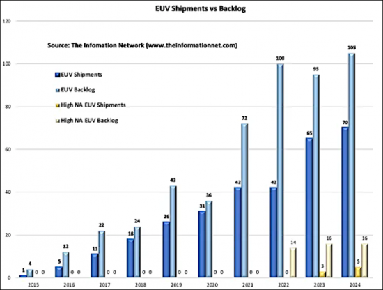
The report provides insights into market share of lithography vendors by equipment type including revenue and unit shipments. Market shares by vendor are provided since 1992. The report identifies and analyzes current and emerging trends driving the semiconductor lithography market, such as node migration, China sanctions, and new semiconductor materials, particularly silicon carbide.
Table of Contents
Chapter 1. Introduction
- 1.1. The Need For This Report
Chapter 2. Executive Summary
- 2.1. Summary of Major Issues
- 2.2. Summary of Market Opportunities
Chapter 3. Lithography Issues And Trends
- 3.1. Optical Systems
- 3.1.1. Introduction
- 3.1.2. Step-and-Repeat Aligners
- 3.1.3. Deep Ultraviolet (DUV)
- 3.2. EUV
- 3.5. Nano-Imprint Lithography
- 3.4. X-Ray Lithography
- 3.3. Electron Beam Lithography
- 3.4. Ion Beam Lithography
Chapter 4. User - Supplier Strategies
- 4.1. Determining Lithography Needs
- 4.2. Benchmarking a Vendor
- 4.2.1. Pricing
- 4.2.2. Vendor Commitment and Attitudes
- 4.2.3. Vendor Capabilities
- 4.2.4. System Capabilities
- 4.2.5. Vendor Feedback During Equipment Evaluation
- 4.2.6. Vendor Feedback During Device Production
- 4.3. Competitive Environment
- 4.4. Equipment For Class 1 Cleanrooms
- 4.5. Equipment For the Factory of the Future
- 4.6. Opportunities
Chapter 5. Market Forecast
- 5.1. Driving Forces
- 5.1.1. Technical Trends
- 5.1.2. Economic Trends
- 5.1.3. Optical Limitations
- 5.2. Market Forecast Assumptions
- 5.3. Market Forecast
List of Tables
- 3.1. Wavelength "Generations"
- 3.2. Characteristics of X-Ray Systems
- 5.1. Worldwide Capital Spending
- 5.2. DRAM Lithographic Requirements
- 5.3. Worldwide Optical Stepper Market
- 5.4. Worldwide Stepper Market Shares
List of Figures
- 1.1. Lithographic Equipment Requirements for DRAMs
- 3.1. Lithography Options For MPUs/DRAMs
- 3.2. Lithography Options For Flash
- 3.3. Illustration of Stepper Exposure System
- 3.4. Lens Arrangement For Submicron Features
- 3.5. Excimer Laser Evolution
- 3.6. EUV Lithography
- 3.7. Thermoplastic Nanoimprint Lithography Process
- 3.8. Step And Flash Nanoimprint Lithography Process
- 3.9. Illustration of X-Ray Lithography
- 3.10. Schematic Of Scalpel Electron Beam System
- 3.11. Multi-Source E-Beam Lithography
- 3.12. Ion Projection Lithography System
- 4.1. Manufacturing Costs Per Exposure Station
- 5.1. Lithography Market Vs Equipment Market
- 5.2. Lithography Double Exposure Technique
- 5.3. Lithography Requirements
- 5.4. Lithography Extensions
- 5.5. Lithography Cost of Ownership
- 5.6. Segmentation of Stepper/Scan Shipments
- 5.7. Market Shares of Vendors (Units)
- 5.8. Unit Market Shares of Vendors
- 5.9. Worldwide I-Line Market Shares
- 5.10. Worldwide 248nm Market Shares
- 5.11. Worldwide 193nm Dry Market Shares
- 5.12. Worldwide 193nm Wet Market Shares
- 5.13. Market Shares of Vendors (Revenues)
 先进半导体材料市场预测至2034年-按材料类型、製造阶段、製造流程、技术节点、应用、最终用户和地区分類的全球分析
 下一代光刻材料市场:按类型、技术、应用和最终用途产业划分-2026-2032年全球市场预测微影术设备市场:2026-2032年全球市场预测(依波长、技术、晶圆尺寸、终端用户产业及应用划分)
 ArFi微影术系统设备市场规模、份额和成长分析:按产品类型、吞吐量、技术、技术节点、应用、最终用户和地区划分 - 2026-2033年产业预测
 微影术设备市场分析及预测(至2035年):依类型、产品、技术、组件、应用、最终用户、製程、安装类型、设备及解决方案划分
 下一代微影术材料市场-全球产业规模、份额、趋势、机会、预测:按材料、应用、地区和竞争对手划分,2021-2031年按软体类型、最终用户、部署类型和製程节点分類的计算微影术软体市场 - 全球预测 2026-2032
 DUV光刻系统市场:按类型、应用、国家和地区划分 - 全球产业分析、市场规模、市场份额及2025-2032年预测
 面向先进节点的下一代微影术技术:技术与应用光刻设备市场规模、占有率、成长及全球产业分析:依类型、应用和地区划分的洞察与预测(2024-2032 年)