


 |
市场调查报告书
商品编码
1721471
雷射光掩模市场机会、成长动力、产业趋势分析及 2025 - 2034 年预测Laser Photomask Market Opportunity, Growth Drivers, Industry Trend Analysis, and Forecast 2025 - 2034 |
||||||
2024 年全球雷射光掩模市场价值为 48 亿美元,预计到 2034 年将以 3% 的复合年增长率成长,达到 64 亿美元。这一增长是由对先进半导体晶片组的需求不断增长、电子元件的持续小型化以及消费性电子产品的激增所推动的。随着半导体技术节点不断缩小至3奈米以下水平,光刻製程的精确度变得更加重要。雷射光掩模对于这种转变至关重要,它能够将复杂的电路图案精确地转移到硅晶片上。这种对精确度的需求正在推动光掩模製造领域的重大创新和投资。
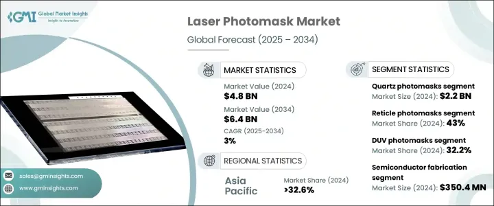
市场正在见证光掩模技术的重大进步,特别是针对日益复杂的半导体应用。随着晶片製造商不断突破製造界限,对高性能光掩模的需求也日益增长,到 2024 年,光罩光掩模市场的价值将达到 20 亿美元。由于该领域在生产尖端光刻技术所需的高解析度图案方面发挥着重要作用,因此其应用范围正在不断扩大。随着极紫外线 (EUV) 和高 NA 光刻技术的兴起,确保无缺陷掩模已成为重中之重,从而导致了能够检测奈米级缺陷的基于 AI 的检测系统的整合。这不仅提高了生产良率,也提高了掩模修復精度。
| 市场范围 | |
|---|---|
| 起始年份 | 2024 |
| 预测年份 | 2025-2034 |
| 起始值 | 48亿美元 |
| 预测值 | 64亿美元 |
| 复合年增长率 | 3% |
石英光掩模市场规模在 2024 年将达到 22 亿美元,仍是市场的主要组成部分,预计到 2034 年复合年增长率将达到 3.2%。该材料卓越的热性能和光学性能使其成为深紫外线 (DUV) 和 EUV 微影製程的理想选择。最近的进展包括使用混合石英坯料结构来最大限度地减少光吸收不一致性,从而显着提高光掩模的品质。这在人工智慧处理器、记忆体模组和其他高精度电子元件的生产中尤其重要,因为光罩的保真度直接影响设备效能。
预计美国雷射光掩模市场到 2024 年将创造 10 亿美元的产值,到 2034 年的复合年增长率将达到 3.6%。这一增长主要得益于本地化半导体製造需求的不断增长,以及政策激励和技术进步的支持。对人工智慧运算的需求不断增长,增加了对先进半导体节点的需求,进一步推动了光掩模的消费。随着美国境内更多半导体工厂的建设,对最先进光掩模的需求预计将持续上升。
应用材料公司(Applied Materials Inc.)、Photronics Inc.、KLA Corporation 等领先公司处于市场前沿。为了保持竞争优势,这些公司正在采用先进的自动化和人工智慧技术来简化检查流程、提高产量并最大限度地减少缺陷。他们还专注于开发与 EUV 相容的光掩模,并与半导体代工厂合作,为 3nm 以下节点量身定制掩模。扩大半导体中心的生产设施和增加下一代掩模材料的研发支出是满足不断增长的产业需求和确保市场领导地位的核心策略。
目录
第一章:方法论与范围
第二章:执行摘要
第三章:行业洞察
- 产业生态系统分析
- 供应商矩阵
- 利润率分析
- 技术与创新格局
- 专利分析
- 重要新闻和倡议
- 产业衝击力
- 成长动力
- 半导体晶片组需求不断成长
- 电子元件快速小型化
- 消费性电子产品市场的扩张
- 提升品牌形象与市场差异化
- 增加半导体研发投入
- 产业陷阱与挑战
- 高资本支出和生产成本
- 硅供应链的脆弱性
- 成长动力
- 成长潜力分析
- 波特的分析
- PESTEL分析
- 未来市场趋势
- 监管格局
第四章:市场估计与预测:按光掩模类型,2021 年至 2034 年
- 主要趋势
- 光罩
- 主光掩模
- 复製光掩模
第五章:市场估计与预测:依基板材料,2021 年至 2034 年
- 主要趋势
- 石英光掩模
- 钠钙光掩模
- 薄膜光掩模
第六章:市场估计与预测:按技术,2021 年至 2034 年
- 主要趋势
- EUV(极紫外线)光掩模
- DUV(深紫外线)光掩模
- 二元光掩模
- 相移光掩模
第七章:市场估计与预测:按应用,2021 年至 2034 年
- 主要趋势
- 半导体製造
- 平面显示器製造
- MEMS(微机电系统)
- IC封装
- 光电子
- 其他
第八章:市场估计与预测:按最终用途产业,2021 年至 2034 年
- 主要趋势
- 消费性电子产品
- 汽车
- 医疗保健和医疗器械
- 航太与国防
- 电信
- 其他的
第九章:市场估计与预测:按地区,2021–2034
- 主要趋势
- 北美洲
- 我们
- 加拿大
- 欧洲
- 德国
- 英国
- 法国
- 西班牙
- 义大利
- 欧洲其他地区
- 亚太地区
- 日本
- 中国
- 印度
- 韩国
- 澳新银行
- 亚太其他地区
- 拉丁美洲
- 巴西
- 墨西哥
- 拉丁美洲其他地区
- 中东和非洲
- 南非
- 阿联酋
- 沙乌地阿拉伯
- 中东和非洲其他地区
第十章:公司简介
- Applied Materials Inc.
- KLA Corporation
- Photronics Inc.
- Toppan Photomasks, Inc.
- Dai Nippon Printing Co., Ltd. (DNP)
- Hoya Corporation
- LG Innotek Co., Ltd.
- SK-Electronics Co., Ltd.
- Compugraphics
- Nippon Filcon Co., Ltd.
- Lasertec Corporation
- Taiwan Mask Corporation (TMC)
- Qingyi Photomask Limited
- Hua Hong Semiconductor
- SUSS MicroTec SE
- Mycronic AB
- Carl Zeiss SMT GmbH
- Canon Inc.
- ASML Holding NV
- Nikon Corporation
- JEOL Ltd.
- Veeco Instruments Inc.
The Global Laser Photomask Market was valued at USD 4.8 billion in 2024 and is estimated to grow at a CAGR of 3% to reach USD 6.4 billion by 2034. This growth is being driven by the increasing demand for advanced semiconductor chipsets, the ongoing miniaturization of electronic components, and a surge in consumer electronics. As semiconductor technology nodes continue shrinking to sub-3nm levels, precision in lithographic processes has become more critical. Laser photomasks are crucial to this transformation, enabling the accurate transfer of complex circuit patterns onto silicon wafers. This need for precision is fueling significant innovation and investment in the photomask manufacturing sector.
The market is witnessing significant advancements in photomask technology, particularly in response to the growing complexity of semiconductor applications. As chipmakers push the boundaries of fabrication, there is an increasing demand for high-performance photomasks, with the reticle photomask segment valued at USD 2 billion in 2024. This segment is seeing greater adoption due to its essential role in producing the high-resolution patterns needed for cutting-edge lithography. With the rise of extreme ultraviolet (EUV) and high-NA lithography, ensuring defect-free masks has become a top priority, leading to the integration of AI-based inspection systems that can detect defects at the nanometer scale. This not only enhances production yield but also improves mask repair accuracy.
| Market Scope | |
|---|---|
| Start Year | 2024 |
| Forecast Year | 2025-2034 |
| Start Value | $4.8 Billion |
| Forecast Value | $6.4 Billion |
| CAGR | 3% |
Quartz photomasks, accounting for USD 2.2 billion in 2024, remain a dominant segment in the market, projected to grow at a CAGR of 3.2% through 2034. The material's exceptional thermal and optical properties make it ideal for deep ultraviolet (DUV) and EUV lithography processes. Recent advancements include the use of hybrid quartz-blank structures to minimize light absorption inconsistencies, significantly improving the quality of photomasks. This is especially important in the production of AI processors, memory modules, and other high-precision electronic components, where the fidelity of the mask directly affects device performance.
The United States Laser Photomask Market is estimated to generate USD 1 billion in 2024, growing at a CAGR of 3.6% through 2034. This growth is fueled by the rising demand for localized semiconductor manufacturing, supported by policy incentives and technological advances. The accelerating need for AI-powered computing has increased demand for advanced semiconductor nodes, further driving photomask consumption. With the construction of more semiconductor fabs within the U.S., the demand for state-of-the-art photomasks is expected to continue rising.
Leading companies such as Applied Materials Inc., Photronics Inc., and KLA Corporation are at the forefront of the market. To maintain a competitive edge, these companies are adopting advanced automation and AI technologies to streamline inspection processes, improve yield, and minimize defects. They are also focusing on developing EUV-compatible photomasks and collaborating with semiconductor foundries to create masks tailored for sub-3nm nodes. Expanding production facilities in semiconductor hubs and increasing R&D spending on next-gen mask materials are central strategies to meet growing industry demands and secure market leadership.
Table of Contents
Chapter 1 Methodology & Scope
- 1.1 Market scope & definitions
- 1.2 Research design
- 1.2.1 Research approach
- 1.2.2 Data collection methods
- 1.3 Base estimates & calculations
- 1.3.1 Base year calculation
- 1.3.2 Key trends for market estimation
- 1.4 Forecast model
- 1.5 Primary research and validation
- 1.5.1 Primary sources
- 1.5.2 Data mining sources
Chapter 2 Executive Summary
- 2.1 Industry 3600 synopsis
Chapter 3 Industry Insights
- 3.1 Industry ecosystem analysis
- 3.2 Vendor matrix
- 3.3 Profit margin analysis
- 3.4 Technology & innovation landscape
- 3.5 Patent analysis
- 3.6 Key news and initiatives
- 3.7 Industry impact forces
- 3.7.1 Growth drivers
- 3.7.1.1 Growing demand for semiconductor chipsets
- 3.7.1.2 Rapid miniaturization of electronic components
- 3.7.1.3 Expansion of the consumer electronics market
- 3.7.1.4 Enhanced Brand Image and Market Differentiation
- 3.7.1.5 Increased investment in semiconductor R&D
- 3.7.2 Industry pitfalls & challenges
- 3.7.2.1 High capital expenditure and production costs
- 3.7.2.2 Vulnerability to the silicon supply chain
- 3.7.1 Growth drivers
- 3.8 Growth potential analysis
- 3.9 Porter’s analysis
- 3.10 PESTEL analysis
- 3.11 Future market trends
- 3.12 Regulatory landscape
Chapter 4 Market Estimates and Forecast, By Photomask Type, 2021 – 2034 (USD Million & Million Units)
- 4.1 Key trends
- 4.2 Reticle photomasks
- 4.3 Master photomasks
- 4.4 Replicated photomasks
Chapter 5 Market Estimates and Forecast, By Substrate Material, 2021 – 2034 (USD Million & Million Units)
- 5.1 Key trends
- 5.2 Quartz photomasks
- 5.3 Soda-lime photomasks
- 5.4 Film photomasks
Chapter 6 Market Estimates and Forecast, By Technology, 2021 – 2034 (USD Million & Million Units)
- 6.1 Key trends
- 6.2 EUV (Extreme Ultraviolet) photomasks
- 6.3 DUV (Deep Ultraviolet) photomasks
- 6.4 Binary photomasks
- 6.5 Phase shift photomasks
Chapter 7 Market Estimates and Forecast, By Application, 2021 – 2034 (USD Million & Million Units)
- 7.1 Key trends
- 7.2 Semiconductor fabrication
- 7.3 Flat panel display manufacturing
- 7.4 MEMS (Micro-Electromechanical Systems)
- 7.5 IC packaging
- 7.6 Optoelectronics
- 7.7 Other
Chapter 8 Market Estimates and Forecast, By End Use Industry, 2021 – 2034 (USD Million & Million Units)
- 8.1 Key trends
- 8.2 Consumer electronics
- 8.3 Automotive
- 8.4 Healthcare & medical devices
- 8.5 Aerospace & defense
- 8.6 Telecommunication
- 8.7 Others
Chapter 9 Market Estimates and Forecast, By Region, 2021– 2034 (USD Million & Million Units)
- 9.1 Key trends
- 9.2 North America
- 9.2.1 U.S.
- 9.2.2 Canada
- 9.3 Europe
- 9.3.1 Germany
- 9.3.2 UK
- 9.3.3 France
- 9.3.4 Spain
- 9.3.5 Italy
- 9.3.6 Rest of Europe
- 9.4 Asia Pacific
- 9.4.1 Japan
- 9.4.2 China
- 9.4.3 India
- 9.4.4 South Korea
- 9.4.5 ANZ
- 9.4.6 Rest of Asia Pacific
- 9.5 Latin America
- 9.5.1 Brazil
- 9.5.2 Mexico
- 9.5.3 Rest of Latin America
- 9.6 Middle East and Africa
- 9.6.1 South Africa
- 9.6.2 UAE
- 9.6.3 Saudi Arabia
- 9.6.4 Rest of Middle East and Africa
Chapter 10 Company Profiles
- 10.1 Applied Materials Inc.
- 10.2 KLA Corporation
- 10.3 Photronics Inc.
- 10.4 Toppan Photomasks, Inc.
- 10.5 Dai Nippon Printing Co., Ltd. (DNP)
- 10.6 Hoya Corporation
- 10.7 LG Innotek Co., Ltd.
- 10.8 SK-Electronics Co., Ltd.
- 10.9 Compugraphics
- 10.10 Nippon Filcon Co., Ltd.
- 10.11 Lasertec Corporation
- 10.12 Taiwan Mask Corporation (TMC)
- 10.13 Qingyi Photomask Limited
- 10.14 Hua Hong Semiconductor
- 10.15 SUSS MicroTec SE
- 10.16 Mycronic AB
- 10.17 Carl Zeiss SMT GmbH
- 10.18 Canon Inc.
- 10.19 ASML Holding N.V.
- 10.20 Nikon Corporation
- 10.21 JEOL Ltd.
- 10.22 Veeco Instruments Inc.
 半导体掩模服务市场:依最终用户、应用、製程节点、服务、掩模类型和晶圆尺寸划分,全球预测,2026-2032年
 2026年全球雷射光掩模市场报告全球晶片光掩模市场报告(2026 年)光掩模清洗系统市场按产品类型、清洗技术、掩模类型和最终用户划分 - 全球预测 2026-2032半导体掩模坯市场:产品类型、材料类型、微影术节点、晶圆尺寸、涂层类型、应用和最终用户 - 全球预测,2026-2032年
 雷射光掩模市场-2025-2030年预测
 半导体掩模检测设备:全球市占率及排名、总收入及需求预测(2025-2031年)光掩模和掩模坯:全球市场份额和排名、总收入和需求预测(2025-2031年)掩模坯料:全球市场份额和排名、总收入和需求预测(2025-2031年)
 光掩模市场规模、份额、趋势及预测(按产品、掩模车间类型、应用和地区划分)2025 年至 2033 年