


 |
市场调查报告书
商品编码
1892717
原子层蚀刻(ALE)设备市场机会、成长驱动因素、产业趋势分析及预测(2025-2034年)Atomic Layer Etching (ALE) Equipment Market Opportunity, Growth Drivers, Industry Trend Analysis, and Forecast 2025 - 2034 |
||||||
2024 年全球原子层蚀刻设备市场价值为 11 亿美元,预计到 2034 年将以 8.5% 的复合年增长率增长至 25 亿美元。
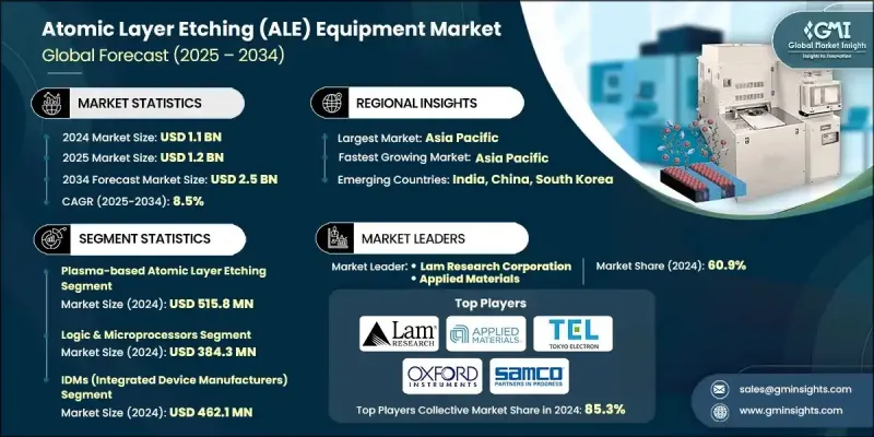
推动成长的因素包括:对紧凑型、高性能半导体元件日益增长的需求、量子技术的快速发展以及对节能电子产品的需求。此外,各公司也积极回应新材料的应用以及装置小型化趋势,而这需要具备原子级精度的蚀刻能力。随着下一代晶片的复杂性不断提升,业界正大力转向能够支援复杂架构的先进工具。量子研究带来的发展动能也进一步推动了对高精度蚀刻技术的需求,这些技术有助于改进极度敏感元件的製造。
| 市场范围 | |
|---|---|
| 起始年份 | 2024 |
| 预测年份 | 2025-2034 |
| 起始值 | 11亿美元 |
| 预测值 | 25亿美元 |
| 复合年增长率 | 8.5% |
2024 年,基于等离子体的原子层蚀刻市场规模达到 5.158 亿美元。微电子产业的持续扩张促使供应商增强等离子体原子层蚀刻产品组合,以提供更高的精度、更好的蚀刻选择性和更严格的材料控制,从而满足先进製造环境中不断增长的生产需求。
2025年至2034年间,先进封装元件市场将以11.4%的复合年增长率成长。其成长主要得益于不断提升的性能需求、5G连接的普及以及在不重新设计核心装置的情况下整合更多功能的需求。为了满足现代电子系统不断变化的封装需求,各公司正优先推动热效率、小型化和高密度互连技术的创新。
2024年,美国原子层蚀刻设备市场规模预计将达2.002亿美元。这一成长主要得益于联邦政府对半导体产能的资助、人工智慧和物联网的蓬勃发展、先进製造流程的进步以及国防应用领域需求的激增。在该地区营运的企业正积极利用投资激励措施,强化下一代工艺能力,并满足航太和国防客户的复杂需求。
目录
第一章:方法论与范围
第二章:执行概要
第三章:行业洞察
- 产业生态系分析
- 供应商格局
- 利润率
- 成本结构
- 每个阶段的价值增加
- 影响价值链的因素
- 中断
- 产业生态系分析
- 产业影响因素
- 成长驱动因素
- 对更小、更强大的半导体装置的需求日益增长
- 量子计算的进展
- 对高性能和节能电子产品的需求日益增长
- 先进电子元件新材料的涌现
- 对小型化和复杂积体电路的需求不断增长
- 陷阱与挑战
- ALE设备成本高昂
- 与现有製造流程整合的复杂性
- 市场机会
- 对先进半导体技术的需求不断增长
- 物联网和人工智慧新兴应用的成长
- 成长驱动因素
- 成长潜力分析
- 监管环境
- 北美洲
- 欧洲
- 亚太地区
- 拉丁美洲
- 中东和非洲
- 波特的分析
- PESTEL 分析
- 技术与创新格局
- 当前技术趋势
- 新兴技术
- 价格趋势
- 按地区
- 副产品
- 定价策略
- 新兴商业模式
- 合规要求
- 永续性措施
- 消费者情绪分析
- 专利和智慧财产权分析
- 地缘政治与贸易动态
第四章:竞争格局
- 介绍
- 公司市占率分析
- 按地区
- 北美洲
- 欧洲
- 亚太地区
- 拉丁美洲
- 中东和非洲
- 市场集中度分析
- 按地区
- 对主要参与者进行竞争基准分析
- 财务绩效比较
- 收入
- 利润率
- 研发
- 产品组合比较
- 产品范围广度
- 科技
- 创新
- 地理位置比较
- 全球足迹分析
- 服务网路覆盖
- 按地区分類的市场渗透率
- 竞争定位矩阵
- 领导人
- 挑战者
- 追踪者
- 小众玩家
- 战略展望矩阵
- 财务绩效比较
- 2021-2024 年主要发展动态
- 併购
- 伙伴关係与合作
- 技术进步
- 扩张和投资策略
- 永续发展倡议
- 数位转型计划
- 新兴/新创企业竞争对手格局
第五章:市场估计与预测:依技术划分,2021-2034年
- 基于等离子体的原子层蚀刻
- 离子束原子层蚀刻
- 热原子层蚀刻
- 混合原子层蚀刻
- 其他的
第六章:市场估算与预测:依应用领域划分,2021-2034年
- 逻辑与微处理器
- 储存装置
- 功率和射频元件
- 先进包装
- 光电子学与光子学
- MEMS和感测器
- 其他的
第七章:市场估算与预测:依晶圆尺寸划分,2021-2034年
- 200毫米
- 300毫米
- 450毫米
第八章:市场估算与预测:依最终用途划分,2021-2034年
- IDM(整合设备製造商)
- 铸造厂
- 记忆体製造商
- OSAT/包装厂
- 其他的
第九章:市场估计与预测:依地区划分,2021-2034年
- 北美洲
- 我们
- 加拿大
- 欧洲
- 德国
- 英国
- 法国
- 西班牙
- 义大利
- 荷兰
- 亚太地区
- 中国
- 印度
- 日本
- 澳洲
- 韩国
- 拉丁美洲
- 巴西
- 墨西哥
- 阿根廷
- 中东和非洲
- 沙乌地阿拉伯
- 南非
- 阿联酋
第十章:公司简介
- 全球关键参与者
- Lam Research Corporation
- Applied Materials
- Tokyo Electron
- Hitachi High Tech Corporation
- 区域关键参与者
- 北美洲
- Mattson Technology, Inc.
- Plasma-Therm
- 欧洲
- Oxford Instruments
- Asia-Pacific
- Samco Inc.
- Nano Vacuum Pty Ltd
- 北美洲
- 颠覆者/小众玩家
- CORIAL
The Global Atomic Layer Etching Equipment Market was valued at USD 1.1 billion in 2024 and is estimated to grow at a CAGR of 8.5% to reach USD 2.5 billion by 2034.
Growth is fueled by rising demand for compact, high-performance semiconductor components, rapid advancements in quantum technologies, and the push for energy-efficient electronics. Companies are also responding to the adoption of new materials and the ongoing trend toward greater device miniaturization, which requires etching capabilities with atomic-level precision. As next-generation chips continue to increase in complexity, the industry is seeing a strong shift toward advanced tools capable of supporting sophisticated architecture. The momentum generated by quantum research is also boosting the need for highly accurate etching techniques that improve the fabrication of extremely sensitive components.
| Market Scope | |
|---|---|
| Start Year | 2024 |
| Forecast Year | 2025-2034 |
| Start Value | $1.1 billion |
| Forecast Value | $2.5 billion |
| CAGR | 8.5% |
The plasma-based atomic layer etching segment held USD 515.8 million in 2024. Continued expansion in microelectronics is encouraging suppliers to enhance plasma ALE portfolios that deliver greater precision, improved etch selectivity, and tighter material control to meet rising production requirements across advanced manufacturing environments.
The advanced packaging devices segment will grow at 11.4% CAGR between 2025 and 2034. Its growth is linked to increasing performance demands, the spread of 5G connectivity, and the need to integrate more functionality without redesigning core devices. Companies are prioritizing innovations in thermal efficiency, miniaturization, and high-density interconnect technologies to support evolving packaging requirements in modern electronic systems.
United States Atomic Layer Etching Equipment Market generated USD 200.2 million in 2024. This expansion stems from federal funding for semiconductor capacity, a surge in AI and IoT development, progress in advanced manufacturing nodes, and elevated demand from defense-oriented applications. Companies operating in the region are leveraging investment incentives, strengthening next-generation process capabilities, and addressing the sophisticated needs of aerospace and defense customers.
Key players in the Atomic Layer Etching Equipment Market include Lam Research Corporation, CORIAL, NAURA, Mattson Technology, Inc., Oxford Instruments, Samco Inc., Tokyo Electron, Applied Materials, Hitachi High-Tech Corporation, and Nano Vacuum Pty Ltd. Companies competing in the Atomic Layer Etching Equipment Market are adopting strategic measures to reinforce their global positions. Many are investing heavily in R&D programs to enhance precision, boost throughput, and improve compatibility with emerging materials. Businesses are also expanding collaboration with semiconductor manufacturers to co-develop etch solutions aligned with next-generation device architectures. Several players are strengthening production capacity and broadening product portfolios to address varied fabrication needs. Firms are increasing their presence in high-growth regions by forming local partnerships and establishing technical support centers.
Table of Contents
Chapter 1 Methodology and scope
- 1.1 Market scope and definition
- 1.2 Research design
- 1.2.1 Research approach
- 1.2.2 Data collection methods
- 1.3 Data mining sources
- 1.3.1 Global
- 1.3.2 Regional/Country
- 1.4 Base estimates and calculations
- 1.4.1 Base year calculation
- 1.4.2 Key trends for market estimation
- 1.5 Primary research and validation
- 1.5.1 Primary sources
- 1.6 Forecast model
- 1.7 Research assumptions and limitations
Chapter 2 Executive summary
- 2.1 Industry 3600 synopsis
- 2.2 Key market trends
- 2.2.1 Technology trend
- 2.2.2 Application trends
- 2.2.3 Wafer size trends
- 2.2.4 End use industry trends
- 2.2.5 Regional trends
- 2.3 TAM Analysis, 2025-2034 (USD Million)
- 2.4 CXO perspectives: Strategic imperatives
- 2.4.1 Executive decision points
- 2.4.2 critical success factors
- 2.5 Future outlook and strategic recommendations
Chapter 3 Industry insights
- 3.1 Industry ecosystem analysis
- 3.1.1 Supplier landscape
- 3.1.2 Profit margin
- 3.1.3 Cost structure
- 3.1.4 Value addition at each stage
- 3.1.5 Factor affecting the value chain
- 3.1.6 Disruptions
- 3.2 Industry ecosystem analysis
- 3.3 Industry impact forces
- 3.3.1 Growth drivers
- 3.3.1.1 Increasing Demand for Smaller and More Powerful Semiconductor Devices
- 3.3.1.2 Advancements in Quantum Computing
- 3.3.1.3 Growing Demand for High-Performance and Energy-Efficient Electronics
- 3.3.1.4 Emergence of New Materials for Advanced Electronics
- 3.3.1.5 Rising Demand for Miniaturized and Complex Integrated Circuits
- 3.3.2 Pitfalls and challenges
- 3.3.2.1 High Cost of ALE Equipment
- 3.3.2.2 Complexity in Integration with Existing Manufacturing Processes
- 3.3.3 Market opportunities
- 3.3.3.1 Rising Demand for Advanced Semiconductor Technologies
- 3.3.3.2 Growth of Emerging Applications in IoT and AI
- 3.3.1 Growth drivers
- 3.4 Growth potential analysis
- 3.5 Regulatory landscape
- 3.5.1 North America
- 3.5.2 Europe
- 3.5.3 Asia Pacific
- 3.5.4 Latin America
- 3.5.5 Middle East & Africa
- 3.6 Porter's analysis
- 3.7 PESTEL analysis
- 3.8 Technology and Innovation landscape
- 3.8.1 Current technological trends
- 3.8.2 Emerging technologies
- 3.9 Price trends
- 3.9.1 By region
- 3.9.2 By product
- 3.10 Pricing Strategies
- 3.11 Emerging Business Models
- 3.12 Compliance Requirements
- 3.13 Sustainability Measures
- 3.14 Consumer Sentiment Analysis
- 3.15 Patent and IP analysis
- 3.16 Geopolitical and trade dynamics
Chapter 4 Competitive landscape, 2024
- 4.1 Introduction
- 4.2 Company market share analysis
- 4.2.1 By region
- 4.2.1.1 North America
- 4.2.1.2 Europe
- 4.2.1.3 Asia Pacific
- 4.2.1.4 Latin America
- 4.2.1.5 Middle East & Africa
- 4.2.2 Market concentration analysis
- 4.2.1 By region
- 4.3 Competitive benchmarking of key players
- 4.3.1 Financial performance comparison
- 4.3.1.1 Revenue
- 4.3.1.2 Profit margin
- 4.3.1.3 R&D
- 4.3.2 Product portfolio comparison
- 4.3.2.1 Product range breadth
- 4.3.2.2 Technology
- 4.3.2.3 Innovation
- 4.3.3 Geographic presence comparison
- 4.3.3.1 Global footprint analysis
- 4.3.3.2 Service network coverage
- 4.3.3.3 Market penetration by region
- 4.3.4 Competitive positioning matrix
- 4.3.4.1 Leaders
- 4.3.4.2 Challengers
- 4.3.4.3 Followers
- 4.3.4.4 Niche players
- 4.3.5 Strategic outlook matrix
- 4.3.1 Financial performance comparison
- 4.4 Key developments, 2021-2024
- 4.4.1 Mergers and acquisitions
- 4.4.2 Partnerships and collaborations
- 4.4.3 Technological advancements
- 4.4.4 Expansion and investment strategies
- 4.4.5 Sustainability initiatives
- 4.4.6 Digital transformation initiatives
- 4.5 Emerging/ startup competitors landscape
Chapter 5 Market estimates and forecast, by Technology, 2021 - 2034 (USD Million & Units)
- 5.1 Key trends
- 5.2 Plasma-based atomic layer etching
- 5.3 Ion beam atomic layer etching
- 5.4 Thermal atomic layer etching
- 5.5 Hybrid atomic layer etching
- 5.6 Others
Chapter 6 Market estimates and forecast, By Application, 2021 - 2034 (USD Million & Units)
- 6.1 Key trends
- 6.2 Logic & microprocessors
- 6.3 Memory devices
- 6.4 Power & RF devices
- 6.5 Advanced packaging
- 6.6 Optoelectronics & photonics
- 6.7 MEMS & sensors
- 6.8 Others
Chapter 7 Market estimates and forecast, By Wafer Size, 2021 - 2034 (USD Million & Units)
- 7.1 Key trends
- 7.2 200 mm
- 7.3 300 mm
- 7.4 450 mm
Chapter 8 Market estimates and forecast, By End Use, 2021 - 2034 (USD Million & Units)
- 8.1 Key trends
- 8.2 IDMs (integrated device manufacturers)
- 8.3 Foundries
- 8.4 Memory manufacturers
- 8.5 OSATs / packaging houses
- 8.6 Others
Chapter 9 Market estimates and forecast, By Region, 2021 - 2034 (USD Million & Units)
- 9.1 Key trends
- 9.2 North America
- 9.2.1 U.S.
- 9.2.2 Canada
- 9.3 Europe
- 9.3.1 Germany
- 9.3.2 UK
- 9.3.3 France
- 9.3.4 Spain
- 9.3.5 Italy
- 9.3.6 Netherlands
- 9.4 Asia Pacific
- 9.4.1 China
- 9.4.2 India
- 9.4.3 Japan
- 9.4.4 Australia
- 9.4.5 South Korea
- 9.5 Latin America
- 9.5.1 Brazil
- 9.5.2 Mexico
- 9.5.3 Argentina
- 9.6 Middle East and Africa
- 9.6.1 Saudi Arabia
- 9.6.2 South Africa
- 9.6.3 UAE
Chapter 10 Company profiles
- 10.1 Global Key Players
- 10.1.1 Lam Research Corporation
- 10.1.2 Applied Materials
- 10.1.3 Tokyo Electron
- 10.1.4 Hitachi High Tech Corporation
- 10.2 Regional Key Players
- 10.2.1 North America
- 10.2.1.1 Mattson Technology, Inc.
- 10.2.1.2 Plasma-Therm
- 10.2.2 Europe
- 10.2.2.1 Oxford Instruments
- 10.2.3 Asia-Pacific
- 10.2.3.1 Samco Inc.
- 10.2.3.2 Nano Vacuum Pty Ltd
- 10.2.1 North America
- 10.3 Disruptors / Niche Players
- 10.3.1 CORIAL
 全球高阶ALD设备市场(按设备类型、技术类型、晶圆尺寸、应用和最终用户产业划分)预测(2026-2032年)
 全球原子层沉积元件市场规模、份额、趋势和成长分析报告(2026-2034年)原子层沉积(ALD)全球市场规模、份额、趋势和成长分析报告,2026-2034年
 2026年全球原子层沉积市场报告2026年全球ALD设备市场报告
 2026-2030年全球原子层沉积(ALD)市场半导体以六氯二硅烷市场:依沉积技术、晶圆直径、纯度等分類的全球预测,2026-2032年原子层沉积设备市场-2025-2030年预测
 原子层沉积(ALD)前驱体市场机会、成长驱动因素、产业趋势分析及预测(2025-2034年)
 原子层沉积(ALD)设备-全球市场份额和排名、总收入和需求预测(2025-2031年)