


 |
市场调查报告书
商品编码
1928874
薄晶圆加工切割设备市场机会、成长要素、产业趋势分析及2026年至2035年预测Thin Wafer Processing and Dicing Equipment Market Opportunity, Growth Drivers, Industry Trend Analysis, and Forecast 2026 - 2035 |
||||||
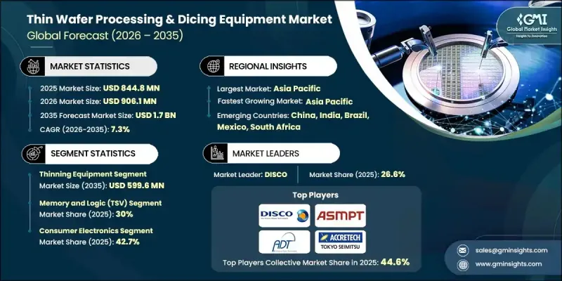
全球薄晶圆加工和切割设备市场预计到 2025 年将达到 8.448 亿美元,到 2035 年将达到 17 亿美元,年复合成长率为 7.3%。
半导体装置日益复杂化以及后端製造对更高精度的需求推动了市场成长。对更薄、更轻、更可靠的组件的需求不断增长,并持续改变整个价值链的设备要求。装置结构和材料的进步使得精度、产量比率和材料应力的降低成为关注的焦点。设备供应商正积极回应,提供先进的解决方案,以实现晶圆的精确减薄和分离,同时保持结构完整性。新一代封装技术的应用进一步提升了对高精度製程的需求。製造商优先考虑生产效率、成本效益和製程稳定性,以支援大规模半导体生产。自动化和智慧系统在提高产能、减少停机时间和加强品管发挥越来越重要的作用。这些因素共同作用,使得薄晶圆加工和切割设备成为全球半导体产业创新和规模化发展的关键驱动力。
| 市场覆盖范围 | |
|---|---|
| 开始年份 | 2025 |
| 预测年份 | 2026-2035 |
| 起始值 | 8.448亿美元 |
| 预测金额 | 17亿美元 |
| 复合年增长率 | 7.3% |
设备供应商不断改进非接触式、低应力加工技术,以提高产量比率并支援日益脆弱的晶圆结构。对尺寸精度、表面品质和运作效率的日益重视,反映了整个产业朝向更高元件密度迈进的趋势。自动化和数据驱动系统有助于改善整个生产线的製程控制、减少缺陷并进行预测性维护。
预计到2035年,薄膜设备市场规模将达到5.996亿美元。随着半导体製造商向支援紧凑型高性能元件的超薄晶圆转型,市场需求不断增长。精密加工技术的持续改进有助于提高产量比率、降低应力水平,并增强与先进元件製造中使用的精密晶圆的兼容性。
预计2026年至2035年间,MEMS装置市场将以8.6%的复合年增长率成长。成长的主要驱动力是众多终端应用产业对紧凑、可靠、高精度元件的需求不断增长。超薄晶圆处理和先进分离技术的日益普及提高了装置的一致性和可靠性。自动化和即时监控系统则进一步促进了产量比率的最佳化。
欧洲薄晶圆加工和切割设备市场预计到2025年将达到1.614亿美元,并在整个预测期内保持强劲成长。区域需求得益于对先进半导体製造的持续投资,尤其是在多个行业的高性能和高精度应用领域。
目录
第一章调查方法和范围
第二章执行摘要
第三章业界考察
- 生态系分析
- 供应商情况
- 利润率分析
- 成本结构
- 每个阶段的附加价值
- 影响价值链的因素
- 中断
- 产业影响因素
- 司机
- 对小型化电子设备的需求不断增长
- 5G和高效能运算应用的普及
- 扩大先进半导体材料的应用
- 汽车电子和电动车(EV)的成长
- 产业潜在风险与挑战
- 先进切割设备高成本
- 薄晶圆的脆弱性日益增加
- 市场机会
- 将晶圆处理与人工智慧和自动化技术结合
- MEMS、光学和射频元件製造领域的成长
- 司机
- 成长潜力分析
- 监管环境
- 北美洲
- 欧洲
- 亚太地区
- 拉丁美洲
- 中东和非洲
- 波特分析
- PESTEL 分析
- 科技与创新趋势
- 当前技术趋势
- 新兴技术
- 新兴经营模式
- 合规要求
- 专利和智慧财产权分析
- 地缘政治和贸易趋势
第四章 竞争情势
- 介绍
- 公司市占率分析
- 按地区
- 北美洲
- 欧洲
- 亚太地区
- 拉丁美洲
- 中东和非洲
- 按地区
- 主要企业的竞争标竿分析
- 财务绩效比较
- 收入
- 利润率
- 研究与开发
- 产品系列比较
- 产品线的广度
- 科技
- 创新
- 区域比较
- 全球扩张分析
- 服务网路覆盖
- 按地区分類的市场渗透率
- 竞争定位矩阵
- 领导企业
- 受让人
- 追踪者
- 小众玩家
- 战略展望矩阵
- 财务绩效比较
- 2021-2024 年主要发展动态
- 併购
- 合作伙伴关係和合资企业
- 技术进步
- 扩张与投资策略
- 数位转型计划
- 新兴/Start-Ups竞赛的趋势
第五章 依设备类型分類的市场估算与预测,2022-2035年
- 薄膜设备
- 切丁设备
- 刀切
- 雷射切割
- 隐密骰子
- 等离子切割
- 搬运辅助设备
- 临时黏合/脱黏系统
- 晶圆安装/拆卸系统
- 清洁和检查系统
第六章 依晶圆尺寸分類的市场估算与预测,2022-2035年
- 小于4英寸
- 5英寸和6英寸
- 8吋
- 12英吋
第七章 依晶圆厚度分類的市场估计与预测,2022-2035年
- 750µm(标准/相对较厚)
- 120µm(先进主流)
- 50微米或更小
第八章 按应用领域分類的市场估算与预测,2022-2035年
- CMOS影像感测器
- 记忆体和逻辑(TSV)
- MEMS元件
- 功率元件
- RFID
- 其他的
9. 2022-2035年按最终用途产业分類的市场估算与预测
- 家用电子电器
- 车
- 电讯
- 卫生保健
- 航太/国防
- 工业的
- 其他的
第十章 2022-2035年各地区市场估计与预测
- 北美洲
- 我们
- 加拿大
- 欧洲
- 德国
- 英国
- 法国
- 西班牙
- 义大利
- 荷兰
- 亚太地区
- 中国
- 印度
- 日本
- 澳洲
- 韩国
- 拉丁美洲
- 巴西
- 墨西哥
- 阿根廷
- 中东和非洲
- 南非
- 沙乌地阿拉伯
- 阿拉伯聯合大公国
第十一章 公司简介
- 主要企业
- DISCO Corporation
- ASMPT
- KLA Corporation
- Lam Research Corporation
- 按地区分類的主要企业
- 北美洲
- Plasma-Therm
- SPTS Technologies Ltd.
- Loadpoint Ltd.
- 欧洲
- Synova SA
- Modutek Corporation
- Dynatex International
- 亚太地区
- Tokyo Electron Limited
- TOKYO SEIMITSU CO., LTD(Accretech)
- Panasonic Connect Co., Ltd.
- 北美洲
- 小众玩家/颠覆者
- Advanced Dicing Technologies
- AXUS TECHNOLOGY
- Citizen Chiba Precision Co., Ltd.
- HANMI Semiconductor
- Han's Laser Technology Co., Ltd.
- NeonTech Co.,Ltd.
- Suzhou Delphi Laser Co., Ltd.
The Global Thin Wafer Processing & Dicing Equipment Market was valued at USD 844.8 million in 2025 and is estimated to grow at a CAGR of 7.3% to reach USD 1.7 billion by 2035.
Market growth is supported by the rising complexity of semiconductor devices and the need for higher precision during backend manufacturing. Increasing demand for thinner, lighter, and more reliable components continues to reshape equipment requirements across the value chain. Advancements in device architecture and materials place greater emphasis on accuracy, yield improvement, and reduced material stress. Equipment suppliers respond by delivering advanced solutions that enable precise wafer thinning and separation while maintaining structural integrity. The adoption of next-generation packaging approaches further intensifies demand for high-precision processes. Manufacturers prioritize productivity, cost efficiency, and process stability to support large-scale semiconductor production. Automation and intelligent systems play an expanding role in improving throughput, reducing downtime, and enhancing quality control. Together, these factors establish thin wafer processing and dicing equipment as a critical enabler of innovation and scalability within the global semiconductor industry.
| Market Scope | |
|---|---|
| Start Year | 2025 |
| Forecast Year | 2026-2035 |
| Start Value | $844.8 Million |
| Forecast Value | $1.7 Billion |
| CAGR | 7.3% |
Equipment suppliers continue to advance non-contact and low-stress processing technologies to improve yields and support increasingly fragile wafer structures. Greater focus on dimensional accuracy, surface quality, and operational efficiency reflects broader industry trends toward higher device density. Automation and data-driven systems support improved process control, defect reduction, and predictive maintenance across manufacturing lines.
The thinning equipment segment is expected to reach USD 599.6 million by 2035. Demand rises as semiconductor producers move toward ultra-thin wafers to support compact and high-performance devices. Ongoing improvements in precision processing techniques contribute to better yield rates, lower stress levels, and enhanced compatibility with delicate wafers used in advanced device fabrication.
The MEMS devices segment is forecast to grow at a CAGR of 8.6% between 2026 and 2035. Growth is driven by expanding adoption across multiple end-use industries that require compact, reliable, and high-precision components. Increased use of ultra-thin wafer handling and advanced separation technologies improves consistency and reliability. Automation and real-time monitoring systems further support yield optimization.
Europe Thin Wafer Processing & Dicing Equipment Market accounted for USD 161.4 million in 2025 and is expected to record strong growth through the forecast period. Regional demand is supported by continued investment in advanced semiconductor manufacturing, particularly for high-performance and precision-driven applications across multiple industries.
Key companies active in the Global Thin Wafer Processing & Dicing Equipment Market include DISCO Corporation, Lam Research Corporation, ASMPT, KLA Corporation, EV Group (EVG), Han's Laser Technology Co., Ltd., Advanced Dicing Technologies, HANMI Semiconductor, AXUS TECHNOLOGY, Dynatex International, Citizen Chiba Precision Co., Ltd., and Lam Research Corporation. Companies operating in the Global Thin Wafer Processing & Dicing Equipment Market focus on strengthening their competitive position through technology innovation and product differentiation. Investment in research and development remains a core strategy to improve precision, yield, and compatibility with advanced semiconductor designs. Manufacturers expand automation and intelligent software integration to enhance productivity and reduce operational risks.
Table of Contents
Chapter 1 Methodology and Scope
- 1.1 Market scope and definition
- 1.2 Research design
- 1.2.1 Research approach
- 1.2.2 Data collection methods
- 1.3 Data mining sources
- 1.3.1 Global
- 1.3.2 Regional/Country
- 1.4 Base estimates and calculations
- 1.4.1 Base year calculation
- 1.4.2 Key trends for market estimation
- 1.5 Primary research and validation
- 1.5.1 Primary sources
- 1.6 Forecast model
- 1.7 Research assumptions and limitations
Chapter 2 Executive Summary
- 2.1 Industry 360° synopsis, 2021 - 2034
- 2.2 Key market trends
- 2.2.1 Equipment type trends
- 2.2.2 Wafer size trends
- 2.2.3 Wafer thickness trends
- 2.2.4 Application trends
- 2.2.5 End-use industry trends
- 2.2.6 Regional trends
- 2.3 TAM analysis, 2025-2034
- 2.4 CXO perspectives: Strategic imperatives
- 2.4.1 Executive decision points
- 2.4.2 Critical success factors
- 2.5 Future outlook and strategic recommendations
Chapter 3 Industry Insights
- 3.1 Industry ecosystem analysis
- 3.1.1 Supplier landscape
- 3.1.2 Profit margin analysis
- 3.1.3 Cost structure
- 3.1.4 Value addition at each stage
- 3.1.5 Factor affecting the value chain
- 3.1.6 Disruptions
- 3.2 Industry impact forces
- 3.2.1 Growth drivers
- 3.2.1.1 Rising demand for miniaturized electronic devices
- 3.2.1.2 Proliferation of 5G and high-performance computing applications
- 3.2.1.3 Increased use of advanced semiconductor materials
- 3.2.1.4 Growth in automotive electronics and EVs
- 3.2.2 Industry pitfalls and challenges
- 3.2.2.1 High costs of advanced dicing equipment
- 3.2.2.2 Increased fragility of thinned wafers
- 3.2.3 Market opportunities
- 3.2.3.1 Integration of artificial intelligence and automation in wafer handling
- 3.2.3.2 Growth in MEMS, optical, and RF device manufacturing
- 3.2.1 Growth drivers
- 3.3 Growth potential analysis
- 3.4 Regulatory landscape
- 3.4.1 North America
- 3.4.2 Europe
- 3.4.3 Asia Pacific
- 3.4.4 Latin America
- 3.4.5 Middle East & Africa
- 3.5 Porter';s analysis
- 3.6 PESTEL analysis
- 3.7 Technology and innovation landscape
- 3.7.1 Current technological trends
- 3.7.2 Emerging technologies
- 3.8 Emerging business models
- 3.9 Compliance requirements
- 3.10 Patent and IP analysis
- 3.11 Geopolitical and trade dynamics
Chapter 4 Competitive Landscape, 2024
- 4.1 Introduction
- 4.2 Company market share analysis
- 4.2.1 By region
- 4.2.1.1 North America
- 4.2.1.2 Europe
- 4.2.1.3 Asia Pacific
- 4.2.1.4 Latin America
- 4.2.1.5 Middle East & Africa
- 4.2.1 By region
- 4.3 Competitive benchmarking of key players
- 4.3.1 Financial performance comparison
- 4.3.1.1 Revenue
- 4.3.1.2 Profit margin
- 4.3.1.3 R&D
- 4.3.2 Product portfolio comparison
- 4.3.2.1 Product range breadth
- 4.3.2.2 Technology
- 4.3.2.3 Innovation
- 4.3.3 Geographic presence comparison
- 4.3.3.1 Global footprint analysis
- 4.3.3.2 Service network coverage
- 4.3.3.3 Market penetration by region
- 4.3.4 Competitive positioning matrix
- 4.3.4.1 Leaders
- 4.3.4.2 Challengers
- 4.3.4.3 Followers
- 4.3.4.4 Niche players
- 4.3.5 Strategic outlook matrix
- 4.3.1 Financial performance comparison
- 4.4 Key developments, 2021-2024
- 4.4.1 Mergers and acquisitions
- 4.4.2 Partnerships and collaborations
- 4.4.3 Technological advancements
- 4.4.4 Expansion and investment strategies
- 4.4.5 Digital transformation initiatives
- 4.5 Emerging/ startup competitors landscape
Chapter 5 Market Estimates and Forecast, By Equipment Type, 2022 - 2035 ($ Mn)
- 5.1 Key trends
- 5.2 Thinning equipment
- 5.3 Dicing equipment
- 5.3.1 Blade dicing
- 5.3.2 Laser dicing
- 5.3.3 Stealth dicing
- 5.3.4 Plasma dicing
- 5.4 Handling & support equipment
- 5.4.1 Temporary bonding/debonding systems
- 5.4.2 Wafer mounting/demounting systems
- 5.4.3 Cleaning & inspection systems
Chapter 6 Market Estimates and Forecast, By Wafer Size, 2022 - 2035 ($ Mn)
- 6.1 Key trends
- 6.2 Less than 4 inch
- 6.3 5 inch and 6 inch
- 6.4 8 inch
- 6.5 12 inch
Chapter 7 Market Estimates and Forecast, By Wafer Thickness, 2022 - 2035 ($ Mn)
- 7.1 Key trends
- 7.2 750 µm (standard / less thin)
- 7.3 120 µm (advanced mainstream)
- 7.4 50 µm and below
Chapter 8 Market Estimates and Forecast, By Application, 2022 - 2035 ($ Mn)
- 8.1 Key trends
- 8.2 CMOS image sensors
- 8.3 Memory and logic (TSV)
- 8.4 MEMS device
- 8.5 Power device
- 8.6 RFID
- 8.7 Others
Chapter 9 Market Estimates and Forecast, By End Use Industry, 2022 - 2035 ($ Mn)
- 9.1 Key trends
- 9.2 Consumer electronics
- 9.3 Automotive
- 9.4 Telecommunications
- 9.5 Healthcare
- 9.6 Aerospace & defense
- 9.7 Industrial
- 9.8 Others
Chapter 10 Market Estimates and Forecast, By Region, 2022 - 2035 ($ Mn)
- 10.1 Key trends
- 10.2 North America
- 10.2.1 U.S.
- 10.2.2 Canada
- 10.3 Europe
- 10.3.1 Germany
- 10.3.2 UK
- 10.3.3 France
- 10.3.4 Spain
- 10.3.5 Italy
- 10.3.6 Netherlands
- 10.4 Asia Pacific
- 10.4.1 China
- 10.4.2 India
- 10.4.3 Japan
- 10.4.4 Australia
- 10.4.5 South Korea
- 10.5 Latin America
- 10.5.1 Brazil
- 10.5.2 Mexico
- 10.5.3 Argentina
- 10.6 Middle East and Africa
- 10.6.1 South Africa
- 10.6.2 Saudi Arabia
- 10.6.3 UAE
Chapter 11 Company Profiles
- 11.1 Global Key Players
- 11.1.1 DISCO Corporation
- 11.1.2 ASMPT
- 11.1.3 KLA Corporation
- 11.1.4 Lam Research Corporation
- 11.2 Regional Key Players
- 11.2.1 North America
- 11.2.1.1 Plasma-Therm
- 11.2.1.2 SPTS Technologies Ltd.
- 11.2.1.3 Loadpoint Ltd.
- 11.2.2 Europe
- 11.2.2.1 Synova SA
- 11.2.2.2 Modutek Corporation
- 11.2.2.3 Dynatex International
- 11.2.3 APAC
- 11.2.3.1 Tokyo Electron Limited
- 11.2.3.2 TOKYO SEIMITSU CO., LTD (Accretech)
- 11.2.3.3 Panasonic Connect Co., Ltd.
- 11.2.1 North America
- 11.3 Niche Players / Disruptors
- 11.3.1 Advanced Dicing Technologies
- 11.3.2 AXUS TECHNOLOGY
- 11.3.3 Citizen Chiba Precision Co., Ltd.
- 11.3.4 HANMI Semiconductor
- 11.3.5 Han's Laser Technology Co., Ltd.
- 11.3.6 NeonTech Co.,Ltd.
- 11.3.7 Suzhou Delphi Laser Co., Ltd.
 单晶圆加工设备市场:依製程、晶圆尺寸、技术节点及应用划分-2026年至2032年全球预测晶圆加工设备市场:依设备类型、晶圆尺寸、技术节点和终端用户产业划分-全球预测,2026-2032年
 薄晶圆加工和切割设备市场分析及预测(至2035年):按类型、产品类型、服务、技术、组件、应用、材料类型、製程、最终用户和设备划分
 2026年全球晶圆加工设备市场报告
 晶圆加工设备市场-全球产业规模、份额、趋势、机会、预测:按製程、应用、最终用户、地区和竞争对手划分,2021-2031年
 全球晶圆切割服务市场:依材料、尺寸、切割技术与地区划分 - 市场预测与分析 (2026-2035)
 薄砖市场:按产品类型、材料类型、应用和地区划分
 晶圆加工与组装设备市场-2025年至2030年预测雷射开槽设备市场(按雷射类型、操作类型、雷射功率容量、技术、应用和最终用户划分)—2025-2030 年全球预测
 薄晶圆加工和切割设备:市场占有率分析、行业趋势和成长预测(2025-2030)