


 |
市场调查报告书
商品编码
1687405
薄晶圆加工和切割设备:市场占有率分析、行业趋势和成长预测(2025-2030)Thin Wafer Processing And Dicing Equipment - Market Share Analysis, Industry Trends & Statistics, Growth Forecasts (2025 - 2030) |
||||||
※ 本网页内容可能与最新版本有所差异。详细情况请与我们联繫。
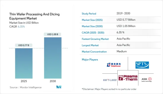
薄晶圆加工和切割设备市场规模预计在 2025 年为 7.7 亿美元,预计到 2030 年将达到 10.5 亿美元,预测期内(2025-2030 年)的复合年增长率为 6.35%。
主要亮点
- 随着电子元件使用量不断增加,人们对电子封装的需求也越来越大,要求电子封装更加资源丰富,以适应各种应用。这些因素正在推动半导体和IC封装市场的成长。
- 预计未来几年推动薄晶圆加工和切割设备需求的主要因素之一是三维积体电路的需求不断增长,3D积体电路广泛应用于记忆卡、智慧型手机、智慧卡和各种运算设备等微型半导体设备。
- 3D电路在一些空间受限的应用中变得越来越普遍,包括便携式消费性电子产品、感测器、MEMS 和工业产品,以提高整体产品性能,包括更快的速度、耐用性、更低的功耗和更轻的记忆体。
- 低成本云端处理解决方案的普及正在推动企业和产业对伺服器和资料中心系统的使用增加,这可能会增加对微处理器和数位讯号处理器等逻辑设备的需求。此外,随着越来越多支援物联网的连接设备的出现,微处理器的使用也增加。这些设备越来越多地使用薄晶圆来实现有效的热管理并提高性能。这些因素正在推动市场成长。
- 多年来,硅晶片一直被用作微电子和 MEMS 的製造平台。绝缘体上硅基基板是标准硅晶片的独特变体。使用约 1-2 μm 厚的二氧化硅键结层将两片晶圆结合在一起,形成晶圆。每个晶圆被平整化至10-50μm的厚度。涂层的具体厚度取决于应用。
- 建造一座最先进的薄晶圆代工厂的成本正在指数级增长,给市场带来压力。近期,半导体製造商的数量正在不断整合。性能改进正在放缓,使得专用薄晶圆更具吸引力。允许薄晶圆通用的设计决策可能并不适用于某些计算任务。
- 半导体研究的各种发展正在为市场创造更多机会。例如,2023年4月,Lapidus正式加入Imec核心合作伙伴计划,在与Imec在先进半导体研究领域的永续合作方面迈出了重要一步。此举加强了该公司对半导体领域长期合作和进步的承诺。
薄晶圆加工切割设备市场趋势
半导体小型化需求的不断增长推动了市场
- 根据美国消费科技协会预测,2022年至2024年间,美国美国电子产品零售额将小幅成长,总额将超过5,000亿美元。预计这将增加开发电子产品对晶圆的需求。与医疗保健和汽车半导体 IC 製造商等其他终端使用者一样,消费性电子产品的需求也迫使 IC 小型化。这将导致市场小型化程度的提高,并有望在预测期内推动需求。
- 从地区来看,无晶圆厂经营模式是亚洲国家在全球半导体销售中占据突出地位的主要因素。无厂半导体公司通常委託製造外包给纯代工厂或外包装组装和测试 (OSAT) 公司。
- FUJIFILM表示,随着人工智慧、物联网、下一代通讯标准「5G」的广泛应用以及自动驾驶技术的进步,对半导体的需求和性能预计会不断提高,半导体设备的小型化仍在继续。这些因素推动了对小型、轻量消费设备的需求,这些设备依靠建立在超薄硅晶片上的3D电路架构来实现最佳效能。
- 这种晶圆极为薄且平坦。同时,小型化也带来了将多种功能整合到单一晶片上的需求。直径12吋的更大晶圆正在引领晶圆技术的新趋势。
- 2023年12月,三星电子与ASML Holding NV宣布将共同投资7.6亿美元在韩国建立先进的研发设施。该设施的主要目的是增强半导体製造工艺,特别注重利用 ASML 的尖端 EUV 技术。这项策略性伙伴关係关係至关重要,因为三星计划在前一年成功量产 3μm 晶片后,到 2025 年实现 2 奈米晶片的商业化。
预计亚太地区将占据最大市场占有率
- 亚太地区是全球最大且成长最快的半导体市场。中国、韩国和新加坡等国家对智慧型手机和其他消费性电子设备的庞大需求促使许多供应商在当地建立製造工厂。
- 中国各市场公司正致力于透过收购和合併来扩大业务。例如,2023年12月,一家中国半导体设计公司与一家马来西亚晶片封装公司合作组装高阶图形处理单元(GPU)。由中国华天科技控股的友尼森公司和其他马来西亚晶片封装公司注意到来自中国合作伙伴的业务和咨询增加。 Xfusion 和 StarFive 等中国公司曾计划在马来西亚扩张。
- 鑑于全球半导体产业不断变化的动态,越南和印度等其他国家也在寻求成为晶片製造服务的替代者。这一转变表明,中国企业选择在海外组装晶片,从而降低了地缘政治风险,并使其更容易进入海外市场。
- 日本是半导体产业不可或缺的一部分,因为它是几家主要製造商和电子产业的所在地。预计政府将调查大型晶片製造商进入该国的可能性。同时,日本企业被视为半导体製造和封装中最关键材料的主要供应商。对于日本供应商而言,日本外汇和高製造成本使得材料价格更高,从而为其他低端应用供应商创造了机会。
- 澳洲的电子製造业正在蓬勃发展,各个终端用户产业越来越多地采用先进设备来影响市场的成长。家电产品的成长主要得益于电视和智慧型手机的销售。
- 2023 年 12 月,雪梨大学奈米研究所推出了一款设计类似乐高积木且频宽更高的新晶片。这种紧凑的硅半导体晶片无缝地结合了电子和光子元件。这项突破性技术显着提高了射频(RF)频宽,并提高了晶片内资讯管理的精度。该晶片利用先进的硅光电技术,能够在宽度不到五毫米的空间内整合各种半导体系统。
- 全自动驾驶汽车的成长轨迹将在很大程度上受到亚太地区因素的影响,包括技术进步、消费者接受全自动驾驶汽车的意愿、定价以及供应商和OEM解决汽车安全关键问题的能力。由于这些因素,汽车和半导体行业不断专注于提高技术、协商原材料价格以及为汽车配备可靠的技术。
薄晶圆加工切割设备产业概况
薄晶圆加工和切割设备市场呈现半固体,仅由 Disco、 Panasonic、Nippon Pulse Motor 和 Taiwan Pulse 马达等少数几家大公司组成。薄晶圆製造製程市场仍面临重大挑战。由于上述因素,新进入者进入市场的速度较慢。然而,市场上企业不断的技术创新和研发努力帮助他们保持竞争优势。因此,市场竞争对手之间的竞争处于中等水平。
- 2024 年 3 月:日立高科技宣布推出新系统 LS9300AD,该系统可检查无图案晶圆的正面和背面是否有颗粒和缺陷。除了使用传统的暗场雷射散射法检测异物和缺陷外,LS9300AD 还配备了新的 DIC(微分干涉对比)检测功能,可以检测浅的、低纵横比的、微小的不均匀缺陷。 LS9300AD采用了传统产品中的晶圆边缘夹持方式和旋转台,可以检查晶圆的正面和背面。
- 2023 年 11 月,康宁将其德国雷射技术业务出售给中国苏州德尔福雷射。在此次交易中,苏州德尔福雷射收购了康宁雷射技术部门的全部股份。
其他福利:
- Excel 格式的市场预测 (ME) 表
- 3个月的分析师支持
目录
第一章 引言
- 研究假设和市场定义
- 研究范围
第二章调查方法
第三章执行摘要
第四章 市场洞察
- 市场概览
- 产业吸引力波特五力分析
- 新进入者的威胁
- 买家的议价能力
- 供应商的议价能力
- 替代品的威胁
- 竞争对手之间的竞争强度
- 产业价值链分析
- COVID-19 的副作用和其他宏观经济因素将如何影响市场
第五章市场动态
- 市场驱动因素
- 对智慧卡、RFID 技术和汽车电源 IC 的需求不断增长
- 半导体小型化需求日益增长
- 市场限制
- 製造挑战
第六章市场区隔
- 依设备类型
- 薄膜装置
- 切割设备
- 刀片切割
- 雷射消熔
- 隐形切割
- 等离子切割
- 按应用
- 记忆体/逻辑 (TSV)
- MEMS元件
- 功率元件
- CMOS影像感测器
- RFID
- 其他的
- 按晶圆厚度
- 750微米
- 120微米
- 50微米
- 按晶圆尺寸
- 4英吋或更小
- 5英寸和6英寸
- 8吋
- 12英吋
- 按地区
- 北美洲
- 欧洲
- 亚洲
- 澳洲和纽西兰
- 拉丁美洲
- 中东和非洲
第七章竞争格局
- 公司简介
- Suzhou Delphi Laser Co. Ltd
- SPTS Technologies Limited
- Plasma-Therm LLC
- Han's Laser Technology Industry Group Co. Ltd
- ASM Laser Separation International(ALSI)BV
- Disco Corporation
- Tokyo Seimitsu Co, Ltd(Accretech)
- Neon Tech Co. Ltd
- Advanced Dicing Technologies Ltd
- Panasonic Corporation
- Hitachi High-Tech Corporation
第八章投资分析
第九章 市场机会与未来趋势
The Thin Wafer Processing And Dicing Equipment Market size is estimated at USD 0.77 billion in 2025, and is expected to reach USD 1.05 billion by 2030, at a CAGR of 6.35% during the forecast period (2025-2030).
Key Highlights
- The increasing efforts to make electronic packaging highly resourceful due to the enormous demand for electronic components owing to amplified usage have made electronic packaging useful in a myriad of applications. These factors are driving the growth of the semiconductor and IC packaging market.
- One of the major factors expected to boost the demand for thin wafer processing and dicing equipment in the coming years is the growing demand for three-dimensional integrated circuits, which are widely used in miniature semiconductor devices such as memory cards, smartphones, smart cards, and various computing devices.
- Three-dimensional circuits are becoming more popular in multiple space-constrained applications, such as portable consumer electronics, sensors, MEMS, and industrial products because they improve overall product performance in terms of speed, durability, low power consumption, and lightweight memory.
- Due to the widespread availability of low-cost cloud computing solutions, the expanding use of server and data center systems across various enterprises and industries is likely to fuel demand for logic devices like microprocessors and digital signal processors. In addition, as the number of IoT-enabled linked devices grows, the utilization of microprocessors also increases. Thin wafers are increasingly employed in these devices to enable effective temperature management and enhance performance. Such factors are responsible for the growth of the market.
- Silicon wafers have long been used as a fabrication platform in microelectronics and MEMS. The silicon-on-insulator substrate is a unique variation of the standard silicon wafer. Two silicon wafers are glued together using a bond layer of silicon dioxide with a thickness of about 1-2 μm to make these wafers. One silicon wafer gets flattened down to 10-50 μm in thickness. The application will determine the exact thickness of the coating.
- The cost of building state-of-the-art thin wafer foundries has increased exponentially, which puts pressure on the market. The number of semiconductor manufacturers has consolidated in recent times. Performance boosts are slowing down, making specialized thin wafers increasingly attractive. The design decisions that enable thin wafers to be universal may be sub-optimal for some computing tasks.
- Various developments in semiconductor research further create opportunities for the market. For instance, in April 2023, Rapidus officially joined Imec's Core Partner Program, marking a significant stride in sustainable collaboration with Imec in advanced semiconductor research. This move reinforced their commitment to long-term collaboration and advancement in the semiconductor domain.
Thin Wafer Processing And Dicing Equipment Market Trends
Increasing Need for Miniaturization of Semiconductors is Expected to Drive the Market
- According to the Consumer Technology Association, in the US, retail sales of consumer electronics were expected to grow marginally between 2022 and 2024, with the total value exceeding USD 500 billion. This would increase the demand for wafers to develop electronic products. The demand for consumer electronics products, along with other end users such as healthcare and automotive semiconductor IC manufacturers, is forcing them to reduce the size of ICs. It has, therefore, given rise to miniaturization in the market, which is expected to experience a surge in its demand during the forecast period.
- Across geographies, the fabless business model is the major contributor to the prominent position of various Asian countries in semiconductor sales worldwide. Fabless firms typically outsource fabrication to pure-play foundries and outsourced assembly and test (OSAT) firms.
- According to Fujifilm, the miniaturization of semiconductor devices continues as the increasing use of AI, IoT, and next-generation communication standard '5G' and the advancement of autonomous driving technology are expected to increase the demand for and performance of semiconductors. The factors mentioned above have led to the rise in demand for small and lightweight consumer devices that rely on 3D circuit architecture built onto ultra-thin silicon wafers in order to perform at peak capacity.
- These wafers are extremely thin and flat. At the same time, miniaturization has resulted in the need to integrate several features on a single chip. Due to large-sized wafers (with a diameter of up to 12 inches), there is a new trend in wafer technology.
- In December 2023, Samsung Electronics and ASML Holding NV announced a collaborative investment of USD 760 million to establish an advanced Research and Development (R&D) facility in South Korea. The primary objective of this facility is to enhance semiconductor manufacturing processes, with a specific focus on utilizing ASML's cutting-edge EUV technology. This strategic partnership is crucial for Samsung's goal of commercializing 2-nanometer chips by 2025, building on the successful mass production of 3 µm chips in the preceding year.
Asia-Pacific is Expected to Hold the Largest Market Share
- The Asia-Pacific is the largest and fastest-growing semiconductor market in the world. Significant demand for smartphones and other consumer electronics devices from countries such as China, the Republic of Korea, and Singapore encourages many vendors to set up regional production establishments.
- China's various market players are focusing on expanding business through acquisitions and mergers. For instance, in December 2023, Chinese semiconductor design companies teamed up with Malaysian chip packaging firms to assemble high-end graphics processing units (GPUs). Unisem, the majority of which is owned by China's Huatian Technology, and other Malaysian chip packaging companies noticed an uptick in business and inquiries from their Chinese partners. Companies like Xfusion and StarFive from China planned to expand their operations in Malaysia.
- Given the changing dynamics in the global semiconductor industry, other countries like Vietnam and India are also trying to become alternatives for chip manufacturing services. This shift shows that Chinese companies are choosing to assemble their chips outside China, reducing geopolitical risks and making it easier to reach markets outside the country.
- Japan occupies an essential position in the semiconductor industry as it is home to several major manufacturers and the electronics industry. The government is expected to investigate the potential for bringing major chip makers into the country. Meanwhile, Japanese organizations are considered significant suppliers of the most critical materials consumed in semiconductor manufacturing and packaging. For Japanese suppliers, Japanese exchange rates and high production costs make materials more expensive and open up opportunities for other suppliers for low-end applications.
- The growing electronics manufacturing sector in Australia and the increasing adoption of advanced devices among various end-user industries influence market growth. The sales of televisions and smartphones have primarily driven the increase in consumer electronics.
- In December 2023, the University of Sydney Nano Institute unveiled a new chip designed like LEGO blocks, featuring improved bandwidth. This compact silicon semiconductor chip smoothly combines electronics with photonic components. The breakthrough will significantly increase radio-frequency (RF) bandwidth and enhance the precision of managing information within the chip. Utilizing advanced silicon photonics technology, the chip has integration capabilities for various semiconductor systems, all within a width of less than 5 millimeters.
- The growth trajectory of fully autonomous automobiles is heavily influenced by factors in Asia-Pacific, including technology advancements, consumer willingness to accept fully automated vehicles, pricing, and suppliers' and OEMs' capacity to address significant concerns about vehicle safety. According to these factors, the automotive and semiconductor industries always concentrate on enhancing technologies, negotiating raw material prices, and combining cars with reliable technology.
Thin Wafer Processing And Dicing Equipment Industry Overview
The market for thin wafer processing and dicing is semi-consolidated and comprises very few major players, such as Disco Corporation, Panasonic Corporation, Nippon, and Pulse Motor Taiwan. The market still faces considerable challenges in the manufacturing processes of thin wafers. The above-mentioned factor has led to a slower entry of new players into the market. Nevertheless, the constant innovations and R&D efforts of market players help maintain a competitive edge. Therefore, competitive rivalry in the market is moderate.
- March 2024: Hitachi High-Tech Corporation announced the launch of the LS9300AD, a new system for inspecting the front and back sides of non-patterned wafer surfaces for particles and defects. In addition to the conventional dark-field laser scattering detection of foreign material and defects, the LS9300AD is equipped with a new DIC (Differential Interference Contrast) inspection function that enables the detection of irregular defects, even shallow, low-aspect microscopic defects. LS9300AD has the wafer edge grip method and rotating stage used in conventional products to enable front and backside wafer inspection.
- November 2023: Corning Inc. sold its German laser technology business to Suzhou Delphi Laser in China. The agreement involved Suzhou Delphi Laser acquiring the complete stake in the division known as Corning Laser Technologies.
Additional Benefits:
- The market estimate (ME) sheet in Excel format
- 3 months of analyst support
TABLE OF CONTENTS
1 INTRODUCTION
- 1.1 Study Assumptions and Market Definition
- 1.2 Scope of the Study
2 RESEARCH METHODOLOGY
3 EXECUTIVE SUMMARY
4 MARKET INSIGHTS
- 4.1 Market Overview
- 4.2 Industry Attractiveness Porter's Five Forces Analysis
- 4.2.1 Threat of New Entrants
- 4.2.2 Bargaining Power of Buyers
- 4.2.3 Bargaining Power of Suppliers
- 4.2.4 Threat of Substitute Products
- 4.2.5 Intensity of Competitive Rivalry
- 4.3 Industry Value Chain Analysis
- 4.4 Impact of COVID-19 Aftereffects and Other Macroeconomic Factors on the Market
5 MARKET DYNAMICS
- 5.1 Market Drivers
- 5.1.1 Increasing Demand for Smart Cards, RFID Technology, and Automotive Power ICs
- 5.1.2 Increasing Need for Miniaturization of Semiconductors
- 5.2 Market Restraint
- 5.2.1 Manufacturing Challenges
6 MARKET SEGMENTATION
- 6.1 By Equipment Type
- 6.1.1 Thinning Equipment
- 6.1.2 Dicing Equipment
- 6.1.2.1 Blade Dicing
- 6.1.2.2 Laser Ablation
- 6.1.2.3 Stealth Dicing
- 6.1.2.4 Plasma Dicing
- 6.2 By Application
- 6.2.1 Memory and Logic (TSV)
- 6.2.2 MEMS Devices
- 6.2.3 Power Devices
- 6.2.4 CMOS Image Sensors
- 6.2.5 RFID
- 6.2.6 Others
- 6.3 By Wafer Thickness
- 6.3.1 750 micrometers
- 6.3.2 120 micrometers
- 6.3.3 50 micrometers
- 6.4 By Wafer Size
- 6.4.1 Less than 4 inches
- 6.4.2 5 inches and 6 inches
- 6.4.3 8 inches
- 6.4.4 12 inches
- 6.5 By Geography
- 6.5.1 North America
- 6.5.2 Europe
- 6.5.3 Asia
- 6.5.4 Australia and New Zealand
- 6.5.5 Latin America
- 6.5.6 Middle East and Africa
7 COMPETITIVE LANDSCAPE
- 7.1 Company Profiles
- 7.1.1 Suzhou Delphi Laser Co. Ltd
- 7.1.2 SPTS Technologies Limited
- 7.1.3 Plasma-Therm LLC
- 7.1.4 Han's Laser Technology Industry Group Co. Ltd
- 7.1.5 ASM Laser Separation International (ALSI) BV
- 7.1.6 Disco Corporation
- 7.1.7 Tokyo Seimitsu Co, Ltd (Accretech)
- 7.1.8 Neon Tech Co. Ltd
- 7.1.9 Advanced Dicing Technologies Ltd
- 7.1.10 Panasonic Corporation
- 7.1.11 Hitachi High-Tech Corporation
8 INVESTMENT ANALYSIS
9 MARKET OPPORTUNITIES AND FUTURE TRENDS
 单晶圆加工设备市场:依製程、晶圆尺寸、技术节点及应用划分-2026年至2032年全球预测晶圆加工设备市场:依设备类型、晶圆尺寸、技术节点和终端用户产业划分-全球预测,2026-2032年
 薄晶圆加工和切割设备市场分析及预测(至2035年):按类型、产品类型、服务、技术、组件、应用、材料类型、製程、最终用户和设备划分
 2026年全球晶圆加工设备市场报告
 晶圆加工设备市场-全球产业规模、份额、趋势、机会、预测:按製程、应用、最终用户、地区和竞争对手划分,2021-2031年
 薄晶圆加工切割设备市场机会、成长要素、产业趋势分析及2026年至2035年预测
 全球晶圆切割服务市场:依材料、尺寸、切割技术与地区划分 - 市场预测与分析 (2026-2035)
 薄砖市场:按产品类型、材料类型、应用和地区划分
 晶圆加工与组装设备市场-2025年至2030年预测雷射开槽设备市场(按雷射类型、操作类型、雷射功率容量、技术、应用和最终用户划分)—2025-2030 年全球预测