


 |
市场调查报告书
商品编码
1644795
晶圆加工和组装设备全球市场:市场占有率分析、行业趋势和统计、成长预测(2025-2030 年)Global Wafer Processing and Assembly Equipment - Market Share Analysis, Industry Trends & Statistics, Growth Forecasts (2025 - 2030) |
||||||
※ 本网页内容可能与最新版本有所差异。详细情况请与我们联繫。
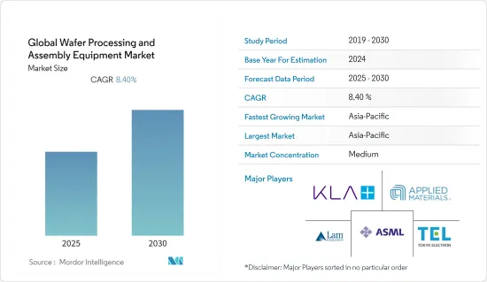
预测期内全球晶圆加工和组装设备市场预计复合年增长率为 8.4%
关键亮点
- 根据印度品牌资产基金会的数据,印度家用电子电器和家用电子电器(ACE) 产业预计将以 9% 的复合年增长率成长,到 2022 年达到 3.15 兆印度卢比(约 483.7 亿美元)。预计到 2024-25 年,印度电子製造业的规模将达到 3,000 亿美元(22.5 兆印度卢比)。此外,预计家用电子电器的使用和消费增加将推动对半导体的需求,从而在整个预测期内推动晶圆加工和组装设备市场的收益。
- 晶圆加工和组装设备行业的一个突出趋势是对更小晶圆和更高设备性能的需求不断增加。例如,晶圆被平坦化到最终几十微米的厚度。用于记忆体、CIS 和电源应用的半导体晶圆大多数都缩小到 100μm 至 200μm 的厚度。对于储存设备而言,需要在单一封装中最大化储存容量,增加资料传输速度和电力消耗(尤其是在行动应用中),这些都推动着对更薄设备的需求。 2D NAND/DRAM 等标准储存设备使用厚度超过 200μm 的晶圆。
- 该地区的政府机构正在计划投资半导体生产,这可能为研究市场创造成长机会。例如,德国经济部于2021年9月宣布,打算向欧盟的「欧洲通用利益重要计划」计画投资30亿欧元。该倡议是欧盟刺激投资和减少进口依赖的主要补贴手段之一。这笔资金将由德国政府用于兴建新的半导体製造厂。这项投资主要是为了减少未来半导体需求对进口半导体的依赖。预计此类政府措施将极大地推动所研究的市场。
- 在晶圆製造週期中,晶圆会因锯切、手动处理、流体喷射、运输系统和拾放设备而受到机械应力。目前商用的功率半导体一般是在200毫米晶圆上製造,厚度为50-100μm,但蓝图显示它们可以做得薄至1μm。机械抛光使这些晶片的背面变薄。研磨痕迹、由于研磨不良而导致的边缘缺口、星形裂纹、由于边缘颗粒卡在研磨中而引起的彗星、嵌入颗粒、解理线和其它各种缺陷都是由抛光过程引起的缺陷。
- 此外,新冠疫情引发的全球半导体晶圆短缺,正促使参与企业集中精力提高产能。例如,中芯国际正制定积极计划,到 2025 年透过在各个城市建设新的晶片製造厂,实现产能翻一番,其中包括 2021 年 9 月宣布将在上海自贸区建立新工厂。
晶圆加工与组装设备市场趋势
薄膜沉淀是市场驱动因素之一
- 化学气相沉积(CVD)技术常用于半导体和薄膜的製造。 CVD设备市场的扩张主要得益于半导体、LED和储存设备产业的快速成长,这是由于对微电子消费品的需求不断增加,以及对Cr6用于电镀的严格限制。
- 2022 年 1 月:韩国专业真空炉製造商 ThermVac Inc. 透过开发可在 900°C 至 2,400°C 温度范围内使用的 CVD 设备的製程技术以及设计和製造技术,继续满足国内外客户的需求。这满足了半导体、光伏、行动电话、航太和国防等高科技产业对耐高温 CVD 组件日益增长的需求。
- 线性溅镀系统用于太阳能、显示器、资料储存和半导体等应用。例如,2021年12月,博世开始量产基于SiC的功率半导体,供应全球汽车製造商。为了满足对半导体日益增长的需求,2021 年,博世位于罗伊特林根的晶圆厂增加了 10,764 平方英尺的无尘室空间。预计到 2023年终将增加 32,292 平方英尺。预计半导体产量的成长将推动所研究市场的发展。
- 预计区域汽车行业的进步将为市场成长创造巨大机会。例如,杜拜最近发起了宣传活动,到 2030 年,该酋长国的道路上将有 42,000 辆电动车。溅镀设备用于涂覆动力传动系统轴承和零件,而电动车新兴市场的发展将成为该市场的主要驱动力。
- 溅镀薄膜在生物医学应用的应用越来越广泛。其中一个例子是采用圆柱形磁控溅镀在一批医疗支架上沉积保护涂层。奈米薄膜广泛应用于电子、纺织、医药、陶瓷和许多其他应用领域。涂有奈米薄膜的织物通常透过化学沉淀、溶胶-凝胶或磁控溅镀方法来生产。例如磁控溅镀具有膜厚可控、纯度高、速度快、温度低、附着力优良、操作简单、环境友善等优点。
亚太地区占市场主要份额
- 亚太地区是全球成长最快的半导体市场。中国、韩国和新加坡等国家对智慧型手机和其他家用电子电器的强劲需求,促使许多供应商在该地区建立生产设施。
- 这些公司正在透过启动新计划来扩大其在该地区的业务,以满足客户的多样化需求。例如,2021 年 9 月,UTAC Holding, Ltd. 在其先进的半导体製造解决方案套件中增加了尖端等离子切割和多计划晶圆 (MPW) 功能。等离子切割可以缩小晶片之间的划线宽度,从而增加每个晶圆上的晶片数量。它还可以实现「近乎完美」的切割质量,不会出现碎片和裂纹,这比可能导致长期侧壁质量问题的传统机械锯切工艺具有明显的优势。
- 此外,上市私人公司都在投资新产品和研发设施。例如,2021 年 9 月,中国最大的晶片代工製造商中芯国际(SMIC)宣布与上海自贸区临港特区达成协议。根据协议,中芯国际将建立一座月产能10万片12吋晶圆的新晶圆厂。中芯国际也于 2021 年 3 月宣布,将与深圳市政府合作,投资 23.5 亿美元建造一座製造工厂,生产 28 奈米(nm)及以上製程的积体电路,月产能为 40,000 片 12 吋晶圆。
- 同样,2021 年 10 月,新南威尔斯州政府意识到全球半导体产业缺乏主要企业,并计划建立一个新中心,以提高该领域关键工作的可行性。该中心名为半导体产业服务局 (S3B),位于雪梨科技中心,由州政府资助。此外,首席科学家和工程师办公室在审查了国内半导体产业后表示,目前澳洲没有以半导体设计或开发为核心业务的大型公司。新工厂将利用该国的晶圆加工和切割设备市场。
- 随着硅通孔(TSV)技术在行动电话和其他无线及网路设备等低功耗、高效能设备中的应用越来越广泛,对隐形切割设备的需求也日益增加。 TSV 允许进行 2.5/3D 封装,使其适用于 TSV 组装/封装(透过隐形切割和其他製程进行晶片到晶片、晶片到晶圆的组装)。对于记忆体和逻辑,采用雷射切割和刀片切割相结合的方式。
晶圆加工与组装设备产业概况
全球晶圆加工和组装设备市场适度整合。为了满足每个行业不断变化的需求,公司倾向于投资创新其产品。此外,参与企业正在采取伙伴关係、合併和收购等策略活动来扩大其影响力。近期市场发展趋势如下:
- 2022年3月-SK siltron宣布在美国密西根州贝城启动碳化硅 (SiC) 半导体晶片製造厂。该公司计划每年生产约6万台。此外,6吋SiC晶圆将成为主力产品。
- 2021 年 9 月-英飞凌科技股份公司将在其位于奥地利的晶圆厂推出一个用于生产 300 毫米薄晶圆上的功率半导体元件的高科技晶片工厂。该投资额达16亿欧元,将成为欧洲微电子领域最大的计划之一。据该公司介绍,该工厂计划的工业半导体年生产能力将足以为其配备光伏系统,总合可产生约 1,500 TWh 的电力,大约是德国年电力消耗量的三倍。
其他福利
- Excel 格式的市场预测 (ME) 表
- 3 个月的分析师支持
目录
第 1 章 简介
- 研究假设和市场定义
- 研究范围
第二章调查方法
第三章执行摘要
第四章 市场洞察
- 市场概况
- 产业吸引力-波特五力分析
- 供应商的议价能力
- 买家的议价能力
- 新进入者的威胁
- 替代品的威胁
- 竞争对手之间的竞争
- 评估新冠肺炎对市场的影响
第五章 市场动态
- 市场驱动因素
- 消费者需求不断成长
电子设备需求不断成长
製造业展望
- 人工智慧的传播
人工智慧、物联网和连网型设备
行业专用设备快速增加
- 市场问题
- 技术的动态本质
生产设备
生产设备
第六章 市场细分
- 依设备类型
- 化学机械抛光
(中国新闻网)
- 蚀刻
- 薄膜沉淀
- CVD
- 溅
- 其他的
- 光阻剂处理
- 组装设备
- 晶粒黏接
- 焊线
- 包装
- 检查和切割
电镀等
- 按地区
- 亚太地区
- 北美洲
- 其他的
- 副产品-晶圆加工设备
- DRAM
- NAND
- 选角/逻辑
- 其他的
第七章:供应商排名分析
第八章 竞争格局
- 公司简介
- Applied Materials Inc
- ASML Holding Semiconductor Company
- Tokyo Electron Limited
- Lam Research Corporation
- KLA Corporation
- Hitachi High-Technologies Corporation
- Disco Corporation
- ASM Pacific Technology
- Kulicke and Soffa Industries, Inc
- BE Semiconductor Industries NV
- Towa Corporation
第九章投资分析
第十章:投资分析市场的未来
The Global Wafer Processing and Assembly Equipment Market is expected to register a CAGR of 8.4% during the forecast period.
Key Highlights
- According to the Indian Brand Equity Foundation, In 2022, the Indian appliance and consumer electronics (ACE) sector is predicted to grow at a 9% compound annual growth rate (CAGR) to INR 3.15 trillion (USD 48.37 billion). The Indian electronics manufacturing sector is expected to reach USD 300 billion (INR 22.5 lakh crore) by 2024-25. Furthermore, increased consumer electronics device usage and consumption are predicted to fuel semiconductor demand, boosting wafer processing and assembly equipment market revenues throughout the projection period.
- A prominent trend in the wafer processing and assembly equipment industry is the growing demand for miniaturized wafers with higher device performance. Wafers, for example, are flattened down to final thicknesses of tens of micrometers. Most semiconductor wafers used in memory, CIS, and power applications are reduced to 100 µm-200 µm in thickness. In the case of memory devices, further thickness reduction is required due to the need to maximize the memory capacity of single packages, increased data transmission rates, and power consumption fueled mostly by mobile applications. Silicon wafers thicker than 200 µm are used in standard memory devices like 2D NAND/DRAM.
- The government bodies in the different regions are planning to invest in the production of semiconductors, which may create an opportunity for the studied market to grow. For instance, in September 2021, Germany's economy ministry stated that the country is willing to invest EUR 3 billion in the EU's "Important Projects of Common European Interest" initiative, which is one of the EU's primary subsidy tools for stimulating investment and reducing import dependency. The money will be used by the German government to build new semiconductor manufacturing factories. This investment is primarily aimed at reducing dependency on imported semiconductors for future semiconductor needs. Government policies like this will significantly drive the studied market.
- Wafers are subjected to mechanical loads induced by sawing, manual handling, liquid jets, transport systems, and pick and place equipment during the wafer manufacturing cycle. Power semiconductors on the market now are generally made on 200-mm wafers with thicknesses ranging from 50 to 100 µm, although their roadmaps allow for wafers as thin as 1 µm. Mechanical polishing thins the backside of these wafers. Grinding marks, grinding failures resulting in edge chips, star cracks, and comets generated by edge particles caught in the grinding wheel, embedded particles, cleavage lines, and a variety of other faults are all defects caused by the polishing process.
- Furthermore, the global shortage of wafer semiconductors led by the COVID-19 pandemic has encouraged players to focus on increasing production capacity. For instance, Semiconductor Manufacturing International Corp (SMIC) has indulged in aggressive plans to double its production capacity by 2025 by constructing new chip fabrication plants in different cities, including its announcement in September 2021 to establish a new factory in Shanghai's free trade zone.
Wafer Processing & Assembly Equipment Market Trends
Thin Film Deposition is One of the Factor Driving the Market
- The Chemical Vapor Deposition (CVD) technology is commonly employed in the fabrication of semiconductors and thin films. The expansion of the CVD equipment market is primarily driven by increasing demand for microelectronics-based consumer items, which is resulting in quicker growth of the semiconductor, LED, and storage device industries, as well as severe limits on the use of Cr6 for electroplating.
- In January 2022, ThermVac Inc., a Korean manufacturer of special vacuum furnaces, continues to respond to the needs of domestic and international clients by developing process technology and design and manufacturing technology for CVD equipment that can be used at temperatures ranging from 900°C to 2,400°C. This corresponds to the growing demand for high-temperature heat-resistant CVD components in high-tech industries like semiconductors, solar power, mobile phones, aerospace, and defense.
- The linear sputtering equipment is used in applications like solar energy, display, Data storage, semiconductor, and many more. For instance, in December 2021, Bosch started the volume production of Sic-based power semiconductors supplying automotive manufacturers worldwide. To meet the increasing demand for such semiconductors, an extra 10,764 square feet were already added to the clean-room space at the Bosch wafer fab in Reutlingen in 2021. Another 32,292 square feet will be added by the end of 2023. Such an increase in the production of semiconductors will drive the studied market.
- The advancements in the regional automotive industry are expected to create significant opportunities for market growth. For instance, Dubai recently launched a campaign to have 42,000 EVs on the streets of Emirates by 2030. The sputtering equipment is used in the coating of Drive train bearings and components as the increase in the developments of EV vehicles will significantly drive the studied market.
- Sputtered thin films are increasingly being used in biomedical applications. An example is a cylindrical magnetron sputtering to deposit protective coatings on batches of medical stents. Nano-films are widely employed in electronics, textiles, pharmaceuticals, ceramics, and various other applications. Fabrics coated with Nanofilm are often created by chemical vapor deposition, sol-gel technique, and magnetron sputtering. The magnetron sputtering method, for example, offers the benefits of controlled film thickness, high purity, high speed and low temperature, excellent adhesion, ease of operation, and environmental friendliness, among others.
Asia Pacific Holds the Major Share of the Market
- Asia-Pacific has the world's fastest-growing semiconductor market. Many vendors are setting up production facilities in the region in response to strong demand for smartphones and other consumer electronics gadgets from nations including China, the Republic of Korea, and Singapore.
- The companies are expanding their presence in the region by starting new projects to cater to the wide need of the customer. For instance, in September 2021, UTAC Holding, Ltd. added state-of-the-art plasma dicing and multi-project wafer (MPW) capabilities to a range of advanced semiconductor manufacturing solutions. Plasma dicing narrows the scribe line width between chips and increases the number of chips per wafer. Also, it provides "nearly perfect" cutting quality with no chips or cracks, which is a clear advantage over traditional mechanical sawing processes that lead to chronic sidewall quality issues.
- Further public agencies and private companies are investing in new products and research & development facilities. For instance, In September 2021, China's largest contract chipmaker Semiconductor Manufacturing International Corp (SMIC) announced the company's agreement with the Lin-Gang Special area-part of Shanghai's free trade zone. This agreement enables SMIC to establish a new foundry with a monthly planned capacity of 100,000 12-inch wafers. Also, in March 2021, the company announced an investment of USD 2.35 billion in coordination with the Shenzhen government for a manufacturing facility to produce 28nanometre (nm) and above integrated circuits with a monthly capacity of 40,000 12-inch wafers.
- Similarly, in October 2021, the Government of New South Wales is aware that the global semiconductor industry lacks Australia's major players and plans a new center to improve the feasibility of critical jobs in this sector. The hub, the Semiconductor Sector Service Bureau (S3B), will be based in Sydney's Tech Central and be funded by the state government. Further, Chief Scientist and Engineer Office, after researching the national semiconductor scene, mentioned there are currently no major Australian companies with semiconductor design or semiconductor development as their core business. The new hub leverages the country's wafer processing and dicing equipment market.
- The demand for stealth dicing equipment is growing as TSV (Through Silicon Via) technology becomes more prevalent for low-power, high-performance devices such as mobile phones and other wireless and networking devices. As TSV can package 2.5/3D for the applications listed above, the equipment is useful for TSV Assembly/Packaging (chip-to-chip and chip-to-wafer assembly with stealth dicing and other processes). In Memory and Logic, a combination of laser dicing and blade dicing is used.
Wafer Processing & Assembly Equipment Industry Overview
The Global Wafer Processing and Assembly Equipment market is moderately consolidated. Players tend to invest in innovating their product offerings to cater to the different industry's changing demands. Moreover, players adopt strategic activities like partnerships, mergers, and acquisitions to expand their presence. Some of the recent developments in the market are:
- March 2022 - SK siltron announced the beginning of the operation of the Silicon carbide (SiC) semiconductor wafer manufacturing plant in Bay City, Michigan, US. The company has a plan to produce around 60,000 annually. Also, a 6-inch SiC wafer is the main product of the company.
- September 2021 - Infineon Technologies AG launched its high-tech chip factory for power semiconductor devices on 300-millimeter thin wafers at its Villach site in Austria. At EUR 1.6 billion, the investment made by the company represents one of the largest such projects in the microelectronics sector in Europe. According to the company, the annual capacity planned for industrial semiconductors from the facility is sufficient to equip solar systems producing a total of around 1,500 TWh of electricity, which is around three times the annual power consumption of Germany.
Additional Benefits:
- The market estimate (ME) sheet in Excel format
- 3 months of analyst support
TABLE OF CONTENTS
1 INTRODUCTION
- 1.1 Study Assumption And Market Defination
- 1.2 Scope of the study
2 RESEARCH METHODOLOGY
3 EXECUTIVE SUMMARY
4 MARKET INSIGHTS
- 4.1 Market Overview
- 4.2 Industry Attractiveness - Porter's Five Forces Analysis
- 4.2.1 Bargaining Power Of Suppliers
- 4.2.2 Bargaining Power Of Buyers
- 4.2.3 Threat Of New Entrants
- 4.2.4 Threat Of Substitutes
- 4.2.5 Intensity Of Competitive Rivalry
- 4.3 Assessment of the Impact of Covid-19 on the Market
5 MARKET DYNAMICS
- 5.1 Market Drivers
- 5.1.1 Increasing Needs of Consumer
Electronic Devices Boosting the
Manufacturing Prospects
- 5.1.2 Proliferation of Artificial
Intelligence, IoT and Connected
Devices across Industry Verticals
- 5.2 Market Challenges
- 5.2.1 Dynamic Nature of Technologies
Requires Several Changes in
Manufacturing Equipment
6 MARKET SEGMENTATION
- 6.1 By Equipment Type
- 6.1.1 Chemical Mechanical Polishing
(CMP)
- 6.1.2 Etching
- 6.1.3 Thin Film Deposition
- 6.1.3.1 CVD
- 6.1.3.2 Sputter
- 6.1.3.3 Other Type
- 6.1.4 Photoresist Processing
- 6.1.5 Assembly Equipment
- 6.1.5.1 Die Attach
- 6.1.5.2 Wire Bonding
- 6.1.5.3 Packaging
- 6.1.5.4 Inspection, Dicing,
Plating and Others
- 6.2 By Geography
- 6.2.1 Asia-Pacific
- 6.2.2 North America
- 6.2.3 Rest of the World
- 6.3 By Product - Wafer Processing Equipment
- 6.3.1 DRAM
- 6.3.2 NAND
- 6.3.3 Foundry/Logic
- 6.3.4 Other Products
7 VENDOR RANKING ANALYSIS
8 COMPETITIVE LANDSCAPE
- 8.1 Company Profiles
- 8.1.1 Applied Materials Inc
- 8.1.2 ASML Holding Semiconductor Company
- 8.1.3 Tokyo Electron Limited
- 8.1.4 Lam Research Corporation
- 8.1.5 KLA Corporation
- 8.1.6 Hitachi High-Technologies Corporation
- 8.1.7 Disco Corporation
- 8.1.8 ASM Pacific Technology
- 8.1.9 Kulicke and Soffa Industries, Inc
- 8.1.10 BE Semiconductor Industries N.V
- 8.1.11 Towa Corporation
9 INVESTMENT ANALYSIS
10 FUTURE OF THE MARKET
 单晶圆加工设备市场:依製程、晶圆尺寸、技术节点及应用划分-2026年至2032年全球预测
 薄晶圆加工和切割设备市场分析及预测(至2035年):按类型、产品类型、服务、技术、组件、应用、材料类型、製程、最终用户和设备划分
 2026年全球晶圆加工设备市场报告
 晶圆加工设备市场-全球产业规模、份额、趋势、机会、预测:按製程、应用、最终用户、地区和竞争对手划分,2021-2031年
 薄晶圆加工切割设备市场机会、成长要素、产业趋势分析及2026年至2035年预测
 全球晶圆切割服务市场:依材料、尺寸、切割技术与地区划分 - 市场预测与分析 (2026-2035)
 薄砖市场:按产品类型、材料类型、应用和地区划分
 晶圆加工与组装设备市场-2025年至2030年预测雷射开槽设备市场(按雷射类型、操作类型、雷射功率容量、技术、应用和最终用户划分)—2025-2030 年全球预测
 薄晶圆加工和切割设备:市场占有率分析、行业趋势和成长预测(2025-2030)