


 |
市场调查报告书
商品编码
1982267
晶圆级封装市场机会、成长要素、产业趋势分析及2026-2035年预测。Wafer Level Packaging Market Opportunity, Growth Drivers, Industry Trend Analysis, and Forecast 2026 - 2035 |
||||||
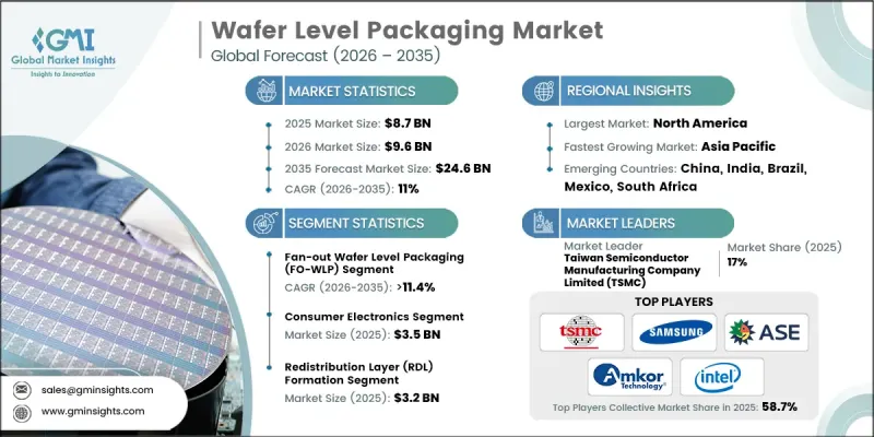
2025年全球晶圆层次电子构装市场价值为87亿美元,预计2035年将以11%的复合年增长率成长至246亿美元。
晶圆层次电子构装是一种先进的半导体製造技术,它在晶圆阶段完成封装,即在晶片分离之前。这种方法支援紧凑的尺寸、高效的散热和多晶片集成,从而提升先进电子系统的性能。随着业界对更高运算能力、能源效率和小型化的需求不断增长,晶圆层次电子构装正成为支撑下一代半导体创新的关键要素。该技术透过简化生产流程,提高了互连密度,改善了讯号完整性,并带来了成本优势。数据驱动型、汽车和连网生态系统对高效能、高整合半导体元件的需求日益增长,正在加速晶圆级封装的普及应用。製造商正在优先考虑可扩展的封装架构,以适应不断演变的复杂设计,同时保持产量比率最佳化和可靠性标准。总而言之,晶圆级封装在全球半导体价值链中正日益占据战略重要地位。
| 市场范围 | |
|---|---|
| 开始年份 | 2025 |
| 预测期 | 2026-2035 |
| 上市时的市场规模 | 87亿美元 |
| 预测金额 | 246亿美元 |
| 复合年增长率 | 11% |
在各个行业中,先进半导体节点的采用率正在迅速提高,以提升装置性能和整合密度。晶圆层次电子构装实现了晶圆级堆迭和先进的互连解决方案,从而支援为新兴连接平台、电动出行系统和资料密集型基础设施开发高可靠性半导体产品。现代半导体应用需要精确的温度控管、更高的产量比率和高密度互连架构,以满足复杂整合的需求。晶圆层次电子构装技术支援扇出结构和麵板级扩充性,为用于先进运算和智慧型系统的3D积体电路和感测器模组提供稳健的堆迭解决方案。晶片组架构、先进的重线路重布、光电相容性以及人工智慧驱动的组装製程的整合进一步提高了封装效率。
扇出型晶圆级封装 (FOWLP) 市场预计在 2025 年达到 36 亿美元,并在 2026 年至 2035 年间以 11.4% 的复合年增长率成长。由于其能够实现更高的输入/输出密度、更短的走线长度以及更优异的电气和热性能,该细分市场占据了晶圆层次电子构装市场最大的份额。其设计适应性和与异质整合架构的兼容性巩固了其在先进半导体製造领域的地位。为了满足不断增长的需求,製造商正致力于开发耐用、高性能的扇出型解决方案,并辅以先进的重线路重布、创新的封装材料和可扩展的面板级加工工具。
预计2025年,线路重布形成领域的市场规模将达32亿美元,主要驱动力是技术进步。该领域的扩张得益于晶片级设计和3D异构整合在复杂度高的半导体应用中的日益普及。线路重布技术能够实现逻辑、记忆体和电源组件之间的高密度互连,从而支援先进的半导体功能并增强系统整合。
预计到2025年,北美晶圆层次电子构装市占率将达到42.6%。该地区的成长主要得益于强劲的半导体研发活动、旨在提升国内製造能力的联邦资助倡议,以及对高效能处理器和先进运算平台日益增长的需求。封装创新和在先进半导体製造领域的领先地位,持续巩固北美在全球市场的主导地位。
目录
第一章:调查方法和范围
第二章执行摘要
第三章业界考察
- 生态系分析
- 供应商情况
- 利润率
- 成本结构
- 每个阶段增加的价值
- 影响价值链的因素
- 中断
- 影响产业的因素
- 促进因素
- 行动和穿戴式装置对小型化的需求日益增长
- 人工智慧加速器和高频宽记忆体的成长
- 汽车电子和ADAS的扩展
- 5G和边缘运算设备的普及
- 人们越来越关注大规模生产中的成本降低问题。
- 产业潜在风险与挑战
- 面板级WLP小型化带来的高昂设备成本
- 超薄晶圆产量比率的技术挑战
- 市场机会
- 采用晶片组架构和先进的SiP技术
- 柔性/混合电子和光电的发展
- 促进因素
- 成长潜力分析
- 监理情势
- 北美洲
- 欧洲
- 亚太地区
- 拉丁美洲
- 中东和非洲
- 波特五力分析
- PESTEL 分析
- 科技与创新趋势
- 当前技术趋势
- 新兴技术
- 新兴经营模式
- 合规要求
- 专利分析
第四章 竞争情势
- 介绍
- 企业市占率分析
- 按地区
- 北美洲
- 欧洲
- 亚太地区
- 拉丁美洲
- 中东和非洲
- 市场集中度分析
- 按地区
- 主要企业的竞争标竿分析
- 财务绩效比较
- 销售量
- 利润率
- 研究与开发
- 产品系列比较
- 产品线
- 科技
- 创新
- 区域扩张比较
- 全球扩张分析
- 服务网路覆盖
- 按地区分類的市场渗透率
- 竞争定位矩阵
- 领导者
- 挑战者
- 追踪者
- 小众玩家
- 战略展望矩阵
- 财务绩效比较
- 2022-2025 年重大发展
- 併购
- 伙伴关係和联盟
- 技术进步
- 业务拓展与投资策略
- 永续发展倡议
- 数位转型计划
- 新兴/Start-Ups竞争对手的发展趋势
第五章 市场估价与预测:依包装技术划分,2022-2035年
- ,
- 晶圆级晶片封装(WLCSP/WL-CSP)
- 扇入式晶圆级封装(FI-WLP)
- 扇出型晶圆级封装(FO-WLP)
第六章 市场估价与预测:依製程划分,2022-2035年
- 线路重布(RDL)形成
- 晶圆凸块
- 晶圆级凸点下金属化(UBM)
- 晶圆级钝化和保护层
- 晶圆减薄和背面研磨
第七章 市场估计与预测:依材料划分,2022-2035年
- RDL材料
- 介电和钝化材料
- 焊料和铜线材料
- 晶圆级封装化合物
第八章 市场估算与预测:依最终用途划分,2022-2035年
- 家用电子电器
- 汽车电子
- 工业电子设备
- 物联网设备
- 通讯设备
- 其他的
第九章 晶圆级封装市场估价与预测:按地区划分,2022-2035年
- 按地区
- 北美洲
- 我们
- 加拿大
- 欧洲
- 英国
- 德国
- 法国
- 义大利
- 西班牙
- 荷兰
- 其他欧洲地区
- 亚太地区
- 中国
- 印度
- 日本
- 韩国
- 澳洲
- 亚太其他地区
- 拉丁美洲
- 巴西
- 墨西哥
- 阿根廷
- 其他拉丁美洲地区
- 中东和非洲(MEA)
- 沙乌地阿拉伯
- 南非
- 阿拉伯聯合大公国
- 其他中东和非洲地区
第十章:公司简介
- Amkor Technology, Inc.
- ASE Technology Holding Co., Ltd.
- China Wafer Level CSP Co., Ltd.
- ChipMOS Technologies Inc.
- Deca Technologies Inc.
- Fujitsu Limited
- HANA Micron Inc.
- Huatian Technology Co., Ltd.
- Intel Corporation
- Jiangsu Changjiang Electronics Technology Co., Ltd.(JCET Group)
- Powertech Technology Inc.(PTI)
- Samsung Electronics Co., Ltd.
- STATS ChipPAC Pte. Ltd.
- Taiwan Semiconductor Manufacturing Company Limited(TSMC)
- Tongfu Microelectronics Co., Ltd.
The Global Wafer Level Packaging Market was valued at USD 8.7 billion in 2025 and is estimated to grow at a CAGR of 11% to reach USD 24.6 billion by 2035.
Wafer level packaging is an advanced semiconductor manufacturing technique that completes the packaging process at the wafer stage before individual chip separation. This approach supports compact form factors, efficient thermal dissipation, and multi-die integration, enabling higher performance across advanced electronic systems. As industries push for greater computing capability, energy efficiency, and miniaturization, wafer level packaging is becoming a critical enabler of next-generation semiconductor innovation. The technology enhances interconnect density, improves signal integrity, and delivers cost advantages through streamlined production. Growing demand for high-performance and highly integrated semiconductor devices across data-driven, automotive, and connected ecosystems is accelerating adoption. Manufacturers are prioritizing scalable packaging architectures that address evolving design complexity while maintaining yield optimization and reliability standards. Overall, wafer level packaging continues to gain strategic importance within the global semiconductor value chain.
| Market Scope | |
|---|---|
| Start Year | 2025 |
| Forecast Year | 2026-2035 |
| Start Value | $8.7 Billion |
| Forecast Value | $24.6 Billion |
| CAGR | 11% |
Industries are rapidly adopting advanced semiconductor nodes to increase device performance and integration density. Wafer level packaging enables wafer-scale stacking and advanced interconnect solutions, supporting the development of high-reliability semiconductor products for emerging connectivity platforms, electrified mobility systems, and data-intensive infrastructure. Modern semiconductor applications require precise thermal management, enhanced yield performance, and dense interconnect architectures to meet complex integration demands. Wafer level packaging technologies support fan-out structures and panel-level scalability, enabling robust stacking solutions for three-dimensional integrated circuits and sensor modules used in advanced computing and intelligent systems. The integration of chiplet architectures, sophisticated redistribution layers, photonics compatibility, and AI-assisted assembly processes is further enhancing packaging efficiency.
The fan-out wafer level packaging segment was valued at USD 3.6 billion in 2025 and is estimated to grow at a CAGR of 11.4% during 2026-2035. This segment holds the largest share of the wafer level packaging market due to its ability to deliver higher input/output density, reduced interconnect length, and improved electrical and thermal performance. Its design adaptability and compatibility with heterogeneous integration architectures have strengthened its position in advanced semiconductor manufacturing. To address rising demand, manufacturers are focusing on durable, high-performance fan-out solutions supported by advanced redistribution layers, innovative molding materials, and scalable panel-level processing tools.
The redistribution layer formation segment generated USD 3.2 billion in 2025, leading the market by technology. This segment is expanding due to the increasing adoption of chiplet-based designs and three-dimensional heterogeneous integration in high-complexity semiconductor applications. Redistribution layer technology enables high-density interconnections between logic, memory, and power components, supporting advanced semiconductor functionality and enhanced system integration.
North America Wafer Level Packaging Market accounted for 42.6% share in 2025. Regional growth is driven by substantial semiconductor research and development activity, federal funding initiatives aimed at strengthening domestic fabrication capacity, and increasing demand for high-performance processors and advanced computing platforms. Leadership in packaging innovation and advanced semiconductor manufacturing continues to reinforce North America's dominant position within the global market.
Major companies operating in the Global Wafer Level Packaging Market include Taiwan Semiconductor Manufacturing Company Limited, Intel Corporation, Samsung Electronics Co., Ltd., ASE Technology Holding Co., Ltd., Amkor Technology, Inc., Jiangsu Changjiang Electronics Technology Co., Ltd., Powertech Technology Inc., Tongfu Microelectronics Co., Ltd., Huatian Technology Co., Ltd., ChipMOS Technologies Inc., China Wafer Level CSP Co., Ltd., HANA Micron Inc., STATS ChipPAC Pte. Ltd., Fujitsu Limited, and Deca Technologies Inc.. Companies competing in the Global Wafer Level Packaging Market are strengthening their competitive position through sustained investment in advanced packaging research and process innovation. Leading players are expanding panel-level manufacturing capabilities and developing next-generation redistribution layer technologies to improve integration density and thermal performance. Strategic collaborations with semiconductor foundries and system designers are enabling co-development of customized packaging architectures. Firms are also investing in automation, AI-driven inspection systems, and yield optimization tools to enhance production efficiency. Geographic expansion into emerging semiconductor hubs and capacity upgrades in advanced packaging facilities are supporting long-term growth.
Table of Contents
Chapter 1 Methodology and Scope
- 1.1 Market scope and definition
- 1.2 Research design
- 1.2.1 Research approach
- 1.2.2 Data collection methods
- 1.3 Data mining sources
- 1.3.1 Global
- 1.3.2 Regional/Country
- 1.4 Base estimates and calculations
- 1.4.1 Base year calculation
- 1.4.2 Key trends for market estimation
- 1.5 Primary research and validation
- 1.5.1 Primary sources
- 1.6 Forecast model
- 1.7 Research assumptions and limitations
Chapter 2 Executive Summary
- 2.1 Industry snapshot
- 2.2 Key market trends
- 2.2.1 Packaging type trends
- 2.2.2 Process trends
- 2.2.3 Material trends
- 2.2.4 End-use application trends
- 2.2.5 Regional trends
- 2.3 TAM Analysis, 2026-2035 (USD Billion)
- 2.4 CXO perspectives: Strategic imperatives
Chapter 3 Industry Insights
- 3.1 Industry ecosystem analysis
- 3.1.1 Supplier Landscape
- 3.1.2 Profit Margin
- 3.1.3 Cost structure
- 3.1.4 Value addition at each stage
- 3.1.5 Factor affecting the value chain
- 3.1.6 Disruptions
- 3.2 Industry impact forces
- 3.2.1 Growth drivers
- 3.2.1.1 Rising demand for miniaturization in mobile and wearables
- 3.2.1.2 Growth in AI accelerators and high-bandwidth memory
- 3.2.1.3 Expansion of automotive electronics and ADAS
- 3.2.1.4 Proliferation of 5G and edge computing devices
- 3.2.1.5 Increasing focus on cost reduction in high-volume production
- 3.2.2 Industry pitfalls and challenges
- 3.2.2.1 High equipment costs for panel-level WLP scaling
- 3.2.2.2 Technical challenges in yield for ultra-thin wafers
- 3.2.3 Market opportunities
- 3.2.3.1 Adoption of chiplet architectures and advanced SiPs
- 3.2.3.2 Growth in flexible/hybrid electronics and photonics
- 3.2.1 Growth drivers
- 3.3 Growth potential analysis
- 3.4 Regulatory landscape
- 3.4.1 North America
- 3.4.2 Europe
- 3.4.3 Asia Pacific
- 3.4.4 Latin America
- 3.4.5 Middle East & Africa
- 3.5 Porter's analysis
- 3.6 PESTEL analysis
- 3.7 Technology and innovation landscape
- 3.7.1 Current technological trends
- 3.7.2 Emerging technologies
- 3.8 Emerging business models
- 3.9 Compliance requirements
- 3.10 Patent analysis
Chapter 4 Competitive Landscape, 2025
- 4.1 Introduction
- 4.2 Company market share analysis
- 4.2.1 By Region
- 4.2.1.1 North America
- 4.2.1.2 Europe
- 4.2.1.3 Asia Pacific
- 4.2.1.4 Latin America
- 4.2.1.5 Middle East & Africa
- 4.2.2 Market Concentration Analysis
- 4.2.1 By Region
- 4.3 Competitive benchmarking of key players
- 4.3.1 Financial performance comparison
- 4.3.1.1 Revenue
- 4.3.1.2 Profit margin
- 4.3.1.3 R&D
- 4.3.2 Product portfolio comparison
- 4.3.2.1 Product range breadth
- 4.3.2.2 Technology
- 4.3.2.3 Innovation
- 4.3.3 Geographic presence comparison
- 4.3.3.1 Global footprint analysis
- 4.3.3.2 Service network coverage
- 4.3.3.3 Market penetration by region
- 4.3.4 Competitive positioning matrix
- 4.3.4.1 Leaders
- 4.3.4.2 Challengers
- 4.3.4.3 Followers
- 4.3.4.4 Niche players
- 4.3.5 Strategic outlook matrix
- 4.3.1 Financial performance comparison
- 4.4 Key developments, 2022-2025
- 4.4.1 Mergers and acquisitions
- 4.4.2 Partnerships and collaborations
- 4.4.3 Technological advancements
- 4.4.4 Expansion and investment strategies
- 4.4.5 Sustainability initiatives
- 4.4.6 Digital transformation initiatives
- 4.5 Emerging/ startup competitors landscape
Chapter 5 Market Estimates & Forecast, By Packaging Technology, 2022 - 2035 (USD Million)
- 5.1 Key trends,
- 5.2 Wafer-Level Chip Scale Packaging (WLCSP / WL-CSP)
- 5.3 Fan-In Wafer Level Packaging (FI-WLP)
- 5.4 Fan-Out Wafer Level Packaging (FO-WLP)
Chapter 6 Market Estimates and Forecast, By Process, 2022 - 2035 (USD Million)
- 6.1 Key trends
- 6.2 Redistribution Layer (RDL) formation
- 6.3 Wafer bumping
- 6.4 Wafer-level under-bump metallization (UBM)
- 6.5 Wafer-level passivation and protection layers
- 6.6 Wafer thinning and back grinding
Chapter 7 Market Estimates and Forecast, By Materials, 2022 - 2035 (USD Million)
- 7.1 Key trends
- 7.2 RDL materials
- 7.3 Dielectric and passivation materials
- 7.4 Solder and copper interconnect materials
- 7.5 Wafer-level encapsulation compounds
Chapter 8 Market Estimates and Forecast, By End-use Application, 2022 - 2035 (USD Million)
- 8.1 Key trends
- 8.2 Consumer electronics
- 8.3 Automotive electronics
- 8.4 Industrial electronics
- 8.5 IoT devices
- 8.6 Telecommunications devices
- 8.7 Others
Chapter 9 Wafer level packaging Market Estimates & Forecast, By Region, 2022 - 2035 (USD Million)
- 9.1 Key trends, by region
- 9.2 North America
- 9.2.1 U.S.
- 9.2.2 Canada
- 9.3 Europe
- 9.3.1 UK
- 9.3.2 Germany
- 9.3.3 France
- 9.3.4 Italy
- 9.3.5 Spain
- 9.3.6 Netherlands
- 9.3.7 Rest of Europe
- 9.4 Asia-Pacific
- 9.4.1 China
- 9.4.2 India
- 9.4.3 Japan
- 9.4.4 South Korea
- 9.4.5 Australia
- 9.4.6 Rest of Asia-Pacific
- 9.5 Latin America
- 9.5.1 Brazil
- 9.5.2 Mexico
- 9.5.3 Argentina
- 9.5.4 Rest of Latin America
- 9.6 MEA
- 9.6.1 Saudi Arabia
- 9.6.2 South Africa
- 9.6.3 UAE
- 9.6.4 Rest of MEA
Chapter 10 Company Profiles
- 10.1 Amkor Technology, Inc.
- 10.2 ASE Technology Holding Co., Ltd.
- 10.3 China Wafer Level CSP Co., Ltd.
- 10.4 ChipMOS Technologies Inc.
- 10.5 Deca Technologies Inc.
- 10.6 Fujitsu Limited
- 10.7 HANA Micron Inc.
- 10.8 Huatian Technology Co., Ltd.
- 10.9 Intel Corporation
- 10.10 Jiangsu Changjiang Electronics Technology Co., Ltd. (JCET Group)
- 10.11 Powertech Technology Inc. (PTI)
- 10.12 Samsung Electronics Co., Ltd.
- 10.13 STATS ChipPAC Pte. Ltd.
- 10.14 Taiwan Semiconductor Manufacturing Company Limited (TSMC)
- 10.15 Tongfu Microelectronics Co., Ltd.
 晶圆级封装市场预测至2034年-全球分析(依封装技术、互连技术、材料类型、晶圆尺寸、装置类型、应用、最终使用者和地区划分)
 晶圆级製造设备市场:依设备类型、晶圆尺寸及应用划分-2026-2032年全球市场预测晶圆级可靠性测试设备市场:按测试类型、设备类型、最终用户产业、二维、技术节点和晶圆尺寸划分 - 全球预测 2026-2032晶圆级点胶设备市场:按技术、自动化程度、设备类型、应用和最终用户产业划分 - 全球预测(2026-2032年)非製冷晶圆级封装检测器市场(按检测器类型、像素间距、检测器解析度、最终用户和应用划分)-全球预测,2026-2032年
 晶圆级封装市场规模、份额、趋势及预测(按封装技术、最终用途产业和地区),2025 年至 2033 年
 晶圆级製造设备市场,2025 年至 2029 年至 2030 年晶圆层次电子构装市场预测:按封装类型、互连技术、最终用户和地区分類的全球分析
 晶圆级製造设备市场,按类型、应用、最终用户、国家和地区 - 2024-2032 年行业分析、市场规模、市场份额和预测
 全球晶圆製造设备市场