


 |
市场调查报告书
商品编码
1936014
全球旋涂碳(SOC)市场按类型、应用和最终用户划分-预测至2032年Spin-on Carbon Market by Type (Hot-Temperature, Normal-Temperature), Application (Logic Devices, Memory Devices, Power Devices, MEMS, Photonics, Advanced Packaging), and End User (Foundries, IDMs & OSAT Vendors) - Global Forecast to 2032 |
||||||
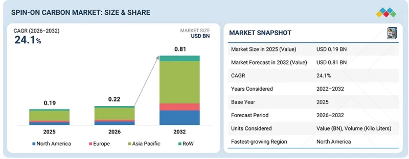
全球旋涂碳(SOC)市场预计将从 2026 年的 2.2 亿美元成长到 2032 年的 8.1 亿美元,在此期间的复合年增长率为 24.1%。
这一成长将受到极紫外线 (EUV)微影术和深紫外线 (DUV) 多重图形化技术日益普及的推动。
| 调查范围 | |
|---|---|
| 调查期 | 2021-2032 |
| 基准年 | 2024 |
| 预测期 | 2025-2032 |
| 单元 | 10亿美元 |
| 部分 | 类型、用途、最终用户、区域 |
| 目标区域 | 北美、欧洲、亚太地区及其他地区 |
旋涂碳(SOC)可改善图案转移性能,最大限度地减少线崩坏,并提高大批量半导体製造的产量比率。 SOC 可提供均匀的薄膜厚度和优异的机械性能,这对于在日益缩小的製程节点上保持製程可靠性至关重要。
“从终端用户来看,预计到 2032 年,晶圆代工厂领域将占据最大的市场份额。”
预计到2032年,晶圆代工厂代工将成为旋涂碳(SOC)市场最大的份额。这主要归功于晶圆代工厂在大规模半导体製造中的关键作用以及先进製程技术的快速普及。台积电、三星晶圆代工和格罗方德等领先的晶圆代工厂服务于包括逻辑电路、记忆体介面、人工智慧加速器和汽车半导体在内的多元化基本客群。这种广泛的覆盖范围使得晶圆开片量远高于其他终端用户,直接转化为在各种微影术和蚀刻层中对SOC材料的持续和重复消耗。此外,晶圆代工厂在极微影术和复杂的深紫外线多重图形化技术的应用方面处于领先地位,而SOC对于提高图形转移精度、减少线崩坏以及产量比率至关重要。随着向更小节点(例如5nm和3nm)的过渡不断推进,更小的关键尺寸和更多的製程步骤将进一步提高每片晶圆的SOC用量。此外,晶圆代工厂正在加大对先进封装技术的投入,例如晶圆基板晶片封装(CoWoS)、整合式扇出封装(InFO)和3D整合。这些製程需要旋涂碳(SOC)用于平坦化和层间绝缘。亚太地区、北美和欧洲产能的持续扩张预计将推动长期需求。因此,预计到2030年,晶圆代工厂将成为旋涂碳(SOC)的最大消费者。
“从应用领域来看,预计先进封装领域在预测期内将实现最高的复合年增长率。”
随着半导体製造快速朝向高密度和异构整合方向发展,旋涂碳(SOC)市场的先进封装领域预计将在预测期内实现最高的复合年增长率。扇出型晶圆级封装(FOWLP)、2.5D/3D积体电路(IC)、晶片组和硅穿孔电极(TSV)等技术需要优异的平坦化、强层间黏附性和精确的图案转移能力,而旋涂碳(SOC)材料恰好能够满足这些需求。随着装置结构日益复杂,每个封装所需的旋涂碳(SOC)用量预计将会增加,从而实现比传统前端应用更快的量产速度。此外,高效能运算(HPC)、人工智慧(AI)加速器和资料中心处理器需求的不断增长,也推动了先进封装解决方案的应用,以克服电晶体级尺寸缩放的限制。旋涂碳(SOC)材料对于控制细间距互连和减少多层製程的缺陷至关重要。市场扩张也得益于封装外包给OSAT公司的趋势日益增长,这些公司越来越多地使用旋涂碳(SOC)来提高产量比率和生产效率。此外,汽车和5G应用领域封装技术的进步,对高可靠性和热稳定性提出了更高的要求,也推动了旋涂碳(SOC)材料的应用。
本报告研究了全球旋涂碳(SOC)市场,并深入分析了关键驱动因素和限制因素、产品开发和创新以及竞争格局。
目录
第一章 引言
第二章执行摘要
第三章 主要发现
- 旋涂碳(SOC)市场对企业而言极具吸引力的机会
- 旋涂碳(SOC)市场按类型划分
- 按应用分類的旋涂碳(SOC)市场
- 按最终用户分類的旋涂碳(SOC)市场
- 亚太地区旋涂碳(SOC)市场按最终用户和国家划分
- 按地区分類的旋涂碳(SOC)市场
第四章 市场概览
- 市场动态
- 司机
- 抑制因素
- 机会
- 任务
- 相互关联的市场与跨产业机会
- 一级/二级/三级公司的策略性倡议
第五章 产业趋势
- 波特五力分析
- 宏观经济展望
- GDP趋势与预测
- 全球微影术产业趋势
- 全球逻辑装置产业趋势
- 价值链分析
- 生态系分析
- 定价分析
- 主要企业旋涂碳(SOC)价格区间(2024 年)
- 旋涂碳(SOC)平均售价区域趋势(2022-2025)
- 贸易分析
- 进口方案(HS编码381800)
- 出口方案(HS编码381800)
- 重大会议和活动(2026-2027)
- 影响客户业务的趋势/颠覆性因素
- 投资与资金筹措情境(2023-2025 年)
- 案例研究分析
- 2025年美国关税的影响-旋装碳(SOC)市场
- 主要关税税率
- 价格影响分析
- 国家/地区影响力
- 最终用户影响
第六章:技术进步、人工智慧的影响、专利与创新
- 主要新技术
- SOC聚合物配方
- 旋涂工艺控制
- 耐蚀刻片上系统平台
- 互补技术
- 极微影术
- 化学机械抛光(CMP)/抛光液
- 邻近技术
- 旋涂介电材料(SOD)、旋涂玻璃(SOG)
- 原子层沉积(ALD)硬掩模
- 技术蓝图
- 专利分析
- 人工智慧对旋涂碳(SOC)市场的影响
- 主要应用案例和市场潜力
- 来自旋涂碳(SOC)市场企业的最佳实践
- 人工智慧在旋涂碳(SOC)市场应用案例研究
- 相互关联的生态系统及其对市场公司的影响
- 客户对采用人工智慧整合旋涂碳(SOC)的准备情况
第七章:监理环境
- 地方法规和合规性
- 监管机构、政府机构和其他组织
- 业界标准
第八章:顾客状况与购买行为
- 决策流程
- 参与采购流程和评估标准的关键相关利益者
- 采购过程中的关键相关利益者
- 采购标准
- 招募障碍和内部挑战
- 各类终端用户的未满足需求
9. 按类型分類的旋涂碳(SOC)市场
- 高温
- 室温
第十章 依应用分類的旋涂碳(SOC)市场
- 逻辑装置
- 储存装置
- 功率元件
- MEMS
- 光电
- 先进包装
第十一章 以最终用户分類的旋涂碳(SOC)市场
- 晶圆代工厂
- IDMS/OSAT供应商
第十二章 按地区分類的旋涂碳(SOC)市场
- 北美洲
- 我们
- 加拿大
- 墨西哥
- 欧洲
- 英国
- 德国
- 法国
- 其他欧洲
- 亚太地区
- 中国
- 日本
- 韩国
- 台湾
- 亚太其他地区
- 其他地区
- 南美洲
- 中东和非洲
第十三章 竞争格局
- 概述
- 主要参与企业的策略/优势(2021-2025)
- 市占率分析(2025 年)
- 收入分析(2020-2024)
- 公司估值和财务指标
- 品牌和产品比较
- 企业评估矩阵:主要企业(2025 年)
- 公司评估矩阵:Start-Ups/中小企业(2025 年)
- 竞争场景
第十四章:公司简介
- 主要企业
- SAMSUNG SDI
- SHIN-ETSU CHEMICAL CO., LTD.
- DONGJIN SEMICHEM CO LTD
- MERCK KGAA
- YCCHEM CO., LTD.
- BREWER SCIENCE, INC.
- JSR MICRO, INC.
- IRRESISTIBLE MATERIALS LTD
- KOYJ CO., LTD
- NANO-C
- 其他公司
- SK ECOPLANT CO., LTD.
- PIBOND OY
- QNITY ELECTRONICS, INC.
- APPLIED MATERIALS, INC.
- MICROCHEM
- TOKYO ELECTRON LIMITED
- ENTEGRIS
- EV GROUP(EVG)
- TAIWAN SEMICONDUCTOR MANUFACTURING COMPANY LIMITED
- GLOBALFOUNDRIES
- INTEL CORPORATION
- DOW
- BASF
- MITSUBISHI CHEMICAL GROUP CORPORATION
- FUJIFILM WAKO PURE CHEMICAL CORPORATION
第十五章调查方法
第十六章附录
The spin-on carbon market is projected to grow from USD 0.22 billion in 2026 to USD 0.81 billion by 2032 at a compound annual growth rate (CAGR) of 24.1% during this period. This growth is driven by the increasing adoption of extreme ultraviolet (EUV) lithography and complex deep ultraviolet (DUV) multi-patterning techniques.
| Scope of the Report | |
|---|---|
| Years Considered for the Study | 2021-2032 |
| Base Year | 2024 |
| Forecast Period | 2025-2032 |
| Units Considered | Value (USD Billion) |
| Segments | By Type, Application, End User and Region |
| Regions covered | North America, Europe, APAC, RoW |
Spin-on carbon (SOC) enhances pattern transfer performance, minimizes line collapse, and improves yield in high-volume semiconductor manufacturing. SOC is essential for maintaining process reliability in increasingly scaled-down nodes, as it provides uniform film thickness and superior mechanical properties.
"By end user, the foundries segment is projected to account for the largest market share in 2032."
The foundries segment is projected to account for the largest market share in the spin-on carbon market by 2032, primarily due to the crucial role of foundries in high-volume semiconductor manufacturing and the rapid adoption of advanced process technologies. Leading foundries like TSMC, Samsung Foundry, and GlobalFoundries cater to a diverse customer base that includes logic, memory interfaces, AI accelerators, and automotive semiconductors. This broad reach results in significantly higher wafer starts than other end users, which directly translates into consistent and recurring consumption of spin-on carbon materials across various lithography and etch layers. Additionally, foundries are at the forefront of implementing EUV lithography and complex DUV multi-patterning, where spin-on carbon is essential for improving pattern transfer fidelity, reducing line collapse, and enhancing yield at advanced nodes. The ongoing migration to smaller nodes, such as 5 nm and 3 nm, further increases spin-on carbon usage per wafer due to tighter critical dimensions and additional processing steps. Moreover, foundries are enhancing their advanced packaging capabilities, including Chip-on-Wafer-on-Substrate (CoWoS), Integrated Fan-Out (InFO), and 3D integration. These processes require spin-on carbon for planarization and interlayer applications. The ongoing capacity expansions across Asia Pacific, North America, and Europe are expected to boost long-term demand. As a result, foundries are projected to become the largest consumers of spin-on carbon by 2030.
"By application, the advanced packaging segment is projected to record the highest CAGR during the forecast period."
The advanced packaging segment is projected to experience the highest compound annual growth rate (CAGR) in the spin-on carbon market during the forecast period due to the rapid transition toward high-density, heterogeneous integration in semiconductor manufacturing. Technologies such as fan-out wafer-level packaging (FOWLP), 2.5D/3D integrated circuits (ICs), chiplets, and through-silicon vias (TSVs) necessitate superior planarization, strong interlayer adhesion, and precise pattern transfer-capabilities made possible by spin-on carbon materials. As device architectures become more complex, the usage of spin-on carbon per package increases, leading to faster volume growth compared to conventional front-end applications. Furthermore, the rising demand for high-performance computing, AI accelerators, and data center processors drives the adoption of advanced packaging solutions to overcome scaling limitations at the transistor level. Spin-on carbon materials are crucial for managing fine-pitch interconnects and reducing defects during multilayer processing. The growing trend of outsourcing packaging to outsourced semiconductor assembly and test (OSAT) companies also supports market expansion, as these vendors increasingly utilize spin-on carbon to enhance yield and throughput. Additionally, advancements in packaging technologies for automotive and 5G applications, which require high reliability and thermal stability, further promote the adoption of spin-on carbon materials.
"North America is projected to grow at the highest CAGR during the forecast period."
North America is projected to experience the highest compound annual growth rate (CAGR) in the spin-on carbon market, driven by increasing investments in domestic semiconductor manufacturing and advanced packaging infrastructure. The region is seeing substantial construction and expansion of semiconductor fabs, motivated by government incentives, reshoring initiatives, and efforts to localize supply chains. Major foundries and integrated device manufacturers (IDMs) are expanding their capacities for advanced-node and specialty processes, which is directly boosting the demand for spin-on carbon materials in various steps, including lithography, etching, and planarization. Furthermore, North America serves as a key center for innovation in extreme ultraviolet (EUV) lithography, artificial intelligence (AI)-focused processors, and high-performance computing-all of which require high-performance spin-on carbon formulations to achieve optimal yield and pattern fidelity at scaled nodes. Additionally, the rapid advancement of packaging technologies, including 2.5D/3D integration and chiplet-based architectures, is leading to an increased consumption of spin-on carbon per wafer and package. Strong collaboration among material suppliers, equipment manufacturers, and semiconductor producers is facilitating a quick qualification and adoption of next-generation spin-on carbon materials. To summarize, the expansion of fabrication capacity, technological leadership, and the rising demand for advanced semiconductor devices position North America as the fastest-growing regional market for spin-on carbon during the forecast period.
Extensive primary interviews were conducted with key industry experts in the spin-on carbon sector to determine and verify the market size for various segments and subsegments, which were gathered through secondary research.
The breakdown of primary participants is provided below.
- By Company Type: Tier 1 - 40%, Tier 2 - 35%, and Tier 3 - 25%
- By Designation: Directors-20%, Managers - 35%, and Others - 45%
- By Region: Asia Pacific - 40%, Europe - 20%, North America - 30%, and RoW - 10%
The report profiles key players in the spin-on carbon market with their respective market ranking analysis. Prominent players profiled in this report are SAMSUNG SDI (South Korea), Shin-Etsu Chemical Co., Ltd. (Japan), DONGJIN SEMICHEM CO LTD. (South Korea), Merck KGaA (Germany), YCCHEM Co., Ltd. (South Korea), Brewer Science, Inc. (US), JSR Micro, Inc. (US), Irresistible Materials (UK), KOYJ CO., LTD. (South Korea), Nano-C (US), among others.
Additionally, SK ecoplant CO., LTD. (South Korea), Pibond Oy (Finland), Qnity Electronics, Inc. (US), Applied Materials, Inc. (US), MicroCHEM (India), Tokyo Electron Limited (Japan), Entegris (US), EV Group (EVG) (Austria), Taiwan Semiconductor Manufacturing Company Limited (Taiwan), GlobalFoundries (US), Intel Corporation (US), among others, are among the few other companies in the spin-on carbon market.
Research Coverage:
This research report categorizes the spin-on carbon market based on type, application, end user, and region. It describes the major drivers, restraints, challenges, and opportunities pertaining to the spin-on carbon market and forecasts the same till 2032. Additionally, the report includes leadership mapping and analysis of all the companies included in the spin-on carbon market ecosystem.
Key Benefits of Buying the Report:
The report will help the market leaders/new entrants in this market with information on the closest approximations of the numbers for the overall spin-on carbon market and the subsegments. It will also help stakeholders understand the competitive landscape and gain more insights to position their businesses better and plan suitable go-to-market strategies. The report will also help stakeholders understand the pulse of the market and provide them with information on key market drivers, restraints, challenges, and opportunities.
The report provides insights into the following pointers:
- Analysis of key drivers (Rapid advancements in semiconductor manufacturing technologies), restraints (Availability of substitute materials), opportunities (Heightened focus on miniaturization of electronic devices), and challenges (Issues selecting suitable SoC materials for integrated circuit manufacturing) of the spin-on carbon market
- Product Development/Innovation: Detailed insights into upcoming technologies, research & development activities, and product & service launches in the spin-on carbon market
- Market Development: Comprehensive information about lucrative markets across varied regions
- Market Diversification: Exhaustive information about new products & services, untapped geographies, recent developments, and investments in the spin-on carbon market
- Competitive Assessment: In-depth assessment of market share, growth strategies, and service offerings of leading players, such as SAMSUNG SDI (South Korea), Shin-Etsu Chemical Co., Ltd. (Japan), DONGJIN SEMICHEM CO LTD. (South Korea), Merck KGaA (Germany), YCCHEM Co., Ltd. (South Korea), in the spin-on carbon market
TABLE OF CONTENTS
1 INTRODUCTION
- 1.1 STUDY OBJECTIVES
- 1.2 MARKET DEFINITION
- 1.3 STUDY SCOPE
- 1.3.1 MARKETS COVERED AND REGIONAL SCOPE
- 1.3.2 INCLUSIONS AND EXCLUSIONS
- 1.3.3 YEARS CONSIDERED
- 1.4 CURRENCY CONSIDERED
- 1.5 UNIT CONSIDERED
- 1.6 LIMITATIONS
- 1.7 STAKEHOLDERS
- 1.8 SUMMARY OF CHANGES
2 EXECUTIVE SUMMARY
- 2.1 MARKET HIGHLIGHTS AND KEY INSIGHTS
- 2.2 KEY MARKET PARTICIPANTS: MAPPING OF STRATEGIC DEVELOPMENTS
- 2.3 DISRUPTIONS SHAPING SPIN-ON CARBON MARKET
- 2.4 HIGH-GROWTH SEGMENTS
- 2.5 SNAPSHOT: GLOBAL MARKET SIZE, GROWTH RATE, AND FORECAST
3 PREMIUM INSIGHTS
- 3.1 ATTRACTIVE OPPORTUNITIES FOR PLAYERS IN SPIN-ON CARBON MARKET
- 3.2 SPIN-ON CARBON MARKET, BY TYPE
- 3.3 SPIN-ON CARBON MARKET, BY APPLICATION
- 3.4 SPIN-ON CARBON MARKET, BY END USER
- 3.5 SPIN-ON CARBON MARKET IN ASIA PACIFIC, BY END USER AND COUNTRY
- 3.6 SPIN-ON CARBON MARKET, BY GEOGRAPHY
4 MARKET OVERVIEW
- 4.1 INTRODUCTION
- 4.2 MARKET DYNAMICS
- 4.2.1 DRIVERS
- 4.2.1.1 Rapid advances in semiconductor manufacturing technologies
- 4.2.1.2 Increasing need for advanced electronic device packaging
- 4.2.1.3 Growing preference for EUV lithography-enabled memory production
- 4.2.1.4 Rising structural complexity of semiconductor devices
- 4.2.2 RESTRAINTS
- 4.2.2.1 Availability of substitute materials
- 4.2.2.2 High sensitivity of SoC materials to process variations
- 4.2.3 OPPORTUNITIES
- 4.2.3.1 Heightened focus on miniaturization of electronic devices
- 4.2.3.2 Requirement for next-generation memory devices in emerging technologies
- 4.2.3.3 Increase in wafer fabrication capacity
- 4.2.4 CHALLENGES
- 4.2.4.1 Issues in selecting suitable SoC materials for integrated circuit manufacturing
- 4.2.4.2 Challenges in scaling SoC materials for next-generation advanced semiconductor nodes
- 4.2.1 DRIVERS
- 4.3 INTERCONNECTED MARKETS AND CROSS-SECTOR OPPORTUNITIES
- 4.4 STRATEGIC MOVES BY TIER 1/2/3 PLAYERS
5 INDUSTRY TRENDS
- 5.1 INTRODUCTION
- 5.2 PORTER'S FIVE FORCES ANALYSIS
- 5.2.1 THREAT OF NEW ENTRANTS
- 5.2.2 THREAT OF SUBSTITUTES
- 5.2.3 BARGAINING POWER OF SUPPLIERS
- 5.2.4 BARGAINING POWER OF BUYERS
- 5.2.5 INTENSITY OF COMPETITIVE RIVALRY
- 5.3 MACROECONOMIC OUTLOOK
- 5.3.1 INTRODUCTION
- 5.3.2 GDP TRENDS AND FORECAST
- 5.3.3 TRENDS IN GLOBAL LITHOGRAPHY INDUSTRY
- 5.3.4 TRENDS IN GLOBAL LOGIC DEVICE INDUSTRY
- 5.4 VALUE CHAIN ANALYSIS
- 5.5 ECOSYSTEM ANALYSIS
- 5.6 PRICING ANALYSIS
- 5.6.1 PRICING RANGE OF SPIN-ON CARBON, BY KEY PLAYER, 2024
- 5.6.2 AVERAGE SELLING PRICE TREND OF SPIN-ON CARBON, BY REGION, 2022-2025
- 5.7 TRADE ANALYSIS
- 5.7.1 IMPORT SCENARIO (HS CODE 381800)
- 5.7.2 EXPORT SCENARIO (HS CODE 381800)
- 5.8 KEY CONFERENCES AND EVENTS, 2026-2027
- 5.9 TRENDS/DISRUPTIONS IMPACTING CUSTOMER BUSINESS
- 5.10 INVESTMENT AND FUNDING SCENARIO, 2023-2025
- 5.11 CASE STUDY ANALYSIS
- 5.11.1 BREWER SCIENCE DEVELOPS HTSOC MATERIALS FOR ADVANCED PATTERN TRANSFER APPLICATIONS
- 5.11.2 IRRESISTIBLE MATERIALS OFFERS SOC MATERIAL TO HELP ACHIEVE HIGH ETCH RESISTANCE AND THERMAL STABILITY OF SEMICONDUCTORS
- 5.11.3 IRRESISTIBLE MATERIALS PROVIDES HIGH-RESOLUTION SOC HARDMASKS TO INTEL CORPORATION TO IMPROVE NANOFABRICATION CAPABILITIES
- 5.12 IMPACT OF 2025 US TARIFF - SPIN-ON CARBON MARKET
- 5.12.1 INTRODUCTION
- 5.12.2 KEY TARIFF RATES
- 5.12.3 PRICE IMPACT ANALYSIS
- 5.12.4 IMPACT OF COUNTRIES/REGIONS
- 5.12.4.1 US
- 5.12.4.2 Europe
- 5.12.4.3 Asia Pacific
- 5.12.5 IMPACT ON END USERS
6 TECHNOLOGICAL ADVANCEMENTS, AI-DRIVEN IMPACTS, PATENTS, AND INNOVATIONS
- 6.1 KEY EMERGING TECHNOLOGIES
- 6.1.1 SOC POLYMER FORMULATIONS
- 6.1.2 SPIN COATING PROCESS CONTROL
- 6.1.3 ETCH-RESISTANT SOC PLATFORMS
- 6.2 COMPLEMENTARY TECHNOLOGIES
- 6.2.1 EUV LITHOGRAPHY
- 6.2.2 CHEMICAL-MECHANICAL PLANARIZATION (CMP)/PLANARIZATION FLUIDS
- 6.3 ADJACENT TECHNOLOGIES
- 6.3.1 SPIN-ON DIELECTRICS (SOD) AND SPIN-ON GLASS (SOG)
- 6.3.2 ATOMIC LAYER DEPOSITION (ALD) HARDMASKS
- 6.4 TECHNOLOGY ROADMAP
- 6.5 PATENT ANALYSIS
- 6.6 IMPACT OF AI ON SPIN-ON CARBON MARKET
- 6.6.1 TOP USE CASES AND MARKET POTENTIAL
- 6.6.2 BEST PRACTICES FOLLOWED BY COMPANIES IN SPIN-ON CARBON MARKET
- 6.6.3 CASE STUDIES RELATED TO AI IMPLEMENTATION IN SPIN-ON CARBON MARKET
- 6.6.4 INTERCONNECTED ECOSYSTEM AND IMPACT ON MARKET PLAYERS
- 6.6.5 CLIENTS' READINESS TO ADOPT AI-INTEGRATED SPIN-ON CARBON
7 REGULATORY LANDSCAPE
- 7.1 REGIONAL REGULATIONS AND COMPLIANCE
- 7.1.1 REGULATORY BODIES, GOVERNMENT AGENCIES, AND OTHER ORGANIZATIONS
- 7.1.2 INDUSTRY STANDARDS
8 CUSTOMER LANDSCAPE AND BUYER BEHAVIOR
- 8.1 INTRODUCTION
- 8.2 DECISION-MAKING PROCESS
- 8.3 KEY STAKEHOLDERS INVOLVED IN BUYING PROCESS AND EVALUATION CRITERIA
- 8.3.1 KEY STAKEHOLDERS IN BUYING PROCESS
- 8.3.2 BUYING CRITERIA
- 8.4 ADOPTION BARRIERS AND INTERNAL CHALLENGES
- 8.5 UNMET NEEDS OF VARIOUS END USERS
9 SPIN-ON CARBON MARKET, BY TYPE
- 9.1 INTRODUCTION
- 9.2 HOT-TEMPERATURE
- 9.2.1 IMPROVED THERMAL STABILITY AND ENHANCED MECHANICAL PROPERTIES TO FUEL SEGMENTAL GROWTH
- 9.3 NORMAL-TEMPERATURE
- 9.3.1 REQUIREMENT FOR PLANARIZATION WITHOUT EXPOSING WAFER TO HIGH TEMPERATURES TO BOOST SEGMENTAL GROWTH
10 SPIN-ON CARBON MARKET, BY APPLICATION
- 10.1 INTRODUCTION
- 10.2 LOGIC DEVICES
- 10.2.1 ABILITY TO SUPPORT DEVELOPMENT OF HIGH-PERFORMANCE, SCALABLE, AND ENERGY-EFFICIENT COMPUTING SYSTEMS TO SPUR DEMAND
- 10.3 MEMORY DEVICES
- 10.3.1 EVOLUTION TOWARD HIGHER DENSITY AND VERTICAL SCALING TO AUGMENT SEGMENTAL GROWTH
- 10.4 POWER DEVICES
- 10.4.1 NEED TO WITHSTAND DEMANDING OPERATING CONDITIONS WITHOUT COMPROMISING PERFORMANCE TO DRIVE MARKET
- 10.5 MEMS
- 10.5.1 FOCUS ON CONSISTENT PERFORMANCE IN CHALLENGING AUTOMOTIVE ENVIRONMENTS TO BOLSTER SEGMENTAL GROWTH
- 10.6 PHOTONICS
- 10.6.1 USE OF OPTICAL SOLUTIONS IN COMMUNICATION TECHNOLOGIES TO CONTRIBUTE TO SEGMENTAL GROWTH
- 10.7 ADVANCED PACKAGING
- 10.7.1 ABILITY TO IMPROVE PERFORMANCE, FUNCTIONALITY, AND FORM FACTOR OF SEMICONDUCTOR DEVICES TO FOSTER SEGMENTAL GROWTH
11 SPIN-ON CARBON MARKET, BY END USER
- 11.1 INTRODUCTION
- 11.2 FOUNDRIES
- 11.2.1 PREFERENCE FOR SMALL TECHNOLOGY NODES AND HIGH DEVICE DENSITIES TO ACCELERATE SEGMENTAL GROWTH
- 11.3 IDMS & OSAT VENDORS
- 11.3.1 FOCUS ON SUPPORTING PLANARIZATION AND SURFACE INTEGRITY TO FACILITATE SEGMENTAL GROWTH
12 SPIN-ON CARBON MARKET, BY REGION
- 12.1 INTRODUCTION
- 12.2 NORTH AMERICA
- 12.2.1 US
- 12.2.1.1 Strong focus on process optimization and semiconductor manufacturing efficiency to drive market
- 12.2.2 CANADA
- 12.2.2.1 Mounting demand for miniaturized and high-performance electronic devices to fuel market growth
- 12.2.3 MEXICO
- 12.2.3.1 Growing emphasis on sustainability in semiconductor manufacturing to accelerate segmental growth
- 12.2.1 US
- 12.3 EUROPE
- 12.3.1 UK
- 12.3.1.1 Rising emphasis on technological innovations and advanced semiconductor manufacturing processes to boost market growth
- 12.3.2 GERMANY
- 12.3.2.1 Highly developed semiconductor R&D landscape and adoption of new technologies to augment market growth
- 12.3.3 FRANCE
- 12.3.3.1 Increasing semiconductor component transportation and communication networks to support market growth
- 12.3.4 REST OF EUROPE
- 12.3.1 UK
- 12.4 ASIA PACIFIC
- 12.4.1 CHINA
- 12.4.1.1 Mounting demand for smartphones and other related devices to contribute to market growth
- 12.4.2 JAPAN
- 12.4.2.1 Heightened focus on rebuilding domestic fabrication capability to bolster market growth
- 12.4.3 SOUTH KOREA
- 12.4.3.1 Escalating adoption of advanced materials in semiconductor industry to drive market
- 12.4.4 TAIWAN
- 12.4.4.1 Rapid advances in EUV lithography technology to accelerate market growth
- 12.4.5 REST OF ASIA PACIFIC
- 12.4.1 CHINA
- 12.5 ROW
- 12.5.1 SOUTH AMERICA
- 12.5.1.1 Increasing establishment of fabrication facilities, research institutions, and technological hubs to drive market
- 12.5.2 MIDDLE EAST & AFRICA
- 12.5.2.1 Increasing investment in electronics manufacturing and research to bolster market growth
- 12.5.2.2 GCC countries
- 12.5.2.3 Africa & Rest of Middle East
- 12.5.1 SOUTH AMERICA
13 COMPETITIVE LANDSCAPE
- 13.1 OVERVIEW
- 13.2 KEY PLAYER STRATEGIES/RIGHT TO WIN, 2021-2025
- 13.3 MARKET SHARE ANALYSIS, 2025
- 13.4 REVENUE ANALYSIS, 2020-2024
- 13.5 COMPANY VALUATION AND FINANCIAL METRICS
- 13.6 BRAND AND PRODUCT COMPARISON
- 13.7 COMPANY EVALUATION MATRIX: KEY PLAYERS, 2025
- 13.7.1 STARS
- 13.7.2 EMERGING LEADERS
- 13.7.3 PERVASIVE PLAYERS
- 13.7.4 PARTICIPANTS
- 13.7.5 COMPANY FOOTPRINT: KEY PLAYERS, 2025
- 13.7.5.1 Company footprint
- 13.7.5.2 Region footprint
- 13.7.5.3 Application footprint
- 13.7.5.4 End user footprint
- 13.8 COMPANY EVALUATION MATRIX: STARTUPS/SMES, 2025
- 13.8.1 PROGRESSIVE COMPANIES
- 13.8.2 RESPONSIVE COMPANIES
- 13.8.3 DYNAMIC COMPANIES
- 13.8.4 STARTING BLOCKS
- 13.8.5 COMPETITIVE BENCHMARKING: STARTUPS/SMES, 2025
- 13.8.5.1 Detailed list of key startups/SMEs
- 13.8.5.2 Competitive benchmarking of key startups/SMEs
- 13.9 COMPETITIVE SCENARIO
- 13.9.1 PRODUCT LAUNCHES
- 13.9.2 EXPANSIONS
14 COMPANY PROFILES
- 14.1 KEY PLAYERS
- 14.1.1 SAMSUNG SDI
- 14.1.1.1 Business overview
- 14.1.1.2 Products/Solutions/Services offered
- 14.1.1.3 MnM view
- 14.1.1.3.1 Key strengths/Right to win
- 14.1.1.3.2 Strategic choices
- 14.1.1.3.3 Weaknesses/Competitive threats
- 14.1.2 SHIN-ETSU CHEMICAL CO., LTD.
- 14.1.2.1 Business overview
- 14.1.2.2 Products/Solutions/Services offered
- 14.1.2.3 Recent developments
- 14.1.2.3.1 Expansions
- 14.1.2.4 MnM view
- 14.1.2.4.1 Key strengths/Right to win
- 14.1.2.4.2 Strategic choices
- 14.1.2.4.3 Weaknesses/Competitive threats
- 14.1.3 DONGJIN SEMICHEM CO LTD
- 14.1.3.1 Business overview
- 14.1.3.2 Products/Solutions/Services offered
- 14.1.3.3 MnM view
- 14.1.3.3.1 Key strengths/Right to win
- 14.1.3.3.2 Strategic choices
- 14.1.3.3.3 Weaknesses/Competitive threats
- 14.1.4 MERCK KGAA
- 14.1.4.1 Business overview
- 14.1.4.2 Products/Solutions/Services offered
- 14.1.4.3 Recent developments
- 14.1.4.3.1 Expansions
- 14.1.4.4 MnM view
- 14.1.4.4.1 Key strengths/Right to win
- 14.1.4.4.2 Strategic choices
- 14.1.4.4.3 Weaknesses/Competitive threats
- 14.1.5 YCCHEM CO., LTD.
- 14.1.5.1 Business overview
- 14.1.5.2 Products/Solutions/Services offered
- 14.1.5.3 MnM view
- 14.1.5.3.1 Key strengths/Right to win
- 14.1.5.3.2 Strategic choices
- 14.1.5.3.3 Weaknesses/Competitive threats
- 14.1.6 BREWER SCIENCE, INC.
- 14.1.6.1 Business overview
- 14.1.6.2 Products/Solutions/Services offered
- 14.1.6.3 Recent developments
- 14.1.6.3.1 Product launches
- 14.1.7 JSR MICRO, INC.
- 14.1.7.1 Business overview
- 14.1.7.2 Products/Solutions/Services offered
- 14.1.7.3 Recent developments
- 14.1.7.3.1 Expansions
- 14.1.8 IRRESISTIBLE MATERIALS LTD
- 14.1.8.1 Business overview
- 14.1.8.2 Products/Solutions/Services offered
- 14.1.9 KOYJ CO., LTD
- 14.1.9.1 Business overview
- 14.1.9.2 Products/Solutions/Services offered
- 14.1.10 NANO-C
- 14.1.10.1 Business overview
- 14.1.10.2 Products/Solutions/Services offered
- 14.1.1 SAMSUNG SDI
- 14.2 OTHER PLAYERS
- 14.2.1 SK ECOPLANT CO.,LTD.
- 14.2.2 PIBOND OY
- 14.2.3 QNITY ELECTRONICS, INC.
- 14.2.4 APPLIED MATERIALS, INC.
- 14.2.5 MICROCHEM
- 14.2.6 TOKYO ELECTRON LIMITED
- 14.2.7 ENTEGRIS
- 14.2.8 EV GROUP (EVG)
- 14.2.9 TAIWAN SEMICONDUCTOR MANUFACTURING COMPANY LIMITED
- 14.2.10 GLOBALFOUNDRIES
- 14.2.11 INTEL CORPORATION
- 14.2.12 DOW
- 14.2.13 BASF
- 14.2.14 MITSUBISHI CHEMICAL GROUP CORPORATION
- 14.2.15 FUJIFILM WAKO PURE CHEMICAL CORPORATION
15 RESEARCH METHODOLOGY
- 15.1 RESEARCH DATA
- 15.2 SECONDARY AND PRIMARY RESEARCH
- 15.2.1 SECONDARY DATA
- 15.2.1.1 List of key secondary sources
- 15.2.1.2 Key data from secondary sources
- 15.2.2 PRIMARY DATA
- 15.2.2.1 List of primary interview participants
- 15.2.2.2 Breakdown of primaries
- 15.2.2.3 Key data from primary sources
- 15.2.2.4 Key industry insights
- 15.2.1 SECONDARY DATA
- 15.3 MARKET SIZE ESTIMATION
- 15.3.1 BOTTOM-UP APPROACH
- 15.3.2 TOP-DOWN APPROACH
- 15.3.3 MARKET SIZE CALCULATION FOR BASE YEAR
- 15.4 MARKET FORECAST APPROACH
- 15.4.1 SUPPLY SIDE
- 15.4.2 DEMAND SIDE
- 15.5 DATA TRIANGULATION
- 15.6 FACTOR ANALYSIS
- 15.7 RESEARCH ASSUMPTIONS
- 15.8 RESEARCH LIMITATIONS
- 15.9 RISK ANALYSIS
16 APPENDIX
- 16.1 DISCUSSION GUIDE
- 16.2 KNOWLEDGESTORE: MARKETSANDMARKETS' SUBSCRIPTION PORTAL
- 16.3 CUSTOMIZATION OPTIONS
- 16.4 RELATED REPORTS
- 16.5 AUTHOR DETAILS
List of Tables
- TABLE 1 SPIN-ON CARBON MARKET: INCLUSIONS AND EXCLUSIONS
- TABLE 2 SPIN-ON CARBON MARKET: LIMITATIONS
- TABLE 3 SPIN-ON CARBON MARKET: SUMMARY OF CHANGES
- TABLE 4 STRATEGIC FOCUS OF TIER-1/2/3 PLAYERS
- TABLE 5 IMPACT OF PORTER'S FIVE FORCES
- TABLE 6 GDP PERCENTAGE CHANGE, BY KEY COUNTRY, 2021-2030
- TABLE 7 ROLE OF COMPANIES IN SPIN-ON CARBON ECOSYSTEM
- TABLE 8 PRICING RANGE OF SPIN-ON CARBON OFFERED BY KEY PLAYERS, 2024 (USD/LITER)
- TABLE 9 AVERAGE SELLING PRICE TREND OF SPIN-ON CARBON, BY REGION, 2022-2025 (USD THOUSAND)
- TABLE 10 IMPORT DATA FOR HS CODE 381800-COMPLIANT PRODUCTS, BY COUNTRY, 2020-2024 (USD MILLION)
- TABLE 11 EXPORT DATA FOR HS CODE 381800-COMPLIANT PRODUCTS, BY COUNTRY, 2020-2024 (USD MILLION)
- TABLE 12 LIST OF KEY CONFERENCES AND EVENTS, 2026-2027
- TABLE 13 BREWER SCIENCE'S HTSOC MATERIALS ENABLE NORMAL-TEMPERATURE SOC TECHNOLOGY INTEGRATION IN ADVANCED PATTERN TRANSFER
- TABLE 14 IRRESISTIBLE MATERIALS' SOC MATERIAL ALLOWS HIGH ETCH RESISTANCE AND THERMAL STABILITY OF SEMICONDUCTORS
- TABLE 15 IRRESISTIBLE MATERIALS' SOC HARDMASKS HELP INTEL CORPORATION IMPROVE NANOFABRICATION CAPABILITIES
- TABLE 16 US-ADJUSTED RECIPROCAL TARIFF RATES
- TABLE 17 EVOLUTION OF SPIN-ON CARBON TECHNOLOGIES
- TABLE 18 LIST OF PATENTS, 2023-2025
- TABLE 19 TOP USE CASES AND SPIN-ON CARBON MARKET POTENTIAL
- TABLE 20 AI-RELATED USE CASES FOR COMPANIES IN SPIN-ON CARBON MARKET
- TABLE 21 CASE STUDIES ON AI IMPLEMENTATION
- TABLE 22 INTERCONNECTED ECOSYSTEM AND AI IMPACT ON MARKET PLAYERS
- TABLE 23 NORTH AMERICA: REGULATORY BODIES, GOVERNMENT AGENCIES, AND OTHER ORGANIZATIONS
- TABLE 24 EUROPE: REGULATORY BODIES, GOVERNMENT AGENCIES, AND OTHER ORGANIZATIONS
- TABLE 25 ASIA PACIFIC: REGULATORY BODIES, GOVERNMENT AGENCIES, AND OTHER ORGANIZATIONS
- TABLE 26 ROW: REGULATORY BODIES, GOVERNMENT AGENCIES, AND OTHER ORGANIZATIONS
- TABLE 27 NORTH AMERICA: SAFETY STANDARDS FOR SPIN-ON CARBON TECHNOLOGY
- TABLE 28 EUROPE: SAFETY STANDARDS FOR SPIN-ON CARBON TECHNOLOGY
- TABLE 29 ASIA PACIFIC: SAFETY STANDARDS FOR SPIN-ON CARBON TECHNOLOGY
- TABLE 30 ROW: SAFETY STANDARDS FOR SPIN-ON CARBON TECHNOLOGY
- TABLE 31 INFLUENCE OF STAKEHOLDERS ON BUYING PROCESS, BY END USER (%)
- TABLE 32 KEY BUYING CRITERIA FOR END USERS
- TABLE 33 UNMET NEEDS IN SPIN-ON CARBON MARKET, BY END USER
- TABLE 34 SPIN-ON CARBON MARKET SIZE, 2022-2025 (USD MILLION AND KILOLITERS)
- TABLE 35 SPIN-ON CARBON MARKET SIZE, 2026-2032 (USD MILLION AND KILOLITERS)
- TABLE 36 SPIN-ON CARBON MARKET, BY TYPE, 2022-2025 (USD MILLION)
- TABLE 37 SPIN-ON CARBON MARKET, BY TYPE, 2026-2032 (USD MILLION)
- TABLE 38 HOT-TEMPERATURE: SPIN-ON CARBON MARKET, BY REGION, 2022-2025 (USD MILLION)
- TABLE 39 HOT-TEMPERATURE: SPIN-ON CARBON MARKET, BY REGION, 2026-2032 (USD MILLION)
- TABLE 40 NORMAL-TEMPERATURE: SPIN-ON CARBON MARKET, BY REGION, 2022-2025 (USD MILLION)
- TABLE 41 NORMAL-TEMPERATURE: SPIN-ON CARBON MARKET, BY REGION, 2026-2032 (USD MILLION)
- TABLE 42 SPIN-ON CARBON MARKET, BY APPLICATION, 2022-2025 (USD MILLION)
- TABLE 43 SPIN-ON CARBON MARKET, BY APPLICATION, 2026-2032 (USD MILLION)
- TABLE 44 LOGIC DEVICES: SPIN-ON CARBON MARKET, BY END USER, 2022-2025 (USD MILLION)
- TABLE 45 LOGIC DEVICES: SPIN-ON CARBON MARKET, BY END USER, 2026-2032 (USD MILLION)
- TABLE 46 LOGIC DEVICES: SPIN-ON CARBON MARKET, BY REGION, 2022-2025 (USD MILLION)
- TABLE 47 LOGIC DEVICES: SPIN-ON CARBON MARKET, BY REGION, 2026-2032 (USD MILLION)
- TABLE 48 LOGIC DEVICES: SPIN-ON CARBON MARKET FOR FOUNDRIES, BY REGION, 2022-2025 (USD MILLION)
- TABLE 49 LOGIC DEVICES: SPIN-ON CARBON MARKET FOR FOUNDRIES, BY REGION, 2026-2032 (USD MILLION)
- TABLE 50 LOGIC DEVICES: SPIN-ON CARBON MARKET FOR IDMS & OSAT VENDORS, BY REGION, 2022-2025 (USD MILLION)
- TABLE 51 LOGIC DEVICES: SPIN-ON CARBON MARKET FOR IDMS & OSAT VENDORS, BY REGION, 2026-2032 (USD MILLION)
- TABLE 52 MEMORY DEVICES: SPIN-ON CARBON MARKET, BY END USER, 2022-2025 (USD MILLION)
- TABLE 53 MEMORY DEVICES: SPIN-ON CARBON MARKET, BY END USER, 2026-2032 (USD MILLION)
- TABLE 54 MEMORY DEVICES: SPIN-ON CARBON MARKET, BY REGION, 2022-2025 (USD MILLION)
- TABLE 55 MEMORY DEVICES: SPIN-ON CARBON MARKET, BY REGION, 2026-2032 (USD MILLION)
- TABLE 56 MEMORY DEVICES: SPIN-ON CARBON MARKET FOR FOUNDRIES, BY REGION, 2022-2025 (USD MILLION)
- TABLE 57 MEMORY DEVICES: SPIN-ON CARBON MARKET FOR FOUNDRIES, BY REGION, 2026-2032 (USD MILLION)
- TABLE 58 MEMORY DEVICES: SPIN-ON CARBON MARKET FOR IDMS & OSAT VENDORS, BY REGION, 2022-2025 (USD MILLION)
- TABLE 59 MEMORY DEVICES: SPIN-ON CARBON MARKET FOR IDMS & OSAT VENDORS, BY REGION, 2026-2032 (USD MILLION)
- TABLE 60 POWER DEVICES: SPIN-ON CARBON MARKET, BY END USER, 2022-2025 (USD MILLION)
- TABLE 61 POWER DEVICES: SPIN-ON CARBON MARKET, BY END USER, 2026-2032 (USD MILLION)
- TABLE 62 POWER DEVICES: SPIN-ON CARBON MARKET, BY REGION, 2022-2025 (USD MILLION)
- TABLE 63 POWER DEVICES: SPIN-ON CARBON MARKET, BY REGION, 2026-2032 (USD MILLION)
- TABLE 64 POWER DEVICES: SPIN-ON CARBON MARKET FOR FOUNDRIES, BY REGION, 2022-2025 (USD MILLION)
- TABLE 65 POWER DEVICES: SPIN-ON CARBON MARKET FOR FOUNDRIES, BY REGION, 2026-2032 (USD MILLION)
- TABLE 66 POWER DEVICES: SPIN-ON CARBON MARKET FOR IDMS & OSAT VENDORS, BY REGION, 2022-2025 (USD MILLION)
- TABLE 67 POWER DEVICES: SPIN-ON CARBON MARKET FOR IDMS & OSAT VENDORS, BY REGION, 2026-2032 (USD MILLION)
- TABLE 68 MEMS: SPIN-ON CARBON MARKET, BY END USER, 2022-2025 (USD MILLION)
- TABLE 69 MEMS: SPIN-ON CARBON MARKET, BY END USER, 2026-2032 (USD MILLION)
- TABLE 70 MEMS: SPIN-ON CARBON MARKET, BY REGION, 2022-2025 (USD MILLION)
- TABLE 71 MEMS: SPIN-ON CARBON MARKET, BY REGION, 2026-2032 (USD MILLION)
- TABLE 72 MEMS: SPIN-ON CARBON MARKET FOR FOUNDRIES, BY REGION, 2022-2025 (USD MILLION)
- TABLE 73 MEMS: SPIN-ON CARBON MARKET FOR FOUNDRIES, BY REGION, 2026-2032 (USD MILLION)
- TABLE 74 MEMS: SPIN-ON CARBON MARKET FOR IDMS & OSAT VENDORS, BY REGION, 2022-2025 (USD MILLION)
- TABLE 75 MEMS: SPIN-ON CARBON MARKET FOR IDMS & OSAT VENDORS, BY REGION, 2026-2032 (USD MILLION)
- TABLE 76 PHOTONICS: SPIN-ON CARBON MARKET, BY END USER, 2022-2025 (USD MILLION)
- TABLE 77 PHOTONICS: SPIN-ON CARBON MARKET, BY END USER, 2026-2032 (USD MILLION)
- TABLE 78 PHOTONICS: SPIN-ON CARBON MARKET, BY REGION, 2022-2025 (USD MILLION)
- TABLE 79 PHOTONICS: SPIN-ON CARBON MARKET, BY REGION, 2026-2032 (USD MILLION)
- TABLE 80 PHOTONICS: SPIN-ON CARBON MARKET FOR FOUNDRIES, BY REGION, 2022-2025 (USD MILLION)
- TABLE 81 PHOTONICS: SPIN-ON CARBON MARKET FOR FOUNDRIES, BY REGION, 2026-2032 (USD MILLION)
- TABLE 82 PHOTONICS: SPIN-ON CARBON MARKET FOR IDMS & OSAT VENDORS, BY REGION, 2022-2025 (USD MILLION)
- TABLE 83 PHOTONICS: SPIN-ON CARBON MARKET FOR IDMS & OSAT VENDORS, BY REGION, 2026-2032 (USD MILLION)
- TABLE 84 ADVANCED PACKAGING: SPIN-ON CARBON MARKET, BY END USER, 2022-2025 (USD MILLION)
- TABLE 85 ADVANCED PACKAGING: SPIN-ON CARBON MARKET, BY END USER, 2026-2032 (USD MILLION)
- TABLE 86 ADVANCED PACKAGING: SPIN-ON CARBON MARKET, BY REGION, 2022-2025 (USD MILLION)
- TABLE 87 ADVANCED PACKAGING: SPIN-ON CARBON MARKET, BY REGION, 2026-2032 (USD MILLION)
- TABLE 88 ADVANCED PACKAGING: SPIN-ON CARBON MARKET FOR FOUNDRIES, BY REGION, 2022-2025 (USD MILLION)
- TABLE 89 ADVANCED PACKAGING: SPIN-ON CARBON MARKET FOR FOUNDRIES, BY REGION, 2026-2032 (USD MILLION)
- TABLE 90 ADVANCED PACKAGING: SPIN-ON CARBON MARKET FOR IDMS & OSAT VENDORS, BY REGION, 2022-2025 (USD MILLION)
- TABLE 91 ADVANCED PACKAGING: SPIN-ON CARBON MARKET FOR IDMS & OSAT VENDORS, BY REGION, 2026-2032 (USD MILLION)
- TABLE 92 SPIN-ON CARBON MARKET, BY END USER, 2022-2025 (USD MILLION)
- TABLE 93 SPIN-ON CARBON MARKET, BY END USER, 2026-2032 (USD MILLION)
- TABLE 94 FOUNDRIES: SPIN-ON CARBON MARKET, BY APPLICATION, 2022-2025 (USD MILLION)
- TABLE 95 FOUNDRIES: SPIN-ON CARBON MARKET, BY APPLICATION, 2026-2032 (USD MILLION)
- TABLE 96 FOUNDRIES: SPIN-ON CARBON MARKET, BY REGION, 2022-2025 (USD MILLION)
- TABLE 97 FOUNDRIES: SPIN-ON CARBON MARKET, BY REGION, 2026-2032 (USD MILLION)
- TABLE 98 FOUNDRIES: SPIN-ON CARBON MARKET IN NORTH AMERICA, BY COUNTRY, 2022-2025 (USD MILLION)
- TABLE 99 FOUNDRIES: SPIN-ON CARBON MARKET IN NORTH AMERICA, BY COUNTRY, 2026-2032 (USD MILLION)
- TABLE 100 FOUNDRIES: SPIN-ON CARBON MARKET IN EUROPE, BY COUNTRY, 2022-2025 (USD MILLION)
- TABLE 101 FOUNDRIES: SPIN-ON CARBON MARKET IN EUROPE, BY COUNTRY, 2026-2032 (USD MILLION)
- TABLE 102 FOUNDRIES: SPIN-ON CARBON MARKET IN ASIA PACIFIC, BY COUNTRY, 2022-2025 (USD MILLION)
- TABLE 103 FOUNDRIES: SPIN-ON CARBON MARKET IN ASIA PACIFIC, BY COUNTRY, 2026-2032 (USD MILLION)
- TABLE 104 FOUNDRIES: SPIN-ON CARBON MARKET IN ROW, BY REGION, 2022-2025 (USD MILLION)
- TABLE 105 FOUNDRIES: SPIN-ON CARBON MARKET IN ROW, BY REGION, 2026-2032 (USD MILLION)
- TABLE 106 IDMS & OSAT VENDORS: SPIN-ON CARBON MARKET, BY APPLICATION, 2022-2025 (USD MILLION)
- TABLE 107 IDMS & OSAT VENDORS: SPIN-ON CARBON MARKET, BY APPLICATION, 2026-2032 (USD MILLION)
- TABLE 108 IDMS & OSAT VENDORS: SPIN-ON CARBON MARKET, BY REGION, 2022-2025 (USD MILLION)
- TABLE 109 IDMS & OSAT VENDORS: SPIN-ON CARBON MARKET, BY REGION, 2026-2032 (USD MILLION)
- TABLE 110 IDMS & OSAT VENDORS: SPIN-ON CARBON MARKET IN NORTH AMERICA, BY COUNTRY, 2022-2025 (USD MILLION)
- TABLE 111 IDMS & OSAT VENDORS: SPIN-ON CARBON MARKET IN NORTH AMERICA, BY COUNTRY, 2026-2032 (USD MILLION)
- TABLE 112 IDMS & OSAT VENDORS: SPIN-ON CARBON MARKET IN EUROPE, BY COUNTRY, 2022-2025 (USD MILLION)
- TABLE 113 IDMS & OSAT VENDORS: SPIN-ON CARBON MARKET IN EUROPE, BY COUNTRY, 2026-2032 (USD MILLION)
- TABLE 114 IDMS & OSAT VENDORS: SPIN-ON CARBON MARKET IN ASIA PACIFIC, BY COUNTRY, 2022-2025 (USD MILLION)
- TABLE 115 IDMS & OSAT VENDORS: SPIN-ON CARBON MARKET IN ASIA PACIFIC, BY COUNTRY, 2026-2032 (USD MILLION)
- TABLE 116 IDMS & OSAT VENDORS: SPIN-ON CARBON MARKET IN ROW, BY REGION, 2022-2025 (USD MILLION)
- TABLE 117 IDMS & OSAT VENDORS: SPIN-ON CARBON MARKET IN ROW, BY REGION, 2026-2032 (USD MILLION)
- TABLE 118 SPIN-ON CARBON MARKET, BY REGION, 2022-2025 (USD MILLION)
- TABLE 119 SPIN-ON CARBON MARKET, BY REGION, 2026-2032 (USD MILLION)
- TABLE 120 NORTH AMERICA: SPIN-ON CARBON MARKET, BY COUNTRY, 2022-2025 (USD MILLION)
- TABLE 121 NORTH AMERICA: SPIN-ON CARBON MARKET, BY COUNTRY, 2026-2032 (USD MILLION)
- TABLE 122 NORTH AMERICA: SPIN-ON CARBON MARKET, BY TYPE, 2022-2025 (USD MILLION)
- TABLE 123 NORTH AMERICA: SPIN-ON CARBON MARKET, BY TYPE, 2026-2032 (USD MILLION)
- TABLE 124 NORTH AMERICA: SPIN-ON CARBON MARKET, BY END USER, 2022-2025 (USD MILLION)
- TABLE 125 NORTH AMERICA: SPIN-ON CARBON MARKET, BY END USER, 2026-2032 (USD MILLION)
- TABLE 126 NORTH AMERICA: SPIN-ON CARBON MARKET, BY APPLICATION, 2022-2025 (USD MILLION)
- TABLE 127 NORTH AMERICA: SPIN-ON CARBON MARKET, BY APPLICATION, 2026-2032 (USD MILLION)
- TABLE 128 US: SPIN-ON CARBON MARKET, BY END USER, 2022-2025 (USD MILLION)
- TABLE 129 US: SPIN-ON CARBON MARKET, BY END USER, 2026-2032 (USD MILLION)
- TABLE 130 CANADA: SPIN-ON CARBON MARKET, BY END USER, 2022-2025 (USD MILLION)
- TABLE 131 CANADA: SPIN-ON CARBON MARKET, BY END USER, 2026-2032 (USD MILLION)
- TABLE 132 MEXICO: SPIN-ON CARBON MARKET, BY END USER, 2022-2025 (USD MILLION)
- TABLE 133 MEXICO: SPIN-ON CARBON MARKET, BY END USER, 2026-2032 (USD MILLION)
- TABLE 134 EUROPE: SPIN-ON CARBON MARKET, BY COUNTRY, 2022-2025 (USD MILLION)
- TABLE 135 EUROPE: SPIN-ON CARBON MARKET, BY COUNTRY, 2026-2032 (USD MILLION)
- TABLE 136 EUROPE: SPIN-ON CARBON MARKET, BY TYPE, 2022-2025 (USD MILLION)
- TABLE 137 EUROPE: SPIN-ON CARBON MARKET, BY TYPE, 2026-2032 (USD MILLION)
- TABLE 138 EUROPE: SPIN-ON CARBON MARKET, BY END USER, 2022-2025 (USD MILLION)
- TABLE 139 EUROPE: SPIN-ON CARBON MARKET, BY END USER, 2026-2032 (USD MILLION)
- TABLE 140 EUROPE: SPIN-ON CARBON MARKET, BY APPLICATION, 2022-2025 (USD MILLION)
- TABLE 141 EUROPE: SPIN-ON CARBON MARKET, BY APPLICATION, 2026-2032 (USD MILLION)
- TABLE 142 UK: SPIN-ON CARBON MARKET, BY END USER, 2022-2025 (USD MILLION)
- TABLE 143 UK: SPIN-ON CARBON MARKET, BY END USER, 2026-2032 (USD MILLION)
- TABLE 144 GERMANY: SPIN-ON CARBON MARKET, BY END USER, 2022-2025 (USD MILLION)
- TABLE 145 GERMANY: SPIN-ON CARBON MARKET, BY END USER, 2026-2032 (USD MILLION)
- TABLE 146 FRANCE: SPIN-ON CARBON MARKET, BY END USER, 2022-2025 (USD MILLION)
- TABLE 147 FRANCE: SPIN-ON CARBON MARKET, BY END USER, 2026-2032 (USD MILLION)
- TABLE 148 REST OF EUROPE: SPIN-ON CARBON MARKET, BY END USER, 2022-2025 (USD MILLION)
- TABLE 149 REST OF EUROPE: SPIN-ON CARBON MARKET, BY END USER, 2026-2032 (USD MILLION)
- TABLE 150 ASIA PACIFIC: SPIN-ON CARBON MARKET, BY COUNTRY, 2022-2025 (USD MILLION)
- TABLE 151 ASIA PACIFIC: SPIN-ON CARBON MARKET, BY COUNTRY, 2026-2032 (USD MILLION)
- TABLE 152 ASIA PACIFIC: SPIN-ON CARBON MARKET, BY TYPE, 2022-2025 (USD MILLION)
- TABLE 153 ASIA PACIFIC: SPIN-ON CARBON MARKET, BY TYPE, 2026-2032 (USD MILLION)
- TABLE 154 ASIA PACIFIC: SPIN-ON CARBON MARKET, BY END USER, 2022-2025 (USD MILLION)
- TABLE 155 ASIA PACIFIC: SPIN-ON CARBON MARKET, BY END USER, 2026-2032 (USD MILLION)
- TABLE 156 ASIA PACIFIC: SPIN-ON CARBON MARKET, BY APPLICATION, 2022-2025 (USD MILLION)
- TABLE 157 ASIA PACIFIC: SPIN-ON CARBON MARKET, BY APPLICATION, 2026-2032 (USD MILLION)
- TABLE 158 CHINA: SPIN-ON CARBON MARKET, BY END USER, 2022-2025 (USD MILLION)
- TABLE 159 CHINA: SPIN-ON CARBON MARKET, BY END USER, 2026-2032 (USD MILLION)
- TABLE 160 JAPAN: SPIN-ON CARBON MARKET, BY END USER, 2022-2025 (USD MILLION)
- TABLE 161 JAPAN: SPIN-ON CARBON MARKET, BY END USER, 2026-2032 (USD MILLION)
- TABLE 162 SOUTH KOREA: SPIN-ON CARBON MARKET, BY END USER, 2022-2025 (USD MILLION)
- TABLE 163 SOUTH KOREA: SPIN-ON CARBON MARKET, BY END USER, 2026-2032 (USD MILLION)
- TABLE 164 TAIWAN: SPIN-ON CARBON MARKET, BY END USER, 2022-2025 (USD MILLION)
- TABLE 165 TAIWAN: SPIN-ON CARBON MARKET, BY END USER, 2026-2032 (USD MILLION)
- TABLE 166 REST OF ASIA PACIFIC: SPIN-ON CARBON MARKET, BY END USER, 2022-2025 (USD MILLION)
- TABLE 167 REST OF ASIA PACIFIC: SPIN-ON CARBON MARKET, BY END USER, 2026-2032 (USD MILLION)
- TABLE 168 ROW: SPIN-ON CARBON MARKET, BY REGION, 2022-2025 (USD MILLION)
- TABLE 169 ROW: SPIN-ON CARBON MARKET, BY REGION, 2026-2032 (USD MILLION)
- TABLE 170 MIDDLE EAST & AFRICA: SPIN-ON CARBON MARKET, BY COUNTRY, 2022-2025 (USD MILLION)
- TABLE 171 MIDDLE EAST & AFRICA: SPIN-ON CARBON MARKET, BY COUNTRY, 2026-2032 (USD MILLION)
- TABLE 172 ROW: SPIN-ON CARBON MARKET, BY TYPE, 2022-2025 (USD MILLION)
- TABLE 173 ROW: SPIN-ON CARBON MARKET, BY TYPE, 2026-2032 (USD MILLION)
- TABLE 174 ROW: SPIN-ON CARBON MARKET, BY END USER, 2022-2025 (USD MILLION)
- TABLE 175 ROW: SPIN-ON CARBON MARKET, BY END USER, 2026-2032 (USD MILLION)
- TABLE 176 ROW: SPIN-ON CARBON MARKET, BY APPLICATION, 2022-2025 (USD MILLION)
- TABLE 177 ROW: SPIN-ON CARBON MARKET, BY APPLICATION, 2026-2032 (USD MILLION)
- TABLE 178 SOUTH AMERICA: SPIN-ON CARBON MARKET, BY END USER, 2022-2025 (USD MILLION)
- TABLE 179 SOUTH AMERICA: SPIN-ON CARBON MARKET, BY END USER, 2026-2032 (USD MILLION)
- TABLE 180 GCC COUNTRIES: SPIN-ON CARBON MARKET, BY END USER, 2022-2025 (USD MILLION)
- TABLE 181 GCC COUNTRIES: SPIN-ON CARBON MARKET, BY END USER, 2026-2032 (USD MILLION)
- TABLE 182 AFRICA & REST OF MIDDLE EAST: SPIN-ON CARBON MARKET, BY END USER, 2022-2025 (USD MILLION)
- TABLE 183 AFRICA & REST OF MIDDLE EAST: SPIN-ON CARBON MARKET, BY END USER, 2026-2032 (USD MILLION)
- TABLE 184 SPIN-ON CARBON MARKET: OVERVIEW OF STRATEGIES ADOPTED BY KEY PLAYERS, JANUARY 2021-DECEMBER 2025
- TABLE 185 SPIN-ON CARBON MARKET: DEGREE OF COMPETITION, 2025
- TABLE 186 SPIN-ON CARBON MARKET: REGION FOOTPRINT
- TABLE 187 SPIN-ON CARBON MARKET: APPLICATION FOOTPRINT
- TABLE 188 SPIN-ON CARBON MARKET: END USER FOOTPRINT
- TABLE 189 SPIN-ON CARBON MARKET: DETAILED LIST OF KEY STARTUPS/SMES
- TABLE 190 SPIN-ON CARBON MARKET: COMPETITIVE BENCHMARKING OF KEY STARTUPS/SMES
- TABLE 191 SPIN-ON CARBON MARKET: PRODUCT LAUNCHES, JANUARY 2021-DECEMBER 2025
- TABLE 192 SPIN-ON CARBON MARKET: EXPANSIONS, JANUARY 2021-DECEMBER 2025
- TABLE 193 SAMSUNG SDI: COMPANY OVERVIEW
- TABLE 194 SAMSUNG SDI: PRODUCTS/SOLUTIONS/SERVICES OFFERED
- TABLE 195 SHIN-ETSU CHEMICAL CO., LTD.: COMPANY OVERVIEW
- TABLE 196 SHIN-ETSU CHEMICAL CO., LTD.: PRODUCTS/SOLUTIONS/SERVICES OFFERED
- TABLE 197 SHIN-ETSU CHEMICAL CO., LTD.: EXPANSIONS
- TABLE 198 DONGJIN SEMICHEM CO LTD: COMPANY OVERVIEW
- TABLE 199 DONGJIN SEMICHEM CO LTD: PRODUCTS/SOLUTIONS/SERVICES OFFERED
- TABLE 200 MERCK KGAA: COMPANY OVERVIEW
- TABLE 201 MERCK KGAA: PRODUCTS/SOLUTIONS/SERVICES OFFERED
- TABLE 202 MERCK KGAA: EXPANSIONS
- TABLE 203 YCCHEM CO., LTD.: COMPANY OVERVIEW
- TABLE 204 YCCHEM CO., LTD.: PRODUCTS/SOLUTIONS/SERVICES OFFERED
- TABLE 205 BREWER SCIENCE, INC.: COMPANY OVERVIEW
- TABLE 206 BREWER SCIENCE, INC.: PRODUCTS/SOLUTIONS/SERVICES OFFERED
- TABLE 207 BREWER SCIENCE, INC.: PRODUCT LAUNCHES
- TABLE 208 JSR MICRO, INC.: COMPANY OVERVIEW
- TABLE 209 JSR MICRO, INC.: PRODUCTS/SOLUTIONS/SERVICES OFFERED
- TABLE 210 JSR MICRO, INC.: EXPANSIONS
- TABLE 211 IRRESISTIBLE MATERIALS LTD: COMPANY OVERVIEW
- TABLE 212 IRRESISTIBLE MATERIALS LTD: PRODUCTS/SOLUTIONS/SERVICES OFFERINGS
- TABLE 213 KOYJ CO., LTD: COMPANY OVERVIEW
- TABLE 214 KOYJ CO., LTD: PRODUCTS/SOLUTIONS/SERVICES OFFERED
- TABLE 215 NANO-C: COMPANY OVERVIEW
- TABLE 216 NANO-C: PRODUCTS/SOLUTIONS/SERVICES OFFERINGS
- TABLE 217 SK ECOPLANT CO.,LTD.: COMPANY OVERVIEW
- TABLE 218 PIBOND OY: COMPANY OVERVIEW
- TABLE 219 QNITY ELECTRONICS, INC.: COMPANY OVERVIEW
- TABLE 220 APPLIED MATERIALS, INC.: COMPANY OVERVIEW
- TABLE 221 MICROCHEM: COMPANY OVERVIEW
- TABLE 222 TOKYO ELECTRON LIMITED: COMPANY OVERVIEW
- TABLE 223 ENTEGRIS: COMPANY OVERVIEW
- TABLE 224 EV GROUP (EVG): COMPANY OVERVIEW
- TABLE 225 TAIWAN SEMICONDUCTOR MANUFACTURING COMPANY LIMITED: COMPANY OVERVIEW
- TABLE 226 GLOBALFOUNDRIES: COMPANY OVERVIEW
- TABLE 227 INTEL CORPORATION: COMPANY OVERVIEW
- TABLE 228 DOW: COMPANY OVERVIEW
- TABLE 229 BASF: COMPANY OVERVIEW
- TABLE 230 MITSUBISHI CHEMICAL GROUP CORPORATION: COMPANY OVERVIEW
- TABLE 231 FUJIFILM WAKO PURE CHEMICAL CORPORATION: COMPANY OVERVIEW
- TABLE 232 MAJOR SECONDARY SOURCES
- TABLE 233 PRIMARY INTERVIEW PARTICIPANTS
- TABLE 234 SPIN-ON CARBON MARKET: RESEARCH ASSUMPTIONS
- TABLE 235 SPIN-ON CARBON MARKET: RISK ANALYSIS
List of Figures
- FIGURE 1 SPIN-ON CARBON MARKET SEGMENTATION AND REGIONAL SCOPE
- FIGURE 2 SPIN-ON CARBON MARKET: DURATION COVERED
- FIGURE 3 MARKET SCENARIO
- FIGURE 4 GLOBAL SPIN-ON CARBON MARKET, 2022-2032
- FIGURE 5 MAJOR STRATEGIES ADOPTED BY KEY PLAYERS IN SPIN-ON CARBON MARKET, 2021-2025
- FIGURE 6 DISRUPTIONS INFLUENCING SPIN-ON CARBON MARKET GROWTH
- FIGURE 7 HIGH-GROWTH SEGMENTS IN SPIN-ON CARBON MARKET, 2026-2032
- FIGURE 8 ASIA PACIFIC TO HOLD LARGEST MARKET SHARE IN 2032
- FIGURE 9 EXPANSION OF SEMICONDUCTOR FABRICATION CAPACITY TO ACCELERATE SPIN-ON CARBON MARKET GROWTH
- FIGURE 10 HOT-TEMPERATURE SEGMENT TO DOMINATE SPIN-ON CARBON MARKET FROM 2026 TO 2032
- FIGURE 11 LOGIC DEVICES APPLICATION TO ACCOUNT FOR LARGEST MARKET SHARE IN 2032
- FIGURE 12 FOUNDRIES SEGMENT TO CAPTURE LARGEST MARKET SHARE IN 2032
- FIGURE 13 FOUNDRIES SEGMENT AND TAIWAN TO HOLD LARGEST SHARES OF SPIN-ON CARBON MARKET IN ASIA PACIFIC IN 2032
- FIGURE 14 FRANCE TO RECORD HIGHEST CAGR IN GLOBAL SPIN-ON CARBON MARKET DURING FORECAST PERIOD
- FIGURE 15 DRIVERS, RESTRAINTS, OPPORTUNITIES, AND CHALLENGES
- FIGURE 16 IMPACT ANALYSIS: DRIVERS
- FIGURE 17 IMPACT ANALYSIS: RESTRAINTS
- FIGURE 18 IMPACT ANALYSIS: OPPORTUNITIES
- FIGURE 19 IMPACT ANALYSIS: CHALLENGES
- FIGURE 20 PORTER'S FIVE FORCES ANALYSIS
- FIGURE 21 SPIN-ON CARBON VALUE CHAIN ANALYSIS
- FIGURE 22 SPIN-ON CARBON ECOSYSTEM
- FIGURE 23 AVERAGE SELLING PRICE TREND OF SPIN-ON CARBON IN VARIOUS REGIONS, 2022-2025
- FIGURE 24 IMPORT DATA FOR HS CODE 381800-COMPLIANT PRODUCTS FOR TOP FIVE COUNTRIES, 2020-2024
- FIGURE 25 EXPORT DATA FOR HS CODE 381800-COMPLIANT PRODUCTS FOR TOP FIVE COUNTRIES, 2020-2024
- FIGURE 26 TRENDS/DISRUPTIONS INFLUENCING CUSTOMER BUSINESS
- FIGURE 27 INVESTMENT AND FUNDING SCENARIO, 2023-2025
- FIGURE 28 PATENTS APPLIED AND GRANTED, 2016-2025
- FIGURE 29 FACTORS INFLUENCING DECISION-MAKING
- FIGURE 30 INFLUENCE OF STAKEHOLDERS ON BUYING PROCESS, BY END USER
- FIGURE 31 KEY BUYING CRITERIA, BY END USER
- FIGURE 32 SPIN-ON CARBON ADOPTION BARRIERS AND INTERNAL CHALLENGES
- FIGURE 33 NORMAL-TEMPERATURE SEGMENT TO RECORD HIGHER CAGR DURING FORECAST PERIOD
- FIGURE 34 SPIN-ON CARBON MARKET, BY APPLICATION
- FIGURE 35 LOGIC DEVICES SEGMENT TO HOLD LARGEST SHARE OF SPIN-ON CARBON MARKET IN 2032
- FIGURE 36 SPIN-ON CARBON MARKET, BY END USER
- FIGURE 37 FOUNDRIES SEGMENT TO DOMINATE SPIN-ON CARBON MARKET FROM 2026 TO 2032
- FIGURE 38 ASIA PACIFIC TO CAPTURE LARGEST MARKET SHARE IN 2032
- FIGURE 39 NORTH AMERICA: SPIN-ON CARBON MARKET SNAPSHOT
- FIGURE 40 EUROPE: SPIN-ON CARBON MARKET SNAPSHOT
- FIGURE 41 ASIA PACIFIC: SPIN-ON CARBON MARKET SNAPSHOT
- FIGURE 42 ROW: SPIN-ON CARBON MARKET SNAPSHOT
- FIGURE 43 MARKET SHARE ANALYSIS OF COMPANIES OFFERING SPIN-ON CARBON, 2025
- FIGURE 44 SPIN-ON CARBON MARKET: REVENUE ANALYSIS OF TOP FOUR PLAYERS, 2020-2024
- FIGURE 45 COMPANY VALUATION
- FIGURE 46 FINANCIAL METRICS (EV/EBITDA)
- FIGURE 47 BRAND AND PRODUCT COMPARISON
- FIGURE 48 SPIN-ON CARBON MARKET: COMPANY EVALUATION MATRIX (KEY PLAYERS), 2025
- FIGURE 49 SPIN-ON CARBON MARKET: COMPANY FOOTPRINT
- FIGURE 50 SPIN-ON CARBON MARKET: COMPANY EVALUATION MATRIX (STARTUPS/SMES), 2025
- FIGURE 51 SAMSUNG SDI: COMPANY SNAPSHOT
- FIGURE 52 SHIN-ETSU CHEMICAL CO., LTD.: COMPANY SNAPSHOT
- FIGURE 53 DONGJIN SEMICHEM CO LTD.: COMPANY SNAPSHOT
- FIGURE 54 MERCK KGAA: COMPANY SNAPSHOT
- FIGURE 55 YCCHEM CO., LTD.: COMPANY SNAPSHOT
- FIGURE 56 SPIN-ON CARBON MARKET: RESEARCH DESIGN
- FIGURE 57 SPIN-ON CARBON MARKET: RESEARCH APPROACH
- FIGURE 58 DATA CAPTURED FROM SECONDARY SOURCES
- FIGURE 59 BREAKDOWN OF PRIMARY INTERVIEWS, BY COMPANY TYPE, DESIGNATION, AND REGION
- FIGURE 60 DATA CAPTURED FROM PRIMARY SOURCES
- FIGURE 61 CORE FINDINGS FROM INDUSTRY EXPERTS
- FIGURE 62 SPIN-ON CARBON MARKET: RESEARCH FLOW
- FIGURE 63 SPIN-ON CARBON MARKET: BOTTOM-UP APPROACH
- FIGURE 64 SPIN-ON CARBON MARKET: TOP-DOWN APPROACH
- FIGURE 65 SPIN-ON CARBON MARKET SIZE ESTIMATION (SUPPLY SIDE)
- FIGURE 66 SPIN-ON CARBON MARKET: DATA TRIANGULATION
- FIGURE 67 SPIN-ON CARBON MARKET: RESEARCH LIMITATIONS
 旋涂碳市场:依产品类型、应用及通路划分-2026-2032年全球市场预测精细金属掩模市场:按材质、製造流程、厚度、应用和最终用户划分-2026-2032年全球预测
 全球旋涂碳(SOC)市场(2026-2030 年)
 有机发光二极体显示器以精细金属掩模(FMM)-全球市占率及排名、总收入及需求预测(2025-2031年)精细金属掩模(FMM):全球市场份额和排名、总收入和需求预测(2025-2031 年)
 全球碳纤维市场
 碳市场机会、成长动力、产业趋势分析及 2025 - 2034 年预测
 旋装碳 (SoC) 市场报告:2030 年趋势、预测与竞争分析