


 |
市场调查报告书
商品编码
1642009
原子层沉积设备-市场占有率分析、产业趋势与统计、成长预测(2025-2030 年)Atomic Layer Deposition Equipment - Market Share Analysis, Industry Trends & Statistics, Growth Forecasts (2025 - 2030) |
||||||
※ 本网页内容可能与最新版本有所差异。详细情况请与我们联繫。
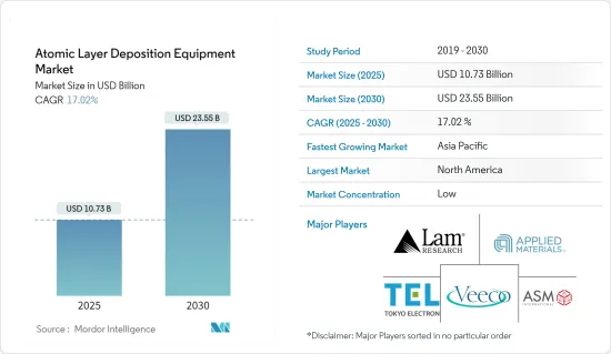
原子层沉积设备市场规模预计在 2025 年为 107.3 亿美元,预计到 2030 年将达到 235.5 亿美元,预测期内(2025-2030 年)的复合年增长率为 17.02%。
推动全球原子层沉积市场扩张的主要因素之一是全球电子和半导体解决方案的采用日益增加。
关键亮点
- 采用新材料和设计来提高晶片产量正在推动对原子层沉积解决方案的需求。小型化趋势正受到世界各地工业的青睐。因此,对小型电子设备和机器的需求日益增长。
- 据思科称,到 2030 年,约有 5,000 亿台设备将连接到网际网路。每台机器都包含收集资料、与环境互动并透过网路通讯的感测器。这些应用需要小型化的储存设备和积体电路。越来越多的连网设备产生的资料量也不断增加,增加了对储存设备的需求,从而推动了市场成长。
- 在半导体产业中,CMOS 处理器、储存设备、MEMS 和感测器中使用的高介电常数薄膜经常使用 ALD 技术生产。 ALD 技术用于在燃料电池和其他需要耐腐蚀和耐磨的应用中创建功能性和保护性涂层。在下一代设备的开发中,它们也被用于涂覆高长宽比结构,例如奈米线和奈米管。
- 随着众多创新和节能技术的发展,对轻便便携设备的需求正在迅速增长。原子层沉积技术在硅晶片的製造上有着广泛的应用。原子层沉积市场的成长预计将受到电子设备需求不断增长的推动。
- 此外,机器人和製造自动化的不断增加的使用预计将增加半导体销售并推动 ALD 技术市场的发展。工业自动化目前正在改变几乎所有重要製造业的性质。工业 4.0 标准的采用以及协作机器人、AR/VR 和 AI 在资料分析方面的日益使用预计将使 ALD 市场受益。
- 此外,ALD 薄膜层可用于微电子领域,对奈米级电晶体的相邻组件进行电屏蔽。 ALD 特别擅长将精确的奈米级涂层应用于复杂的3D表面。例如,它们类似于製造现代电脑处理器所使用的硅晶片上蚀刻的深而窄的凹槽。因此,世界各地的研究人员都渴望为未来几代半导体装置创造新的薄膜 ALD 材料。
- 预计预测期内,研发所需的高额投资将抑制全球原子层沉积市场的成长。由于该方法耗时,ALD 被认为是一个主要的限制因素。
原子层沉积设备的市场趋势
半导体和电子产业推动市场成长
- 预计半导体和电子产业的需求将成为原子层沉积技术的主要驱动力。预计半导体产业将对该技术的发展产生直接影响,而电子产业的扩张将促进该技术的发展。因此,对原子层沉积设备的需求正在上升
- 由于晶片短缺,製造商宣布扩大全球晶圆厂产能,原子层沉积 (ALD)参与企业正准备利用新的成长机会。最近,300 毫米 ALD 平台得到了改进,以满足超摩尔 (MtM) 设备、MEMS、感测器、电源和射频设备以及光电应用的要求。在此之前,200mm ALD 平台是为了满足市场需求而设计的。随着晶圆产量不断上升,ALD 解决方案预计将扩大并加入 MtM 设备市场。
- ALD 因沉积高介电常数氧化物材料而成为半导体产业的焦点。例如,我们以 ALD 形成的 HfO2 取代热生长的 SiO2 作为传统金属氧化物半导体场效电晶体中的闸极绝缘材料。近年来,需要使用 ALD 的应用数量显着增加。
- 电子行业存在週期性的起伏。电子业的短期至中期前景光明。爱立信的行动报告预测,到2024年,行动用户数将达到约89亿,行动宽频用户数将达到84亿,独立行动用户数将达到62亿。这有望加速 ALD 技术的发展。
- 预计预测期内家用电子电器和微电子产品销售的成长将推动半导体积体电路的需求。半导体积体电路需求的增加可能会提高半导体装置製造商的製造能力,从而增加对原子层沉积设备的需求。
- 下一代半导体装置的製造需要在低温(400°C)下在高长宽比比奈米结构上沉积高度保形(>95%)的SiO2、SiNx 和 SiC 薄膜。原子层沉积正日益取代半导体製造中的化学沉积方法,从而促进此类 Si 基电介质薄膜的开发。 ALD 沉积的 SiO2 薄膜已被用于半导体装置的製造。
- 射频和电力电子的扩展进一步推动了 ALD 技术的进步。恶劣的环境条件会损坏和腐蚀活性零件,导致过早失效。这些环境条件包括高温、氧气、紫外线、盐和湿气。原子层沉积 (ALD) 显着提高了这些组件的性能和可靠性。
亚太地区可望实现最高成长
- 亚太地区仍然是电子产业扩张的最重要地区。亚太地区是电子产业OEM的中心。此外,越南等新兴经济体正在大力投资该产业,从而导致不同地区的国家之间形成了良性竞争。此外,台湾和中国等成熟地区继续大力投资研发,使其在推动市场成长的技术创新方面保持领先一步。
- 原子层沉积通常用于太阳能电池和设备中的三防胶。在这方面,预计整个预测期内太阳能电池设备需求的不断增长以及各个地区太阳能电池行业的兴起将推动目标市场的发展。此外,亚太地区各国政府不断进行各种投资以扩大太阳能产业,这推动了对 ADL 解决方案的需求。
- 汽车是另一个在製造过程中使用 ALD 装置和系统的重要领域。汽车行业是薄膜的另一个主要用户,因为它们几乎应用于该行业的每个方面。例如,薄膜可以减小各种组件的尺寸并延长其使用寿命。在汽车领域,薄膜涂层可用于节省成本和保护环境。这是透过减轻常用结构元件的重量、提高其使用寿命以及提高奈米材料的製造品质来实现的。
- 亚洲是一些全球最大汽车製造商的所在地,包括本田、丰田、三菱、日产、现代、塔塔汽车和玛鲁蒂,而中国、印度、日本和韩国等国家则是亚洲汽车产业的强国。除了这些OEM之外,许多零件製造商和汽车配件製造商也使用 ALD 设备和机械来满足其製造需求。
- 半导体装置製造的一个重要方法是原子层沉积,这是一种依赖气相化学过程的薄膜沉积过程。该地区的参与企业正在大力投资研发项目,以提高产出效率并引领全球最快的市场扩张。
原子层沉积设备产业概况
原子层沉积设备市场呈现细分化,有多家参与企业在市场上运作。市场参与企业正在采取合併、收购和伙伴关係等策略来获得市场占有率。
- 2023 年 11 月 - 牛津仪器等离子技术赢得多家市场领先的日本代工厂的大量订单,用于製造 GaN HEMT 装置的等离子增强原子层沉积 (ALD) 和原子层蚀刻 (ALE)。该系统将支援高成长的GaN电力电子和高频市场,其中消费快速充电和资料中心应用处于电力电子市场的最前沿,5G/6G通讯应用处于高频市场。
- 2023 年 9 月 - Sky Water Technology 宣布将为客户提供用于原子层沉积 (ALD) 的新型半导体製程工具 Applied Picosun MorpherTM。许多设备(例如感测器和新储存技术)都需要能够在硅晶片上均匀沉积的薄层。
其他福利
- Excel 格式的市场预测 (ME) 表
- 3 个月的分析师支持
目录
第 1 章 简介
- 研究假设和市场定义
- 研究范围
第二章调查方法
第三章执行摘要
第四章 市场洞察
- 市场概况
- 产业吸引力-波特五力模型
- 供应商的议价能力
- 消费者议价能力
- 新进入者的威胁
- 替代品的威胁
- 竞争对手之间的竞争
- 产业价值链分析
- 技术简介:与其他沉积技术的比较、ALD 从记忆体到逻辑 MPU 应用的演变、ALD 技术类型的定性分析
- COVID-19 工业影响评估
第五章 市场动态
- 市场驱动因素
- 微电子和消费性电子产品的需求不断增长
- 运算和储存技术的进步
- 市场问题
- 高效的沉积试剂和材料,但会增加成本
第六章 市场细分
- 按应用
- 半导体和电子(包括计算领域、资料中心和消费性电子)
- 医疗和生物医学应用
- 车
- 其他的
- 按地区
- 美洲
- 欧洲、中东和非洲
- 亚洲
- 澳洲和纽西兰
第七章 竞争格局
- 公司简介
- Applied Materials Inc.
- Lam Research Corporation
- Entegris Inc.
- Veeco Instruments Inc.
- Oxford Instruments PLC
- Beneq Oy
- Picosun Oy
- ASM International
- Tokyo Electron Limited
- Kurt J. Lesker Company
第八章投资分析
第九章 市场机会与未来趋势
The Atomic Layer Deposition Equipment Market size is estimated at USD 10.73 billion in 2025, and is expected to reach USD 23.55 billion by 2030, at a CAGR of 17.02% during the forecast period (2025-2030).
One of the key factors propelling the expansion of the worldwide atomic layer deposition market is the increasing adoption of electronics and semiconductor solutions across the globe.
Key Highlights
- Using novel materials and designs for improved chip production drives demand for atomic layer deposition solutions. The trend toward miniaturization is being embraced by industries all around the world. As a result, there is currently a higher need for tiny electronics and machinery.
- According to Cisco, around 500 billion devices will be connected to the Internet by 2030. Each machine includes sensors that collect data, interact with the environment, and communicate over a network. These applications need miniaturized storage devices and ICs. The increasing amount of data generated from the growing number of connected devices has increased the demand for storage devices, thereby driving market growth.
- High-k dielectric films used in CMOS processors, memory devices, MEMS, and sensors are frequently produced using ALD in the semiconductor industry. For the creation of functional and protective coatings in fuel cells and other applications needing corrosion or wear resistance, ALD technologies are used. For the development of next-generation devices, they are also utilized to coat high aspect ratio structures like nanowires and nanotubes.
- Due to the development of a large number of innovation and energy efficient technologies, demand for lightweight portable devices has increased rapidly. For the production of silicon chips, atomic layer deposition technology is widely used. In the end, the growth of the atomic layer deposition market is expected to be driven by increasing demand for electronic devices.
- Additionally, it is anticipated that greater robot use and manufacturing automation will promote the market for ALD technology by increasing semiconductor sales. Industrial automation is currently transforming the nature of practically all significant production industries. The adoption of Industry 4.0 standards and the increasing use of collaborative robotics, AR/VR, and AI for data analysis are anticipated to benefit the ALD market.
- Moreover, the ALD thin layer may be utilized in microelectronics to shield neighboring components in nanoscale transistors electrically. ALD is particularly adept at creating accurate, nanoscale coatings on intricate, 3D surfaces; such as the deep, narrow trenches etched into silicon wafers used to make modern computer processors. This has inspired researchers worldwide to create novel thin film ALD materials for upcoming semiconductor device generations.
- Over the projected period, a high investment required for research and development is anticipated to restrain the growth of the worldwide atomic layer deposition market. ALD is recognized to have significant limitations due to its slow approach.
Atomic Layer Deposition Equipment Market Trends
Semiconductors and Electronics Industry to Drive the Market Growth
- The demand from the semiconductor and electronics industries is anticipated to be the primary driver of atomic layer deposition technology. While the semiconductor industry is expected to impact the technology's development directly, any electronics industry expansion will contribute to its advancement. Consequently, atomic layer deposition equipment is growing in demand.
- After the global fab capacity expansions that manufacturers announced as a result of the chip shortfall, Atomic Layer Deposition (ALD) players are prepared to take advantage of a new growth opportunity. Recently, 300mm ALD platforms have improved to satisfy the requirement of More-than-Moore (MtM) devices and applications for MEMS, sensors, power and RF devices, and photonics. Previously, 200mm ALD platforms were designed to fulfill the market's needs. Now that wafer production has increased in volume, it is anticipated that ALD solutions will expand and join the MtM devices market.
- ALD rose to prominence in the semiconductor industry due to its use for depositing high-permittivity oxide materials. For example, thermally grown SiO2 was swapped out for HfO2 formed by ALD as the gate dielectric material in conventional metal oxide semiconductor field effect transistors. The number of applications requiring the usage of ALD has significantly increased in recent years.
- The electronics sector has ups and downs in cycles. The short- to medium-term outlook for the electronic industry is positive. By 2024, there will be around 8.9 billion mobile subscriptions, 8.4 billion mobile broadband subscriptions, and 6.2 billion unique mobile users, predicts the Ericsson Mobility Report. This is anticipated to accelerate the development of ALD technology.
- During the projection period, growth in the sales of consumer electronics and microelectronics is anticipated to drive up demand for semiconductor ICs. The increased demand for semiconductor ICs will raise the manufacturing capabilities of semiconductor device producers, which might increase demand for the atomic layer deposition equipment market.
- Next-generation semiconductor device production necessitates the deposition of highly conformal (great than 95%) SiO2, SiNx, and SiC films on high aspect-ratio nanostructures at low temperatures (400 °C). Atomic layer deposition is replacing chemical vapor deposition in semiconductor manufacturing, allowing for the development of these Si-based dielectric films. ALD-deposited SiO2 films are already utilized in the production of semiconductor devices.
- The expansion of RF and power electronics further aids the advancement of ALD technology. Extreme environmental conditions can damage and corrode active components, leading to early failure. These conditions include high temperatures, oxygen, ultraviolet radiation, salinity, and moisture. The performance and dependability of these components can be significantly increased for the same reason, thanks to atomic layer deposition (ALD).
Asia Pacific Expected to Witness the Highest Growth Rate
- The Asia Pacific continues to be the most critical region for the proliferation of the electronics industry. The Asia Pacific has become a hub of OEMs in the electronics industry. Moreover, emerging economies like Vietnam have invested heavily in this industry, leading to healthy competition among various regional countries. Moreover, established hubs like Taiwan and China continue to invest heavily in R&D, enabling them to stay ahead of the curve in innovations that drive market growth.
- Atomic layer deposition is commonly utilized in solar cells and devices for conformal coatings. In light of this, the target market is anticipated to develop throughout the projected period due to the increase in demand for solar devices and the rise in the solar industry across various regional countries. Additionally, governments in the APAC region are constantly establishing various investments to increase their solar industry, which drives the demand for ADL solutions.
- The automobile is another significant sector that uses ALD units and Systems for its manufacturing. Automobile industries are another primary user of thin film, as it is used in practically every aspect of the industry. For example, the thin film can reduce the size and enhance the life of various parts. Thin coatings are used in the automotive sector to save money and the environment. This is done by reducing the weight of commonly used construction elements, enhancing their service life, and, as a result, improving the manufacturing quality of nanomaterials.
- Asia is the home of some of the biggest manufacturers of automobiles in the world, such as Honda, Toyota, Mitsubishi, Nissan, Hyundai, TATA Motors, Maruti, etc., with countries like China and India, Japan, and South Korea being the powerhouse of Asian Automobile Sector. Apart from these OEMs, many parts and automobile accessories suppliers also find usage for ALD units and equipment for their manufacturing requirements.
- A critical approach in producing semiconductor devices is atomic layer deposition, a thin-film deposition process that relies on the use of a gas-phase chemical process. The market's players in this region are heavily investing in research and development programs to improve their outcomes' efficiency and lead the fastest market expansion worldwide.
Atomic Layer Deposition Equipment Industry Overview
The Atomic Layer Deposition Equipment Market is fragmented, as several players are operating in the market. Players in the market adopt strategies like mergers, acquisitions, and partnerships to capture market share.
- November 2023 - Oxford Instruments Plasma Technology announces significant order placements for plasma atomic layer deposition (ALD) and atomic layer etch (ALE) for GaN HEMT device production from several market-leading Japanese foundries. The systems will support high-growth GaN power electronics and radio frequency markets, with consumer fast-charging and datacentre applications at the forefront for power electronics, and 5G/6G communication applications for the radio frequency market.
- September 2023 - Sky water technology announced it will provide customers a new semiconductor processing tool for Applied Picosun MorpherTM, atomic layer deposition (ALD) . The thin layers that can be deposited uniformly across the entire silicon wafer are required by a number of devices, such as sensors and emerging memory technology.
Additional Benefits:
- The market estimate (ME) sheet in Excel format
- 3 months of analyst support
TABLE OF CONTENTS
1 INTRODUCTION
- 1.1 Study Assumptions and Market Definition
- 1.2 Scope of the Study
2 RESEARCH METHODOLOGY
3 EXECUTIVE SUMMARY
4 MARKET INSIGHTS
- 4.1 Market Overview
- 4.2 Industry Attractiveness - Porter Five Forces
- 4.2.1 Bargaining Power of Suppliers
- 4.2.2 Bargaining Power of Consumers
- 4.2.3 Threat of New Entrants
- 4.2.4 Threat of Substitute
- 4.2.5 Intensity of Competitive Rivalry
- 4.3 Industry Value Chain Analysis
- 4.4 Technology Snapshot : Comparison with other deposition technologies and evolution of ALD from Applications in Memory to Application in Logic MPUs and Qualitative analysis regarding type of ALD technologies
- 4.5 Assessment of COVID-19 Impact on the Industry
5 MARKET DYNAMICS
- 5.1 Market Drivers
- 5.1.1 Increase in demand of Microelectronics and Consumer Electronics
- 5.1.2 Advancement in Computing and Storage Technologies
- 5.2 Market Challenegs
- 5.2.1 Higher Associated costs due to Effective Deposition Reactants and Materials
6 MARKET SEGMENTATION
- 6.1 By Application
- 6.1.1 Semiconductor and Electronics (includes Computing Sector, Data Centres, and Consumer Electronics)
- 6.1.2 Healthcare and Biomedical Applications
- 6.1.3 Automotive
- 6.1.4 Other Applications
- 6.2 By Geography
- 6.2.1 Americas
- 6.2.2 Europe, Middle East and Africa
- 6.2.3 Asia
- 6.2.4 Australia and New Zealand
7 COMPETITIVE LANDSCAPE
- 7.1 Company Profiles
- 7.1.1 Applied Materials Inc.
- 7.1.2 Lam Research Corporation
- 7.1.3 Entegris Inc.
- 7.1.4 Veeco Instruments Inc.
- 7.1.5 Oxford Instruments PLC
- 7.1.6 Beneq Oy
- 7.1.7 Picosun Oy
- 7.1.8 ASM International
- 7.1.9 Tokyo Electron Limited
- 7.1.10 Kurt J. Lesker Company
8 INVESTMENT ANALYSIS
9 MARKET OPPORTUNITIES AND FUTURE TRENDS
 原子层沉淀设备市场(按设备类型、技术类型、应用和最终用户产业划分)-2025-2032年全球预测原子层沉积市场(按设备类型、材料、应用和最终用户产业)—全球预测 2025-2032
 2025年原子层沉淀全球市场报告2025年全球ALD设备市场报告
 原子层沉积 (ALD) 市场 - 全球产业规模、份额、趋势、机会和预测(按类型、按材料、按最终用途行业、按地区和竞争细分,2020-2030 年)
 全球半导体 ALD 和 CVD 前驱市场
 原子层沉积 (ALD) 市场预测(至 2032 年):按产品类型、应用、最终用户和地区进行的全球分析
 全球 ALD 设备市场研究报告 - 产业分析、规模、份额、成长、趋势及 2025 年至 2033 年预测
 原子层沉积设备市场报告(按产品(金属 ALD、氧化铝 ALD、等离子体增强 ALD、催化 ALD 等)、应用(半导体、太阳能设备、电子产品、医疗设备等)和地区)2025 年至 2033 年全球原子层沉积市场研究报告-产业分析、规模、份额、成长、趋势与预测 2025 年至 2033 年