


 |
市场调查报告书
商品编码
1406267
半导体光刻设备:市场占有率分析、产业趋势与统计、2024年至2029年成长预测Semiconductor Lithography Equipment - Market Share Analysis, Industry Trends & Statistics, Growth Forecasts 2024 - 2029 |
||||||
※ 本网页内容可能与最新版本有所差异。详细情况请与我们联繫。
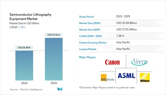
预计2024年半导体光刻设备市场规模为264.8亿美元,2029年预计将达378.1亿美元,在预测期内(2024-2029年)复合年增长率为7.38%。
主要亮点
- 由于广泛应用于消费性电子和汽车等几乎所有领域的半导体装置製造规模的扩大,全球半导体光刻设备市场预计将成长。智慧型设备的采用正在不断增加,并且预计随着 5G 连接和采用在全球范围内的普及,智慧型设备的采用也会不断增长。根据GSMA预测,2025年5G行动宽频连线预计将达到11亿,到2025年5G普及预计将覆盖全球34%的人口。
- 超过50%的半导体FAB(製造)成本来自于设备和工具。光刻是推进半导体製造製程的设备之一。半导体製造的多个方面都依赖光刻设备。从技术角度来看,产量比率和缺陷就是两个这样的例子。这是半导体製造如此关注采用哪种类型的光刻技术的主要原因。
- 随着半导体产品变得越来越复杂,缺陷的类型也越来越复杂。然而,光刻设备被设计用来处理这个复杂的过程。随着半导体製造商专注于下一代先进技术节点,无错误光刻设备变得更加重要。
- 此外,随着 5G 和物联网连接设备的出现,製造业最近经历了显着增长,预计将促进无线控制等各种工业 4.0 应用所需的连接。这对于移动工具、机械和机器人尤其重要,可以帮助预测期内的市场成长。
- 多家产业公司致力于为各种应用提供新型光刻系统。例如,尼康公司将于2022年3月推出全新第8代平板FPD光刻系统,该系统将支援高阶显示器、大型电视和智慧型手机等高付加优质显示器的各种高清面板的生产。设备. 宣布.
- 半导体产业是最复杂的产业之一,拥有 500 多个製造和测试流程。因此,根据製造流程的复杂程度,半导体晶圆的完整製造和检验大约涉及1,400个步骤。这一复杂的过程对市场成长构成了显着的障碍。
- 相反,在对下一代电子产品的强劲需求的支持下,COVID-19 大流行使资本设备产业持续成长。 SEMI 的数据显示,2021 年全球半导体製造设备销售额激增 44%,达到 1,026 亿美元,高于去年同期的 712 亿美元。
半导体光刻设备市场趋势
深紫外光刻(DUV)占据主要市场占有率
- 深紫外光刻 (DUV) 是一种光学投影微影技术,其中光罩上的图案透过 4 倍或 5 倍光学元件投影到晶圆表面。这种类型的光刻所使用的波长是248nm或193nm。这种微影技术是一种高速微影技术,非常适合对 22mm x 22mm 以下的分立元件进行大面积母版处理,22mm x 22mm 是 DUV 工具的典型晶圆级曝光场尺寸。
- DUV光刻类型是具有代表性的下一代光刻技术之一。该技术具有成本效益,并提供更高的解析度。 DUV 微影技术的采用主要是由小型化趋势所推动的。光刻用于在半导体晶圆上印刷表征积体电路 (IC) 的复杂图案。
- DUV 微影可以轻鬆创建低功耗的轻量电子晶片。该平台提供了改进的功率分辨率并且具有成本效益。这些结构一起形成一个 IC,称为晶片。半导体产业对更高效微晶片的追求意味着晶片製造商需要研究晶片上的更多结构,使其速度更快、效率更高,同时降低製造成本。预计这将推动预测期内的市场成长。
- ASML 表示,向 EUV 的过渡可能会进一步增加对 DUV 的需求。晶片製造商在晶片製造的早期阶段引入EUV,应用电晶体、最小通孔(将源极、闸极和汲极连接到复杂互连层的接点)等微结构,以及在某些情况下的连接层。
- 随着公司寻求能够製造高达 7 奈米节点晶片的技术,市场正在见证各种投资。例如,Canon于2022年10月宣布将在日本东部建立新的半导体设备工厂,生产半导体光刻设备等产品。该设施预计将于 2025 年上半年运作。
- 领先供应商的此类市场开拓以及政府提高半导体产量的倡议预计将在预测期内推动市场成长。
美国占有很大份额
- 美国拥有强大的半导体研发能力,大量投资扩大半导体製造能力,快速引进尖端技术。
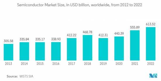
- 此外,美国对半导体的需求正在增加。例如,根据2021年9月世界半导体贸易统计数据(WSTS),2021年半导体产业销售额大幅成长至5,270亿美元,主要得益于2020年整个市场需求成长强劲。该预测已上修。 WSTS 预测 2022 年全球销售额将达到 5,730 亿美元。
- 此外,根据半导体设备与材料国际公司的数据,2022 年 4 月,北美半导体设备支出在 2021 年达到 76.1 亿美元,而 2020 年为 65.3 亿美元。
- 半导体产业团体也表示,美国半导体产业在晶片设计方面处于领先地位。美国无厂半导体公司约占全球无厂半导体公司销售额的60%,安排无晶圆厂销售额的一些最大的IDM都是美国公司。
- 根据美国半导体产业的状况,2019年运行在半导体晶片上的连网型设备(ioT:物联网)价值达到226亿美元,预计到2025年将达到750亿美元。半导体也是 3D 列印、机器学习和人工智慧 (AI) 等创新的基础,这些创新可改善医疗保健、降低建筑成本、增强食品供应并促进科学进步。该地区对半导体的强劲需求可能会推动预测期内半导体光刻设备的采用。
- 此外,2022年9月,拜登政府宣布美国将发展国内半导体产业,以对抗对中国的依赖,因为美国零产量,只消费量了全球最先进晶片的25%,而这些晶片对于美国来说至关重要。为了国家安全,宣布将投资500亿美元拜登总统于 2022 年 8 月签署了 2800 亿美元的 CHIPS 法案,以促进国内高科技製造业,作为增强美国对中国竞争力的努力的一部分。该地区半导体行业如此强劲的投资可能会为研究市场的成长提供利润丰厚的机会。
半导体光刻设备产业概况
该市场集中在 ASML、Veeco 和 Nikon 等少数供应商手中。半导体製造的主要设备基本上被美国和日本企业垄断。由于整合不断增加、技术进步和地缘政治形势,所研究的市场正在经历波动。此外,随着垂直整合的推进,考虑到投资与收益的匹配能力,市场竞争预计将继续加剧。
- 2022年9月-Canon发布半导体光刻设备解决方案平台「Lithography Plus1」。我们将Canon50多年的半导体光刻设备支援经验和大量资料融入我们的系统中,以最大限度地提高支援效率,并提案并实现最佳的系统流程。
- 2022 年 6 月 - 三星和 ASML 同意合作开发 High-NA(高数值孔径)EUV 光刻设备,并于明年开始销售。与传统 EUV 微影设备相比,新一代高数值孔径 EUV 微影设备可以形成更小的电路。
其他福利:
- Excel 格式的市场预测 (ME) 表
- 3 个月分析师支持
目录
第一章简介
- 研究假设和市场定义
- 调查范围
第二章调查方法
第三章执行摘要
第四章市场洞察
- 市场概况
- 产业吸引力-波特五力分析
- 供应商的议价能力
- 买方议价能力
- 新进入者的威胁
- 替代品的威胁
- 竞争公司之间的敌对关係
- 半导体光刻设备技术蓝图
- 宏观经济走势对市场的影响
第五章市场动态
- 市场驱动因素
- 由于电动车和先进的移动设备,对更小尺寸和更高功能的需求不断增加
- 专业设备供应商提供新型光刻设备,技术创新进步
- 市场抑制因素
- 製造过程中与图案复杂性相关的挑战
第六章市场区隔
- 类型
- 深紫外光微影 (DUV)
- 极紫外光刻(EUV)
- 目的
- 先进封装
- 微机电系统元件
- LED元件
- 地区
- 北美洲
- 欧洲
- 亚太地区
- 世界其他地区
第七章 竞争形势
- 公司简介
- Canon Inc.
- Nikon Corporation
- ASML Holding NV
- Veeco Instruments Inc.
- SUSS MicroTec SE
- Shanghai Micro Electronics Equipment(Group)Co. Ltd
- EV Group(EVG)
- JEOL Ltd
- Onto Innovation(Rudolph Technologies Inc.)
- Neutronix Quintel Inc.(NXQ)
- 供应商市场占有率分析
第八章投资分析
第9章市场的未来
The Semiconductor Lithography Equipment Market size is estimated at USD 26.48 billion in 2024, and is expected to reach USD 37.81 billion by 2029, growing at a CAGR of 7.38% during the forecast period (2024-2029).
Key Highlights
- The global semiconductor lithography equipment market is expected to grow with the growing manufacturing of semiconductor devices that are widely used in nearly all sectors including consumer electronics, automotive, and many others. Smart device adoption is increasing and is expected to grow as 5G connections and adoption spread over the globe. As per GSMA, 5G mobile broadband connections are expected to reach 1,100 million by 2025, with the 5G rollout expected to cover 34 percent of the world's population by 2025.
- More than 50 percent of the semiconductor FAB (fabrication) cost is due to equipment and tools. One piece of equipment that drives the semiconductor fabrication process forward is lithography. There are several aspects of semiconductor fabrication that has driven by lithography equipment. Yield and defect are two such examples from the technical point of view. It is the primary reason why semiconductor fabrication focuses a lot on which type of lithography technology to deploy.
- With the rising complexity in semiconductor products, the types of defects are also getting complex. However, lithography equipment is supposed to handle the complex process. With semiconductor manufacturers focusing on next-gen advanced technology nodes, the importance of error-free lithography equipment is significantly increasing further.
- Moreover, manufacturing businesses are are lately growing at a signficant rate with the advent of 5G and emergence of IoT connected devices, which is anticipated to facilitate the connection required for various Industry 4.0 applications, such as wireless control. This is especially essential for mobile tools, machines, and robots that can aid market growth during the forecast period.
- Several industry players are focusing on offering new lithography systems to serve a wide range of applications. For instance, in March 2022, Nikon Corporation announced to launch new Gen 8 plate FPD lithography system to support the production of various high-definition panels for value-added premium displays, such as high-end monitors, large TVs, and smart devices.
- The semiconductor industry is considered as one of the most complex industries, not only owing to the presence of more than 500 processing steps involved in the manufacturing and inspection and various products but also due to the harsh environment it goes through, e.g., the volatile electronic market and the unpredictable demand. Therefore, depending on the intricacy of the manufacturing process, there are about 1,400 process steps in the complete manufacturing and inspection of semiconductor wafers alone. Such a complex process poses a notable hurdle to the market's growth.
- On the contrary, the COVID-19 pandemic kept the capital equipment sector growing with a strong demand for next-generation electronics. As per SEMI, the global sales of semiconductor manufacturing equipment surged by 44 percent in 2021 to a record of USD 102.6 billion, up from USD 71.2 billion in the previous year.
Semiconductor Lithography Equipment Market Trends
Deep Ultraviolet Lithography (DUV) to Hold Major Market Share
- Deep UV lithography (DUV) is an optical projection lithography technique where the pattern on the mask is projected to the wafer surface through a 4X or 5X optical system. The wavelengths used for this type of lithography are 248 nm or 193 nm. This lithography is a high-speed lithographic technology ideal for large-area masters of discrete components that are not bigger than 22 mm x 22 mm, the typical wafer-level exposure field size of a DUV tool.
- The DUV lithography type is one of the leading lithography technologies of the next generation. The technology is cost-effective and has increased resolving power. The adoption of DUV lithography is driven primarily by the miniaturization trend. Lithography is used for printing complex patterns that characterize integrated circuits (ICs) on semiconductor wafers.
- Using DUV lithography, lightweight electronic chips with lower power demands are easy to achieve. The platform features enhanced power resolution and is cost-effective. These structures together form an IC, which is known as a chip. The semiconductor industry's search for even more efficient microchips means chipmakers have to study more structures onto a chip, making the chip faster and more efficient while also reducing production costs. This is expected to boost the market's growth over the forecast period.
- According to ASML, a transition to EUV may only boost demand for DUV. Chip manufacturers deploy EUV in the early stages of chip fabrication to apply the minor structures: transistors, smallest vias (the contacts that connect the source, gate, and drain to the complex interconnect layers), and possibly the connecting layer.
- The market is witnessing various investments as the companies are seeking a technology that can produce chips down to 7nm nodes. For instance, in Oct 2022, Canon announced the development of a new semiconductor equipment plant in eastern Japan which will produce semiconductor lithography systems and other devices. The facilities are expected to commence operation by the first half of 2025.
- Such developments by the major vendors, along with the initiatives taken by the government to boost their semiconductor production, are expected to drive market growth over the forecast period.
United States to Witness Significant Share
- The United States boasts robust semiconductor R&D capabilities, significant investments catering to the expansion of semiconductor manufacturing capabilities, and rapid adoption of advanced technologies.
- Further, the United States is witnessing an increasing demand for semiconductors. For instance, in September 2021, according to the world semiconductor trade statistics (WSTS), semiconductor industry sales increased significantly to USD 527 billion in 2021, an upward revision from the 2020 forecast for 2021 due mainly to the strong demand growth in the overall market 2020. In 2022, WSTS forecasted global sales totaled to USD 573 billion.
- Additionally, in April 2022, according to Semiconductor Equipment and Materials International, North America's spending on semiconductor equipment reached USD 7.61 billion in 2021 compared to 2020, which was USD 6.53 billion.
- Also, the semiconductor industry association stated that the US semiconductor industry is a leader in chip design. The United States fabless firms account for roughly 60 percent of all global fabless firm sales, and some of the largest IDMs, which make their arrangement, are also US firms.
- According to the state of the US semiconductors industry, the connected devices that run on semiconductor chips (i.e., the Internet of Things (IoT)) registered USD 22.6 billion in 2019 and are expected to reach USD 75 billion by 2025. Semiconductors are also fundamental to innovations, such as 3D printing, machine learning, and artificial intelligence (AI) that enhance healthcare, reduce building costs, strengthen food supply, and enable advancements in science. The region's robust semiconductor demand is likely to boost the adoption of semiconductor lithography equipment during the forecast period.
- Additionally, in September 2022, the Biden administration announced that it would invest USD 50 billion in building up the domestic semiconductor industry to counter dependency on China, as the US produces zero and consumes 25 percent of the world's leading-edge chips vital for its national security. President Joe Biden signed a USD 280 billion CHIPS bill in August 2022 to boost domestic high-tech manufacturing, part of his administration's push to boost US competitiveness over China. Such robust investments in the semiconductor sector in the region would offer lucrative opportunities for the growth of the studied market.
Semiconductor Lithography Equipment Industry Overview
The market is concentrated due to a few vendors such as ASML, Veeco, and Nikon occupying the majority market share. The key equipment for semiconductor manufacturing is basically monopolized by American and Japanese companies. With growing consolidation and technological advancement, and geopolitical scenarios, the studied market is witnessing fluctuation. In addition, with increasing vertical integration, the intensity of competition in the studied market is expected to continue to rise, considering their ability to invest, which results from their revenues.
- September 2022 - Canon Inc. launched the "Lithography Plus1" solution platform for semiconductor lithography systems. Canon's more than 50 years of experience in semiconductor lithography system support and the company's vast wealth of data are incorporated into the system to maximize support efficiency and propose and implement optimized system processes.
- June 2022 - Samsung and ASML have agreed to collaborate on developing High-NA (high numerical aperture) EUV Lithography equipment, which will be available next year. Compared to older EUV Lithography equipment, the next-generation High-NA EUV Lithography equipment can engrave finer circuits.
Additional Benefits:
- The market estimate (ME) sheet in Excel format
- 3 months of analyst support
TABLE OF CONTENTS
1 INTRODUCTION
- 1.1 Study Assumptions and Market Definition
- 1.2 Scope of the Study
2 RESEARCH METHODOLOGY
3 EXECUTIVE SUMMARY
4 MARKET INSIGHTS
- 4.1 Market Overview
- 4.2 Industry Attractiveness - Porter's Five Forces Analysis
- 4.2.1 Bargaining Power of Suppliers
- 4.2.2 Bargaining Power of Buyers
- 4.2.3 Threat of New Entrants
- 4.2.4 Threat of Substitute Products
- 4.2.5 Intensity of Competitive Rivalry
- 4.3 Semiconductor Lithography Equipment Technology Roadmap
- 4.4 The impact of macroeconomic trends on the Market
5 MARKET DYNAMICS
- 5.1 Market Drivers
- 5.1.1 Increasing Demand for Miniaturization and Extra Functionality by Electric Vehicles and Advanced Mobile Devices
- 5.1.2 Growing Innovation by Specialist Equipment Vendors offering Brand New Lithography Tools
- 5.2 Market Restraints
- 5.2.1 Challenges Regarding Complexity of Pattern in Manufacturing Process
6 MARKET SEGMENTATION
- 6.1 Type
- 6.1.1 Deep Ultraviolet Lithography (DUV)
- 6.1.2 Extreme Ultraviolet Lithography (EUV)
- 6.2 Application
- 6.2.1 Advanced Packaging
- 6.2.2 MEMS Devices
- 6.2.3 LED Devices
- 6.3 Geography
- 6.3.1 North America
- 6.3.2 Europe
- 6.3.3 Asia Pacific
- 6.3.4 Rest of the World
7 COMPETITIVE LANDSCAPE
- 7.1 Company Profiles*
- 7.1.1 Canon Inc.
- 7.1.2 Nikon Corporation
- 7.1.3 ASML Holding NV
- 7.1.4 Veeco Instruments Inc.
- 7.1.5 SUSS MicroTec SE
- 7.1.6 Shanghai Micro Electronics Equipment (Group) Co. Ltd
- 7.1.7 EV Group (EVG)
- 7.1.8 JEOL Ltd
- 7.1.9 Onto Innovation (Rudolph Technologies Inc.)
- 7.1.10 Neutronix Quintel Inc. (NXQ)
- 7.2 Vendor Market Share Analysis


