


 |
市场调查报告书
商品编码
1692440
半导体前端设备:市场占有率分析、产业趋势与统计、成长预测(2025-2030 年)Semiconductor Front End Equipment - Market Share Analysis, Industry Trends & Statistics, Growth Forecasts (2025 - 2030) |
||||||
※ 本网页内容可能与最新版本有所差异。详细情况请与我们联繫。
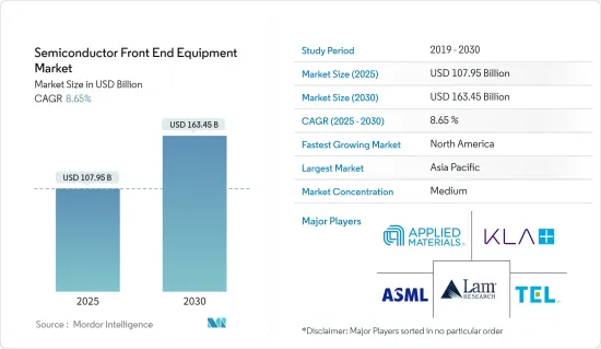
预计 2025 年半导体前端设备市场规模为 1,079.5 亿美元,到 2030 年将达到 1,634.5 亿美元,预测期内(2025-2030 年)的复合年增长率为 8.65%。
前端处理涉及许多复杂的步骤,以将晶圆转化为成品设备。这些阶段包括晶圆清洗、氧化、光刻以对装置进行图案化、蚀刻、沉淀、掺杂、金属化和其他步骤。检查和测量设备用于製程控制。这涉及检查晶圆以识别可能导致最终产品出现问题的不规则之处。除此之外,还使用光学技术,通常需要电子束检查才能发现即使是最小的缺陷。
主要亮点
- 在半导体产业低迷的背景下,主要前端设备製造商实现了创纪录的收益,预计半导体前端设备设备的需求将大幅成长,而不是经历短期调整。这是由产能扩张、新晶圆厂计划以及前端设备市场对先进技术和解决方案的高需求所推动的。
- 这一萎缩较去年晶圆製造设备(包括晶圆加工设备、晶圆厂设施以及掩模版和光罩设备)的销售额大幅增长相比有了显着改善,目前预测这些设备到 2023 年的销售额将略有下降。上调主要原因是中国有利的资本投资。在应对地缘政治挑战(包括美国和荷兰政府的出口管制限制)带来的不确定性以及对通膨、利率上升和某些经济体 GDP 成长放缓的全球宏观担忧的同时,市场也在成长。
- 家用电子电器是成长最快的领域,促进了市场扩张。智慧型手机的使用量预计会随着人口的成长而增加,这是该市场的主要驱动力。由于对平板电脑、智慧型手机、笔记型电脑、个人电脑、穿戴式装置等的需求不断增长,消费性电子产品正在推动产业发展。随着半导体的发展,机器学习等新的细分市场正在迅速整合。
- 未来最令人兴奋的「必赢」技术,包括人工智慧、物联网、量子运算和增强型无线网络,目前都是由半导体驱动的。随着世界将突破性技术无缝融入生活的各个方面,半导体和微电子技术正在不断发展以满足不断变化的数位环境的复杂需求。巨量资料和人工智慧正在推动这一成长,要求更小、更强大、更难製造的晶片,并推动创新的需求。
- 资料储存、运算能力和演算法的快速进步使得开发和部署人工智慧系统成为可能。数位设备和互联网的使用日益增加导致了大量数据的产生。人工智慧系统依靠大型资料集来学习和改进。
- 工业4.0的概念包含物联网(IoT)、巨量资料、云端製造、资讯物理系统(CPS)、服务互联网(IoS)、机器人、扩增实境(AR)等新兴技术。这些技术的采用对于创建更智慧的工业流程至关重要,这将涵盖一些将物理世界和数位世界结合在一起的未来工业进步。
- 随着全球在家工作趋势的增强,对云端服务的需求将激增,迫使资料中心供应商扩大其容量。这将导致全球对晶片和记忆体的需求增加。 SEMI报告称,对300毫米晶圆厂的投资正在大幅增加。预测显示,2020 年至 2024 年间,该产业将新增至少 38 座 300 毫米晶圆厂。
- 此次增产将使晶圆产能增加约180万片,使总合达到700万片以上。值得注意的是,台湾计划建造 11 座新的量产工厂,其次是中国大陆,计划建造 8 座。此外,台积电正在亚利桑那州建造一座新的 300 毫米晶圆厂。 2024年底,300mm量产工厂数量预计将达到161家。
半导体前端设备市场趋势
半导体製造工厂成为最大的终端用户产业
- 设计阶段结束后,半导体晶片在称为晶圆厂或铸造厂的设施中製造。在前端製造中,晶片是在称为晶圆的圆形硅片上製造的,或者不太常见的是在其他半导体材料上製造的。
- 製造是将设计转化为晶片的过程,依赖各种中小型公司和材料。首先,在熔炉中形成硅圆柱体,然后将其切割成圆盘状晶片。半导体製造厂(「晶圆厂」)透过两个步骤将晶片变成晶圆:在硅材料层中形成电晶体和其他电子装置,然后在硅顶部的绝缘层中形成电子元件之间的金属互连。电气设备和互连元件组合起来形成电路。
- 总部位于美国、台湾、韩国、日本和中国的公司控制着全球大部分半导体代工市场占有率和製造产能,而这些公司的实际所在地也位于这些国家。开发半导体产品需要许多企业(从材料到物流)的协同合作。半导体装置的製造流程复杂,增加了开发成本。企业纷纷采用各种经营模式来降低开支,并依赖半导体生存。
- 2023年11月,中国引进了42台微影术系统,价值8.168亿美元。荷兰提供了16台微影术系统,总价值7.627亿美元,比前一年增长了10倍。此外,中国10月从荷兰进口了21套系统。日本Canon、尼康也向中国供应曝光设备。因此,预计半导体製造厂前端设备的需求将会上调。
- 随着全球经济有望復苏,由于明年智慧型手机、伺服器、笔记型电脑、电视和汽车市场的成长,以及包括 5G基地台和 Wi-Fi 6 技术在内的下一代网路的持续推出,预计对零件的需求将增加。
- 根据欧洲5G观察站的数据,截至2023年,德国将成为欧盟成员国中5G基地台数量最多的国家,安装的基地台数量约为9万个。这些晶片的设计和製造以及背后的研究可以提供数十万个高薪工作岗位,使在岸/迴岸成为一个热门的政治话题。因此,铸造厂和设备製造商正在自己的后院规划和规划巨额投资。例如,东京电子已宣布计划在日本的设备製造工厂投资超过6亿美元。
- IDM 透过投资晶圆製造能力继续发挥关键作用。例如,2023年6月,英特尔与德国政府宣布签署修订后的意向书,计画在马德堡建立一个投资超过300亿欧元的尖端晶圆製造地,打造欧洲首批两座半导体工厂。根据韩媒报道,该公司计划于2023年12月从ASML收购六台高NA EUV曝光机台,并于2024年出货,此次收购被视为该公司在2nm节点超越三星、台积电的秘密武器。
- 2023年7月,三星宣布将投资170亿美元在德克萨斯州奥斯汀建造一座占地1,200英亩的半导体製造厂。中国和台湾之间的地缘政治紧张局势导致晶片製造商寻求在美国製造地。凭藉低税收和新的补贴,德克萨斯已成为开展业务的好地方。全球半导体製造设备製造商正在扩建其在韩国的工厂。中国政府计划在未来 20 年内投资 2,300 亿美元建造新的国内製造基地,以吸引其他公司并培育晶片供应链。
中国可望占主要市场占有率
- 据CSET称,除组装和包装工具外,中国在所有主要领域都占有相当大的市场占有率。但在微影术设备方面,特别是极紫外线(EUV)微影术和深紫外线(DUV)微影术,中国面临的挑战最大。
- 压印微影术、电子束、雷射微影术、抗蚀剂处理设备、光掩模检查和修復工具是主要障碍。过去几年,中国持续投入进口先进的微影术设备,以支持其晶片产业的发展。
- 然而,凭藉着强大的技术力,中国不断加大对前端设备的依赖,并进行大规模投资将其推向市场。
- 2023年12月,中国微影术设备专家上海微电子设备集团有限公司(SMEE)推出了第一台能够使用尖端28奈米级製程技术处理晶圆的机器。这项重大成就凸显了SMEE致力于打造先进微影术工具的决心。这款名为 SSA/800-10W 的设备标誌着该公司的一个重要里程碑。
- 在日本和中国之间的技术僵局不断升级的情况下,美国的製裁旨在阻碍中国在开发世界上最先进晶片方面的进展。中芯国际等晶片製造商致力于透过推进晶片生产来增强国家自主权。中芯国际正在利用先进的微影术设备,与本地设备製造商密切合作,并寻求华为的外部援助,以提高先进节点製程的产量比率。
- 由于美国持续对中国技术实施制裁,该地区正在努力自给自足。中国政府正大力投资先进晶片技术的研发。它还鼓励本地製造商将重点转向在经济和电动车(EV)等新兴产业中具有多种应用的更高节点晶片。政府的倡议不断增多以及本地供应商为提高国内晶片产量而增加的投资预计将在前端市场创造显着的需求。
- 根据中汽协统计,2023年8月中国新能源车销量约84.6万辆,其中搭乘用80.8万辆,商用车3.9万辆。其中,纯电动车(BEV)搭乘用保有量为55.9万辆,插电式混合动力电动车(PHEV)搭乘用保有量为24.8万辆。
半导体前端设备市场概况
半导体前端设备市场由应用材料公司主导。市场参与者正在采用伙伴关係、创新和收购等策略来加强其产品供应并获得可持续的竞争优势。
- 2024 年 2 月-ASML Holding NV 推出最新的晶片製造机 High-NA,其重量相当于两架空中巴士 A320 飞机,耗资 3.5 亿欧元。英特尔已确保其奥勒冈工厂的首批货物,预计明年年底开始生产晶片。该机器将实现厚度为8奈米的半导体线路,比传统型号小1.7倍,并提高晶片的晶体管密度,从而提高处理速度和记忆体。
- 2024 年 1 月-应用材料公司与Google合作推进扩增实境(AR) 技术。此次合作将利用应用材料公司的材料工程专业知识和Google的平台,为下一代 AR 体验开发轻量级视觉显示系统。目标是加速多代 AR 产品、应用和服务的开发。
其他福利
- Excel 格式的市场预测 (ME) 表
- 3个月的分析师支持
目录
第一章 引言
- 研究假设和市场定义
- 研究范围
第二章调查方法
第三章执行摘要
第四章 市场洞察
- 市场概览
- 产业吸引力-波特五力分析
- 供应商的议价能力
- 买家的议价能力
- 新进入者的威胁
- 替代品的威胁
- 竞争程度
- 产业价值链分析
- COVID-19 疫情对市场的影响
第五章市场动态
- 市场驱动因素
- 家用电子电器需求不断成长推动製造业前景
- 人工智慧、物联网和连网型设备在各行业的普及情况
- 市场限制
- 此技术的动态特性使得製造设备必须进行多项变革
第六章市场区隔
- 按类型
- 光刻设备
- 蚀刻设备
- 沉淀设备
- 其他设备类型
- 按最终用户产业
- 半导体製造厂
- 半导体电子製造
- 按地区
- 美国
- 欧洲
- 中国
- 韩国
- 台湾
- 日本
- 拉丁美洲
- 中东和非洲
第七章竞争格局
- 公司简介
- Applied Materials Inc.
- ASML Holding NV
- Tokyo Electron Limited
- LAM Research Corporation
- KLA Corporation
- Nikon Corporation
- VEECO Instruments Inc.
- Plasma Therm
- Hitachi High-Technologies Corporation
- Carl Zeiss AG
- Screen Holdings Co. Ltd
第八章投资分析
第九章:市场的未来
The Semiconductor Front End Equipment Market size is estimated at USD 107.95 billion in 2025, and is expected to reach USD 163.45 billion by 2030, at a CAGR of 8.65% during the forecast period (2025-2030).
The front-end procedure necessitates a multitude of intricate phases to convert a wafer into a completed device. These steps incorporate wafer cleaning, oxidation, and photolithography to pattern devices, along with etching, deposition, doping, and metallization steps. Inspection and metrology equipment is utilized for process control. This is when the wafers are inspected to identify irregularities that potentially induce issues with the end product. In addition to this, optical techniques are also used, and e-beam inspection is often needed to find the smallest defects.
Key Highlights
- The demand for semiconductor front-end equipment is expected to observe a noteworthy surge as some of the major front-end equipment-producing companies observed record-breaking revenue against a backdrop of a downturn in the semiconductor industry instead of the mild and short-term correction. It was driven by capacity expansion, new fab projects, and high demand for advanced technologies and solutions across the front-end equipment market.
- After registering a record of significant sales last year, the wafer fab equipment, which includes wafer processing, fab facilities, and mask/reticle equipment, is projected to be a bit low in 2023, and this contraction marks a significant improvement. The upward revision is primarily due to China's strong equipment spending. The market grew managing uncertainties created by geopolitical challenges, including the US and Dutch governments' export control regulations and global macro concerns around inflation, rising interest rates, and lower GDP growth in certain economies.
- Consumer electronics is the fastest-growing segment, contributing to market expansion. The use of smartphones, anticipated to rise with population growth, is the key driver of this market. Consumer electronics drive the industry due to increased demand for tablets, smartphones, laptops, computers, and wearable gadgets. As semiconductors advance, new market areas, such as machine learning, are rapidly being integrated.
- The most fascinating "must-win" technologies of the future, such as artificial intelligence, the Internet of Things, quantum computing, and enhanced wireless networks, are currently supported by semiconductors. Semiconductors and microelectronics are advancing to satisfy the complicated demands of a constantly changing digital environment as the world seamlessly integrates breakthrough technology into every aspect of life. Big Data and AI drive this increase and call for smaller, more powerful chips, making their production more difficult and increasing the need for technological innovation.
- Rapid advancements in data storage, computing power, and algorithms have enabled the development and deployment of AI systems. The increased use of digital devices and the Internet has generated extensive volumes of data. AI systems rely on large datasets to train and improve their performance.
- The Internet of Things (IoT), big data, cloud manufacturing, cyber-physical systems (CPS), the Internet of Services (IoS), robotics, augmented reality, and other emerging technologies are included in the Industry 4.0 idea. Creating additional smart industrial processes depends on adopting these technologies, which will unite the physical and digital worlds by encompassing several future industrial advancements.
- As global work-from-home trends gain momentum, the demand for cloud services surges, prompting data center providers to expand their capacities. This, in turn, fuels the global appetite for chips and memory. SEMI reports a notable uptick in investments in 300 mm fabs. Projections suggest that the industry will witness the addition of a minimum of 38 new 300 mm fabs between 2020 and 2024.
- This surge is set to boost the capacity by approximately 1.8 million wafers, pushing the total beyond 7 million. Notably, Taiwan is slated to host 11 of these new volume fabs, with China following closely with eight. Additionally, TSMC is in the process of constructing a new 300 mm fab in Arizona. By the close of 2024, the tally of 300 mm volume fabs is anticipated to hit a significant 161 units.
Semiconductor Front End Equipment Market Trends
Semiconductor Fabrication Plant to be the Largest End-user Industry
- After the design stage, semiconductor chips are manufactured or fabricated in facilities called fabs or foundries. In front-end fabrication, chips are manufactured on circular sheets of silicon or, less commonly, other semiconducting materials called wafers, typically about 8 or 12 inches in diameter.
- Fabrication is a process that turns designs into chips, relying on various SMEs and materials. First, a furnace forms a cylinder of silicon, which is cut into disc-shaped wafers. Semiconductor fabrication facilities ("fabs") make chips into wafers in two steps: forming transistors and other electrical devices in material layers within the silicon and forming metal interconnects between the electrical devices in insulating layers above the silicon. Together, the electrical devices and interconnects form circuits.
- Firms headquartered in the United States, Taiwan, South Korea, Japan, and China control most of the world's fab market share and fab capacity, which are also physically located in these countries. Semiconductor product development requires working harmoniously for many businesses (from materials to logistics). The complex process of fabricating semiconductor devices has also increased the development cost. Companies have leveraged different business models to lower expenditures and survive in semiconductors.
- In November 2023, China brought 42 lithography systems worth USD 816.8 million. The Netherlands supplied 16 lithography systems, totaling USD 762.7 million, a tenfold increase from the previous year. Additionally, China imported 21 systems from the Netherlands in October. Japanese companies Canon and Nikon also supplied China with lithography tools. Thus, an upward revision is expected in the demand for front-end equipment in semiconductor fabrication plants.
- The global economy is expected to recover, and the demand for components is expected to rise owing to not only growth in the smartphone, server, notebook computer, TV, and automobile markets next year but also the continued rollout of next-generation networks, including 5G base stations and Wi-Fi 6 technologies.
- According to the European 5G Observatory, as of 2023, Germany had the maximum 5G base stations among European Union (EU) member states, with approximately 90,000 base stations installed. The design and manufacturing of these chips and their research can provide hundreds of thousands of high-paying jobs, making onshoring/re-shoring a popular topic politically. It is why foundries and equipment companies are planning and mapping enormous investments in their backyards. For instance, TEL announced plans to invest more than USD 600 million in equipment manufacturing facilities in Japan.
- IDMs still play a significant role by investing in wafer fabrication capacities. For instance, in June 2023, Intel and the German government announced signing a revised letter of intent for planning a leading-edge wafer fabrication site in Magdeburg with more than EUR 30 billion for two first-of-a-kind European semiconductor facilities. In December 2023, the company reportedly acquired six high-NA EUV lithography machines from ASML, which is scheduled for shipment in 2024, according to South Korean media outlets. This acquisition is expected to be its secret weapon to overtake Samsung and TSMC at the 2nm node.
- In July 2023, Samsung announced it would spend USD 17 billion to build a semiconductor fabrication plant on a 1,200-acre plot of land in Austin, Texas. Owing to the geopolitical tension between China and Taiwan, chipmakers turned to the United States for manufacturing. Due to low taxes and new subsidies, Texas has emerged as a suitable place to do business. Global semiconductor manufacturing equipment companies are expanding facilities in South Korea. The company plans to invest USD 230 billion over the next 20 years in a new domestic production hub, attracting other players and fostering a chip supply system.
China is Expected to Hold a Significant Market Share
- According to CSET, China holds a noteworthy market share in all major segments besides assembly and packaging tools. However, China faces the greatest challenge in lithography tools, particularly extreme ultraviolet (EUV) photolithography and deep ultraviolet (DUV) photolithography.
- Imprint lithography, e-beam, laser lithography, resist processing equipment, photomask inspection, and repair tools pose significant obstacles. Over the past few years, China has consistently invested in importing advanced lithography equipment to support its chip industry.
- However, with its technological capabilities, the country constantly strives to enhance its self-dependency on front-end equipment and invest significantly to introduce it into the market.
- In December 2023, Shanghai Micro Electronics Equipment Group (SMEE), a Chinese company specializing in lithography tools, unveiled its inaugural machine capable of processing wafers using a cutting-edge 28nm-class process technology. This significant achievement highlights SMEE's dedication to constructing advanced lithography machines. The scanner, known as SSA/800-10W, marks a significant milestone for the company.
- US sanctions have been formulated to impede China's progress in developing the most cutting-edge chips globally as the technological rivalry between the two countries intensifies. SMIC and other chip manufacturers are dedicated to enhancing the nation's autonomy by advancing chip production. SMIC collaborates closely with local tool manufacturers, utilizing its advanced lithography equipment, and seeks external assistance from Huawei to enhance yields in advanced node processes.
- Due to the continuous US sanctions on Chinese technology, the area strives for self-sufficiency. The Chinese government is investing substantially in the research and development of advanced chip technology. It also encourages local manufacturers to shift their focus to higher-node chips with various uses in the economy and emerging industries like electric vehicles (EVs). The growing government initiatives and the increasing investments by local vendors to boost domestic chip production are expected to create a notable demand for the front-end market.
- According to CAAM, in August 2023, China's new energy vehicle sales were approximately 846,000 units, of which 808,000 were passenger electric vehicles and 39,000 were commercial electric vehicles. The sales of passenger battery electric vehicles (BEVs) and passenger plug-in hybrid electric vehicles (PHEVs) were 559,000 and 248,000 units, respectively.
Semiconductor Front End Equipment Market Overview
The semiconductor front-end equipment market is semi-consolidated, with major players like Applied Materials Inc., ASML Holding NV, Tokyo Electron Limited, LAM Research Corporation, and KLA Corporation. Market players are adopting strategies such as partnerships, innovations, and acquisitions to enhance their product offerings and gain sustainable competitive advantage.
- February 2024 - ASML Holding NV unveiled its latest chipmaking machine, the High-NA extreme ultraviolet, priced at EUR 350 million, weighing as much as two Airbus A320s. Intel Corp. secured the first shipment for its Oregon factory, with chip production set to begin late next year. The machine achieves 8-nanometer thick semiconductor lines, 1.7 times smaller than its predecessor, enhancing chip transistor density for increased processing speeds and memory.
- January 2024 - Applied Materials Inc. collaborated with Google to advance augmented reality (AR) technologies. This partnership leverages Applied Materials' expertise in materials engineering with Google's platforms to develop lightweight visual display systems for the next era of AR experiences. The goal is to expedite the creation of multiple generations of AR products, applications, and services.
Additional Benefits:
- The market estimate (ME) sheet in Excel format
- 3 months of analyst support
TABLE OF CONTENTS
1 INTRODUCTION
- 1.1 Study Assumptions and Market Definition
- 1.2 Scope of the Study
2 RESEARCH METHODOLOGY
3 EXECUTIVE SUMMARY
4 MARKET INSIGHTS
- 4.1 Market Overview
- 4.2 Industry Attractiveness - Porter's Five Forces Analysis
- 4.2.1 Bargaining Power of Suppliers
- 4.2.2 Bargaining Power of Buyers
- 4.2.3 Threat of New Entrants
- 4.2.4 Threat of Substitute Products
- 4.2.5 Degree of Competition
- 4.3 Industry Value Chain Analysis
- 4.4 Impact of COVID-19 Pandemic on the Market
5 MARKET DYNAMICS
- 5.1 Market Drivers
- 5.1.1 Increasing Needs of Consumer Electronic Devices Boosting the Manufacturing Prospects
- 5.1.2 Proliferation of Artificial Intelligence, IoT, and Connected Devices Across Industry Verticals
- 5.2 Market Restraints
- 5.2.1 Dynamic Nature of Technologies Requires Several Changes in Manufacturing Equipment
6 MARKET SEGMENTATION
- 6.1 By Type
- 6.1.1 Lithography Equipment
- 6.1.2 Etching Equipment
- 6.1.3 Deposition Equipment
- 6.1.4 Other Equipment Types
- 6.2 By End-user Industry
- 6.2.1 Semiconductor Fabrication Plant
- 6.2.2 Semiconductor Electronics Manufacturing
- 6.3 By Geography
- 6.3.1 United States
- 6.3.2 Europe
- 6.3.3 China
- 6.3.4 South Korea
- 6.3.5 Taiwan
- 6.3.6 Japan
- 6.3.7 Latin America
- 6.3.8 Middle East and Africa
7 COMPETITIVE LANDSCAPE
- 7.1 Company Profiles
- 7.1.1 Applied Materials Inc.
- 7.1.2 ASML Holding NV
- 7.1.3 Tokyo Electron Limited
- 7.1.4 LAM Research Corporation
- 7.1.5 KLA Corporation
- 7.1.6 Nikon Corporation
- 7.1.7 VEECO Instruments Inc.
- 7.1.8 Plasma Therm
- 7.1.9 Hitachi High -Technologies Corporation
- 7.1.10 Carl Zeiss AG
- 7.1.11 Screen Holdings Co. Ltd
8 INVESTMENTS ANALYSIS
9 FUTURE OF THE MARKET
 2026年全球射频前端市场报告
 射频前端模组市场机会、成长驱动因素、产业趋势分析及预测(2026-2035年)
 射频前端装置:全球市占率及排名、总收入及需求预测(2025-2031 年)
 射频前端模组市场:依模组类型、频宽、应用、材质及通路划分-2025年至2032年全球预测
 全球射频前端模组市场全球射频前端晶片市场全球製造前端设备市场
 半导体前端设备市场 - 预测 2025-2030
 2025 年至 2033 年射频前端模组市场规模、份额、趋势及预测(按组件、应用和地区)
 射频前端模组市场,按组件、按安装方式、按连接方式、按频率、按应用、按最终用户、按国家和地区 - 2025 年至 2032 年全球行业分析、市场规模、市场份额和预测