


 |
市场调查报告书
商品编码
1524106
半导体测量与检测设备:市场占有率分析、产业趋势、成长预测(2024-2029)Semiconductor Metrology And Inspection Equipment - Market Share Analysis, Industry Trends & Statistics, Growth Forecasts (2024 - 2029) |
||||||
※ 本网页内容可能与最新版本有所差异。详细情况请与我们联繫。
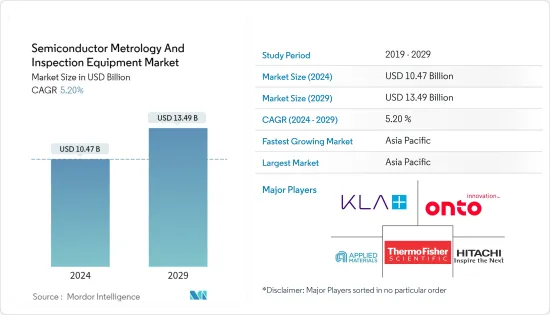
半导体计量和检测设备市场规模预计到 2024 年为 104.7 亿美元,预计到 2029 年将达到 134.9 亿美元,在预测期内(2024-2029 年)复合年增长率为 5.20%。
主要亮点
- 半导体计量和检测在半导体製造流程的管理中发挥重要作用。半导体晶圆製造过程大约涉及400至600个步骤,在一到两个月内完成。如果在流程的早期发现缺陷,则后续流程中投入的精力可能会被浪费。在半导体製造过程中,在关键时刻执行计量和检验程序,以确保特定的产量比率。
- Hamamatsu 强调实现高产量比率以满足当前半导体晶圆市场需求的重要性。计量和检测在各种半导体製造流程中发挥关键作用,以确保最佳的品质和产量比率。有效地表征和测量薄膜、线宽、图案缺陷和其他潜在缺陷对于快速解决任何问题并最大限度地减少代价高昂的停机时间至关重要。在半导体检测中,使用高强度紫外线光源对于缩短检测时间并提高评估晶圆上图案和薄膜的准确性至关重要。
- 半导体计量透过提供有关晶圆物理特性的详细资讯并促进调整製造流程以满足特定参数,在半导体製造过程中发挥重要作用。这确保了可靠、高品质的半导体装置的生产,同时最大限度地减少浪费,并保持製造过程的经济性和永续性。
- 半导体产业正在努力开发更紧凑的积体电路,提高性能和速度,因此製造技术也在不断进步。保持对程序的准确监控已成为製造中的基本要素。随着台积电、英飞凌、高通、英特尔等公司加大晶片生产投资,后端计量设备和服务的需求预计将增加。
- 智慧型手机、消费性电子产品和汽车应用推动了对具有成本效益的半导体材料的需求。这些进步正在刺激无线技术(5G)和人工智慧等创新。此外,随着物联网设备的采用趋势不断扩大,半导体产业预计将投资物联网设备以实现智慧产品。智慧型装置的使用正在不断增加,随着世界与 5G 的联繫更加紧密,预计这一数字将进一步增加。据GSMA称,到2025年,5G行动宽频连线预计将达到11亿,同年5G部署预计将覆盖全球34%的人口。
- 为了在市场上站稳脚跟,供应商正积极结成策略合作伙伴关係,打造先进的多功能测试平台。最近,k-Space Associates 于 2023 年 1 月宣布了其最新的薄膜测量工具 kSA XRF(X光萤光)。该工具专门设计用于精确测量无法使用光学方法可靠测量的薄膜厚度。其有效性已在各种基板(包括玻璃面板、晶圆和基座)上的半导体和介电层的测量中得到证明。这些应用在太阳能、发电和其他薄膜技术领域尤其重要。
- 然而,预测期内的市场成长预计将受到高设置成本和缺乏处理测量系统专业知识等因素的有效阻碍。为了克服这些挑战,服务型企业正在提供按需计量服务,并在精密尺寸计量专业领域提供专业扩展。
- 此外,研究市场的成长也受到美国贸易争端等宏观经济因素的挑战。美国对中国实施了多项制裁,阻止其获得先进的半导体设备。由于中国在市场供应链中发挥关键作用,这些发展将对市场的成长产生负面影响。
半导体测量和检测设备市场的趋势
晶圆检测取得显着成长
- 随着半导体装置设计变得越来越小,提高製造产量比率的挑战也变得更加突出。较小的节点和复杂的 3D架构的引入增加了设计阶段的步骤数量和复杂性。该过程有数百个步骤,任何阶段的缺陷或电气故障都可能破坏整体生产效率。鑑于上市时间和产量比率在决定新半导体设计成功与否的重要性,利用晶圆检测工具对于确保每个阶段的最佳性能至关重要。
- 未来几年,对3D积体电路的需求不断增长,预计将推动晶圆检测需求的成长。这些电路广泛应用于小型半导体装置,如记忆卡、智慧型手机、智慧卡和各种计算设备。 3D 电路已在许多空间受限的应用中变得流行,例如行动消费性电子产品、感测器、MEMS 和工业产品,因为它们提高了产品的整体性能,包括速度、耐用性、更低的功耗和更轻的内存。
- 经济云端处理解决方案的日益普及正在增加对微处理器和数位讯号处理器等逻辑装置的需求。这主要是由于各行业越来越多地使用伺服器和资料中心系统。此外,随着支援物联网的设备的激增,微处理器的使用也在增加。这些设备越来越多地利用薄晶圆来增强温度控制和优化性能。这些因素都有助于晶圆检测市场的扩大。
- 300mm晶圆在LED应用的广泛采用也是推动全球薄晶圆检测市场成长的因素。 300mm晶圆具有更高的产量比率,使LED製造商能够享受规模经济并提高盈利。随着运作中300毫米的晶圆生产设施数量持续增加,预计300毫米晶圆的需求将大幅增加。
- 根据SEMI硅製造商集团(SMG)年终分析,2023年全球硅晶圆出货量下降14.3%至126.02亿平方英吋。此外,同期晶圆收益下降 10.9%,至 123 亿美元。不过,人们对未来持乐观态度,2024 年的復苏势头预计将持续到 2026 年。由于人工智慧(AI)、高效能运算(HPC)、5G、汽车和工业应用等各领域对硅的需求增加,预计晶圆出货量将创下新高。
- 5G的引入以及5G部署活动投资的增加预计将进一步推动晶片产业对晶圆和晶圆检测工具的需求。根据爱立信 2022 年行动报告,预计未来五年北美将成为 5G 订阅采用率的全球领导者。预计到 2027 年,该地区 90% 的用户将是 5G。报告进一步预测,到2027年,西欧82%、波湾合作理事会80%、东北亚74%的用户将是5G。在已经开始引进5G的印度,预计到2027年5G将占所有合约的约40%。在全球范围内,到 2027 年,5G 预计将占所有订阅用户的近一半,订阅总合达到 44 亿。
- IT、物联网、可再生能源、电动车、电讯和其他产业将在未来几年显着成长。此外,这些领域严重依赖无线技术。 IC 和半导体的使用使得无线技术的应用成为可能。因此,晶圆检测市场存在着许多机会。英飞凌、台积电、意法半导体、美光、英特尔、三星等半导体行业知名企业都在晶片生产活动上投入巨资,为市场需求的成长做出了巨大贡献。
亚太地区主导市场
- 亚太地区无论是在製造或消费方面都是半导体产业的领先地区之一。根据SIA统计,亚太地区是最大的半导体市场,其中中国占最大份额。电子产业的显着进步,加上对电视和智慧型手机等电子设备的依赖增加,预计将推动该地区晶圆检查的需求。此外,位于该地区的公司愿意分配资金用于晶圆检查。
- 许多地区公司在半导体计量和检测设备市场建立了联盟和合作伙伴关係。例如,中国晶片製造设备製造商深圳精拓自动化设备有限公司与中国最大晶片开发商海思半导体(华为)签署了一份为期五年(2021-2025)具有法律约束力的谅解备忘录。两家公司的目标是扩大在半导体封装工具开发方面的合作伙伴关係,并创建一个自给自足且不受监管的行业。
- 地方政府发展当地半导体产业的措施也为所研究市场的成长创造了良好的前景。例如,中国国务院《国家积体电路产业发展指南》的目标是到2030年使中国在半导体产业的所有领域都处于世界领先地位。此外,「中国製造2025」倡议将先进半导体製造知识作为中国未来经济的重要组成部分。这非常强调建设强国製造策略。
- 例如,2023年7月,中国第二大晶片代工厂华虹半导体透露计画融资212亿元人民币(29.5亿美元)。这项策略措施符合中国实现半导体供应自给自足、克服美国技术封锁的决心。与前期主要以晶片生产为主不同,国家积体电路基金二期大力投资国内半导体製造、设备及相关材料,以克服现有障碍。
- 随着美国和中国之间的紧张局势持续,韩国正计划颁布自己版本的《晶片法案》以加强其半导体产业。这些紧张局势创造了对组装和包装等服务的需求,因此韩国支持其半导体产业至关重要。 2023 年 3 月,韩国国民议会通过了一项法案,透过对企业的税收优惠和投资激励措施来加强其主导的半导体产业。此类政府措施预计将为计量和测试等后端设备製造商创造更多机会,以扩大其在该地区的影响力。
- 2023年3月,韩国电子巨头三星宣布将在未来20年投资,支持韩国政府的倡议,即2042年在龙仁市南沙邑建立占地710万平方公尺的巨型半导体中心。韩元(相当于2308亿美元)。这项策略性倡议旨在加强韩国在竞争日益激烈的全球半导体市场中的地位,这将导致对晶圆测试、ATP 和其他设备等后端设备的需求增加。
- 此外,许多公司正致力于扩大业务,以增加各个领域的利润。新北市政府宣布,荷兰半导体设备专家ASML Holding NV将于2024年在新北市林口区开始兴建新厂。此外,日本电子及半导体公司东京电子株式会社正在台南市南科科学园区建立业务基地,预计于年终完工。这些投资有可能在计量和测试市场创造商机。
半导体测量和检测设备产业概况
半导体计量和测试设备市场由知名企业组成,例如:应用材料公司、尼康计量公司和 KLA 公司透过专注于市场扩张和收购活动,有效地推动了所研究的市场的整体成长。创新。
- 2023 年 12 月,日立高新科技公司发布了其暗场晶圆缺陷检测设备的最新创新产品 DI4600。这种最先进的工具专门设计用于检查半导体生产线上图案化晶圆上的颗粒和缺陷。 DI4600配备专用伺服器,增强了资料处理能力,提高了颗粒和缺陷检测能力。半导体製造商可以将这种先进的系统纳入其生产线,以执行高精度的缺陷监控,随着产量的增加,提高产量比率并提高成本效率。
- 2023 年 7 月,应用材料公司宣布与弗劳恩霍夫 IPMS(光子微系统研究所)进行开创性合作,在欧洲建立首屈一指的半导体计量和製程分析技术中心。该创新中心将加速半导体研究,并加强与欧洲各地晶片製造商和生态系统合作伙伴的研发活动,重点关注ICAPS(物联网、通讯、汽车、电源和感测器)市场领域,旨在提供尖端技术。系统。
其他福利:
- Excel 格式的市场预测 (ME) 表
- 3 个月分析师支持
目录
第一章简介
- 研究假设和市场定义
- 调查范围
第二章调查方法
第三章执行摘要
第四章市场洞察
- 市场概况
- 产业吸引力-波特五力分析
- 供应商的议价能力
- 买方议价能力
- 新进入者的威胁
- 替代品的威胁
- 竞争程度
- 评估主要宏观趋势的影响
第五章市场动态
- 市场驱动因素
- 对高性能、低成本半导体的需求不断增长
- 消费性电子产品对半导体晶圆的需求增加
- 市场限制因素
- 设置成本高且缺乏有效处理测量系统的专业知识
- 原料和製造成本高
第六章 市场细分
- 按类型
- 微影测量
- 覆盖
- 尺寸测量装置
- 掩模检查/测量
- 晶圆检查
- 薄膜测量
- 其他过程控制系统
- 微影测量
- 按地区
- 北美洲
- 欧洲
- 亚太地区
- 世界其他地区
第七章 竞争格局
- 公司简介
- KLA Corporation
- Applied Materials Inc.
- Onto Innovation Inc.
- Thermo Fisher Scientific Inc.
- Hitachi Hi-Technologies Corporation(Hitachi Limited)
- Nova Measuring Instruments Ltd
- ASML Holding NV
- Lasertec Corporation
- JEOL Ltd
- Nikon Metrology NV(Nikon Group)
- Camtek Limited
第八章投资分析
第9章市场的未来
The Semiconductor Metrology And Inspection Equipment Market size is estimated at USD 10.47 billion in 2024, and is expected to reach USD 13.49 billion by 2029, growing at a CAGR of 5.20% during the forecast period (2024-2029).
Key Highlights
- Semiconductor metrology and inspection play a crucial role in the management of the semiconductor manufacturing process. The manufacturing process of semiconductor wafers involves approximately 400 to 600 steps, which can be completed within one to two months. Any shortcomings detected early on in the process can result in the wastage of all the efforts put into the subsequent steps. Metrology and inspection procedures are implemented at critical junctures of the semiconductor manufacturing process to guarantee a specific yield.
- Hamamatsu emphasizes the importance of achieving high production yields in order to satisfy the current market requirements for semiconductor wafers. Metrology and inspection play a vital role in the extensive semiconductor manufacturing process to guarantee optimal quality and yield. It is crucial to efficiently characterize and measure thin films, line widths, pattern flaws, and other possible defects to promptly address any issues and minimize expensive downtime. In semiconductor inspection, the utilization of higher radiance UV light sources is essential to reduce inspection durations and improve the precision of evaluating patterns and thin films on wafers.
- Semiconductor metrology plays a crucial role in the semiconductor manufacturing process by offering detailed information on the physical properties of the wafer and facilitating adjustments to the production process to meet specific parameters. This ensures the production of reliable semiconductor devices of high quality while minimizing wastage, thus maintaining the economic viability and sustainability of the manufacturing process.
- The semiconductor sector is continuously aiming for more compact integrated circuits that provide enhanced performance and speeds, resulting in progress in manufacturing techniques. Maintaining accurate oversight of procedures has emerged as a vital factor in manufacturing. With firms like TSMC, Infineon, Qualcomm, and Intel expanding their chip production investments, the demand for metrology equipment and services is expected to rise in the back-end process.
- The demand for cost-effective semiconductor materials is being fueled by smartphones, consumer electronics, and automotive applications. These advancements are inspiring innovations like wireless technologies (5G) and artificial intelligence. Additionally, the semiconductor industry is expected to invest in IoT devices to achieve smart products as the trend of adoption of IoT devices continues to grow. The utilization of smart devices is on the rise and is anticipated to increase further with the global expansion of 5G connections. As per the GSMA, it is estimated that 5G mobile broadband connections will reach 1,100 million (1.1 billion) by the year 2025, while the 5G deployment is expected to encompass 34% of the global population by the same year.
- In order to gain a strong foothold in the market, vendors are actively engaging in strategic partnerships to create advanced multifunction inspection platforms. Recently, k-Space Associates introduced its latest thin film metrology tool, the kSA XRF (X-ray fluorescence), in January 2023. This tool is specifically designed to accurately measure the thickness of films that cannot be reliably measured using optical methods. Its effectiveness has been demonstrated in measuring semiconductor and dielectric layers on various substrates such as glass panels, wafers, and susceptors. These applications are particularly relevant in the fields of solar energy, power generation, and other thin-film technologies.
- However, the market's growth during the forecast period is expected to be hindered efficiently by factors such as high setup costs and a lack of expertise in handling metrology systems. In order to overcome these challenges, service-oriented players are offering on-demand metrology services, providing a professional extension in the specialized field of precision dimensional metrology.
- Furthermore, the growth of the market studied is also challenged by macroeconomic factors, such as the US-China trade dispute. The United States has imposed several sanctions on China, preventing the country from accessing advanced semiconductor equipment. Since China plays a significant role in the market's supply chain, these trends negatively impact the growth of the market studied.
Semiconductor Metrology and Inspection Equipment Market Market Trends
Wafer Inspection to Witness Significant Growth
- As the design of semiconductor devices progresses toward smaller nodes, the challenge of increasing manufacturing yields becomes more pronounced. The introduction of smaller nodes and intricate 3D architectures leads to additional steps and heightened complexity in the design phase. With hundreds of steps in the process, any defect or electrical fault at any stage can impede overall production efficiency. Given the significance of time-to-market and time-to-yield in determining the success of a new semiconductor design, the utilization of wafer inspection tools is crucial to ensure optimal performance at each stage.
- The growing demand for wafer inspection is expected to be fueled by the increasing need for three-dimensional integrated circuits in the upcoming years. These circuits are widely used in small semiconductor devices such as memory cards, smartphones, smart cards, and various computing devices. Three-dimensional circuits are gaining popularity in numerous space-constrained applications like portable consumer electronics, sensors, MEMS, and industrial products, as they enhance overall product performance in terms of speed, durability, low power consumption, and lightweight memory.
- The increasing availability of cost-effective cloud computing solutions has led to a rise in demand for logic devices such as microprocessors and digital signal processors. This is primarily driven by the growing use of server and data center systems in various industries. Furthermore, the proliferation of IoT-enabled devices has resulted in a higher usage of microprocessors. Thin wafers are increasingly utilized in these devices to enhance temperature control and optimize performance. These factors collectively contribute to the expansion of the wafer inspection market.
- The widespread adoption of 300 mm wafers in LED applications is also a key driver for the global growth of the thin wafer inspection market. These wafers offer higher yields, enabling LED manufacturers to achieve economies of scale and enhance profitability. As the number of operational 300 mm wafer production facilities continues to increase, the demand for 300 mm wafers is expected to witness a significant surge.
- According to the year-end analysis conducted by the SEMI Silicon Manufacturers Group (SMG), global silicon wafer shipments experienced a decline of 14.3% in 2023, reaching 12,602 million square inches. Additionally, wafer revenue contracted by 10.9% to USD 12.3 billion during the same period. However, there is optimism for the future as the momentum from the 2024 rebound is expected to continue until 2026. This positive trend is anticipated to result in new record-high wafer shipments, driven by the increasing demand for silicon in various sectors such as artificial intelligence (AI), high-performance computing (HPC), 5G, automotive, and industrial applications.
- The introduction of 5G and increasing investments in the 5G adoption activities are further expected to drive the demand for wafers and wafer inspection tools in the chip industry. According to the Ericsson Mobility Report 2022, North America is projected to be the global leader in 5G subscription penetration over the next five years. It is anticipated that 90% of subscriptions in the region will be 5G by 2027. Additionally, the report predicts that by 2027, 82% of subscriptions in Western Europe, 80% in the Gulf Cooperation Council, and 74% in North-East Asia will be 5G. In India, where 5G deployments have already begun, it is expected that 5G will account for approximately 40% of all subscriptions by 2027. Globally, 5G is expected to represent nearly half of all subscriptions by 2027, reaching a total of 4.4 billion subscriptions.
- The IT, IoT, renewable, EVs, telecom, and other sectors are poised for substantial growth in the upcoming years. Additionally, these sectors heavily rely on wireless technology. The utilization of ICs and semiconductors enables the application of wireless technology. As a result, the wafer inspection market is presented with a multitude of opportunities. Prominent companies in the semiconductor industry, such as Infineon, TSMC, ST, Micron, Intel, Samsung, and others, are making significant investments in chip production activities, which can greatly contribute to the market's increased demand.
Asia-Pacific to Dominate the Market
- Asia-Pacific is one of the prominent regions in the semiconductor industry in terms of manufacturing and consumption. According to SIA, Asia-Pacific is the largest regional semiconductor market, and China accounts for the most significant share in the region. The significant advancements in the electronics sector, combined with the growing reliance on electronic gadgets like televisions and smartphones, are anticipated to boost the requirement for wafer inspection in the region. Furthermore, companies situated in this area are prepared to allocate funds toward the utilization of wafer inspections.
- Many regional companies are entering collaborations and partnerships in the semiconductor metrology/inspection equipment market. For instance, Shenzhen JT Automation Equipment, a chip production tool manufacturer in China, announced a legally binding five-year (2021-2025) memorandum of understanding with Huawei's HiSilicon Technologies, China's largest chip developer. Both firms aim to extend their partnership for the development of semiconductor packaging tools, creating a self-sufficient and regulated industry.
- The regional government's initiatives to develop the local semiconductor industry also create a favorable outlook for the growth of the market studied. For instance, China's State Council's "National Integrated Circuit Industry Development Guidelines" aim to make the country a global leader in all segments of the semiconductor industry by 2030. Additionally, the Made in China 2025 initiative maintains achieving knowledge concerning advanced semiconductor manufacturing as a vital component of China's future economy. It is highly focused on building a strategy for strong manufacturing nationwide.
- For instance, in July 2023, Hua Hong Semiconductor, the second-largest chip foundry in China, revealed its plan to raise CNY 21.2 billion (USD 2.95 billion). This strategic move is in line with China's determined efforts to attain self-sufficiency in semiconductor supply and overcome the technology blockade imposed by the United States. In contrast to the initial phase that primarily concentrated on chip production, the China IC Fund II has made significant investments in domestic semiconductor manufacturing, equipment, and associated materials to overcome the existing obstacles.
- South Korea plans to enact its own version of the "Chips Act" in order to bolster its semiconductor industry amid the ongoing tensions between the United States and China. These tensions have created a demand for services such as assembly and packaging, making it crucial for South Korea to support its semiconductor industry. In March 2023, the country's parliament passed legislation to strengthen its dominant semiconductor industry by providing tax benefits to businesses and encouraging investments. Such government initiatives are expected to boost the opportunities for the backend equipment markers, such as metrology and inspection, to enhance their presence in the region.
- In March 2023, Samsung, the Korean electronics giant, announced its intention to invest KRW 300 trillion (equivalent to USD 230.8 billion) over the next two decades in support of the South Korean government's initiative to establish a massive semiconductor hub spanning 7.1 million square meters in Namsayup, Yongin, by 2042. This strategic move is designed to bolster Korea's position in the increasingly competitive global semiconductor market, consequently driving up the demand for backend equipment such as wafer testing, ATP, and other equipment.
- Additionally, numerous enterprises are focusing on expanding their activities to boost profits in different sectors. The New Taipei City government announced that ASML Holding NV, a Dutch company that specializes in semiconductor equipment, will commence the construction of its new facility in the Linkou District of New Taipei City in the fiscal year 2024. Moreover, Tokyo Electron Ltd, a Japanese electronics and semiconductor corporation, is making progress in establishing its operations hub in the Southern Taiwan Science Park in Tainan, with plans to complete it by the end of 2024. These investments have the potential to create opportunities in the metrology and inspection market.
Semiconductor Metrology and Inspection Equipment Industry Overview
The semiconductor metrology and inspection equipment market comprises prominent players such as Applied Materials Inc., Nikon Metrology NV, and KLA Corporation. These firms have continuously expanded their operation scales by focusing on market expansions and acquisitions. Acquisition activities effectively set the ball rolling regarding the overall growth of the market studied. Large companies have also been expending significant resources on R&D operations to protect their market position and drive innovation in the market studied. Overall, the degree of competition remains high, primarily driven by the strong presence of prominent players involved in the market studied.
- In December 2023, Hitachi High-Tech Corporation unveiled the DI4600, the latest innovation in its Dark Field Wafer Defect Inspection System. This state-of-the-art tool is specifically designed to inspect particles and defects on patterned wafers in semiconductor production lines. With its dedicated server, the DI4600 offers enhanced data processing power, enabling improved detection capabilities for particles and defects. By incorporating this advanced system into their production lines, semiconductor manufacturers can ensure highly accurate defect monitoring, resulting in increased yields and cost efficiency as production volumes continue to rise.
- In July 2023, Applied Materials Inc. and the Fraunhofer Institute for Photonic Microsystems IPMS announced a pioneering collaboration to create the premier technology center for semiconductor metrology and process analysis in Europe. This innovative hub is designed to provide state-of-the-art metrology systems to accelerate semiconductor research and enhance development efforts with chipmakers and ecosystem partners across Europe, with a specific focus on ICAPS (Internet of Things, communications, automotive, power, and sensors) market segments.
Additional Benefits:
- The market estimate (ME) sheet in Excel format
- 3 months of analyst support
TABLE OF CONTENTS
1 INTRODUCTION
- 1.1 Study Assumptions and Market Definition
- 1.2 Scope of the Study
2 RESEARCH METHODOLOGY
3 EXECUTIVE SUMMARY
4 MARKET INSIGHTS
- 4.1 Market Overview
- 4.2 Industry Attractiveness - Porter's Five Forces Analysis
- 4.2.1 Bargaining Power of Suppliers
- 4.2.2 Bargaining Power of Buyers
- 4.2.3 Threat of New Entrants
- 4.2.4 Threat of Substitutes
- 4.2.5 Degree of Competition
- 4.3 An Assessment of the Impact of Key Macro Trends
5 MARKET DYNAMICS
- 5.1 Market Drivers
- 5.1.1 Increasing Demand for High-performance, Low-cost Semiconductors
- 5.1.2 Increasing Demand for Semiconductor Wafers in Consumer Electronics
- 5.2 Market Restraints
- 5.2.1 High Setup Cost and Lack of Expertise in Handling Metrology Systems Efficiently
- 5.2.2 High Raw Material and Fabrication Costs
6 MARKET SEGMENTATION
- 6.1 By Type
- 6.1.1 Lithography Metrology
- 6.1.1.1 Overlay
- 6.1.1.2 Dimension Equipment
- 6.1.1.3 Mask Inspection and Metrology
- 6.1.2 Wafer Inspection
- 6.1.3 Thin Film Metrology
- 6.1.4 Other Process Control Systems
- 6.1.1 Lithography Metrology
- 6.2 By Geography
- 6.2.1 North America
- 6.2.2 Europe
- 6.2.3 Asia-Pacific
- 6.2.4 Rest of the World
7 COMPETITIVE LANDSCAPE
- 7.1 Company Profiles
- 7.1.1 KLA Corporation
- 7.1.2 Applied Materials Inc.
- 7.1.3 Onto Innovation Inc.
- 7.1.4 Thermo Fisher Scientific Inc.
- 7.1.5 Hitachi Hi-Technologies Corporation (Hitachi Limited)
- 7.1.6 Nova Measuring Instruments Ltd
- 7.1.7 ASML Holding NV
- 7.1.8 Lasertec Corporation
- 7.1.9 JEOL Ltd
- 7.1.10 Nikon Metrology NV (Nikon Group)
- 7.1.11 Camtek Limited
8 INVESTMENT ANALYSIS
9 FUTURE OF THE MARKET
 曲线追踪器市场报告:趋势、预测和竞争分析(至 2031 年)
 半导体计量和测试市场按类型、技术类型、组件类型、最终用户、应用和行业细分 - 2025-2030 年全球预测
 2025 年全球半导体计量和测试市场报告
 半导体计量及检测市场机会、成长动力、产业趋势分析及 2025-2034 年预测半导体计量和检测系统市场,按类型、技术、组织规模、应用、国家和地区 - 2024-2032 年行业分析、市场规模、市场份额和预测
 半导体测量·检验的全球市场 - 主要趋势与机会(~2029年)半导体计量设备市场 - 2023-2031 年全球行业分析、规模、份额、增长、趋势和预测