


 |
市场调查报告书
商品编码
1641959
晶圆清洗设备:市场占有率分析、产业趋势与统计、成长预测(2025-2030 年)Wafer Cleaning Equipment - Market Share Analysis, Industry Trends & Statistics, Growth Forecasts (2025 - 2030) |
||||||
※ 本网页内容可能与最新版本有所差异。详细情况请与我们联繫。
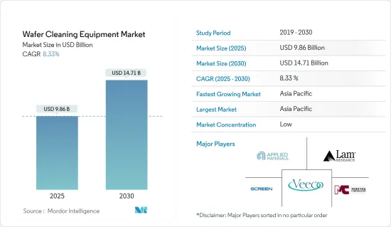
晶圆清洗设备市场规模预计在 2025 年为 98.6 亿美元,预计到 2030 年将达到 147.1 亿美元,预测期内(2025-2030 年)的复合年增长率为 8.33%。
随着电子元件需求的增加以及使电子封装更加资源高效的措施,晶圆清洗设备被广泛应用于各种领域。
关键亮点
- 智慧、相容设备和支援网路的日益普及是全球晶圆清洗设备市场发展的主要驱动力。例如,2022 年 6 月,DISH 宣布将在 Project Genesis 首次推出仅 42 天后将其扩展至美国20% 以上的人口(全美 120 个城市)。这意味着联邦通信委员会的临时期限已经满足。此网路高度发展、完全云端原生,并依赖开放式 RAN 架构。
- 此外,印刷电子的日益普及、半导体装置产业对升级和提高半导体产品品质和生产标准的日益重视也是支持晶圆清洗设备市场发展的突出因素。
- 2022年6月,NEO Battery Materials Ltd.与韩国印刷电路基板生产公司Automobile & PCB Inc.签署了战略谅解备忘录(MoU)。透过此次合作,两家公司将利用 NEO 的技术专长以及 A&P 的附属公司 YSP 和 Yongsan 已建立的网路来加强 NEO 的全球业务网络。此类产品开发活动可能会进一步推动印刷电子产品的成长并产生市场发展的需求。
- 预计对硅基感测器的需求不断增加将为市场扩张提供有利的潜力。此外,一些供应商已经在致力于增加SiC晶圆的产量。例如,2023年8月,英飞凌科技股份公司宣布计划扩建其在马来西亚的製造工厂并建立一座200毫米SiC晶圆厂。这些发展显示对晶圆转型的需求不断增长。
- 此外,Cree(Wolfspeed)还在增加 Wolfspeed 品牌功率和射频半导体的生产能力,随着该公司出售其照明业务以专注于 SiC 和 GaN 产品,该产能还在继续增长。为了满足电动车、工业市场和行动通讯领域的高需求,Cree 正在纽约建造一座价值 12 亿美元的 200 毫米晶圆厂,并计划于 2022 年开始生产。
- 生产这些材料的一个主要挑战是环境管理。晶圆清洗过程会产生灰尘和生物危害废弃物,如果不妥善处理,将对气候产生直接影响。因此,政府制定了各种法规来研究如何处理和避免此类问题。此外,对熟练劳动力的需求以及严格且不断变化的品质标准阻碍了市场的成长。
晶圆清洗设备的市场趋势
智慧型手机和平板电脑推动市场成长
- 智慧型手机和平板电脑等家用电子电器的使用日益增多,刺激了晶圆清洗设备市场的成长。新技术的出现以及消费者对更先进的智慧型手机和平板设备日益增长的需求,极大地推动了该行业的成长速度。例如,根据爱立信预测,到2027年全球智慧型手机用户数量将达到78.4亿。
- 平板电脑和智慧型手机市场的快速成长增加了对半导体晶圆的需求,进而导致对晶圆清洗设备的需求增加。据印度手机与电子协会 (ICEA) 称,预计到 2025 年,印度的笔记型电脑和平板电脑製造业产值将达到 1,000 亿美元。此外,预计到 2026 财年,印度行动电话市场的销售额将达到 2.4 兆印度卢比(293.8 亿美元)。
- 由于现在大多数任务都可以透过智慧型手机完成,包括电子邮件、社群媒体、游戏和聊天,因此对智慧型手机的需求正在增加,而个人电脑的销售正在下降。根据GSMA预测,到2025年,智慧型手机连线数将达到约75亿,占行动连线的五分之四以上。
- 智慧型手机技术正在发展,影响消费者的日常行销策略、商业活动和生活方式。智慧型手机技术的接受度是当今科技成功的关键因素。因此,确定影响消费者对智慧型手机技术行为的关键因素具有重要价值。
- 根据IBEF报道,三星宣布计画未来5年在印度投资3.7兆卢比(500亿美元)用于生产行动电话。该公司还计划根据 PLI 计划生产价值 2.2 兆印度卢比(300 亿美元)的行动电话,每部价格超过 15,000 印度卢比(200 美元)。智慧型手机和平板电脑等家用电子电器产品的扩张可能会进一步推动对晶圆清洗设备的需求。
亚太地区市场显着成长
- 亚太地区已成为最大的半导体市场。数位技术的渗透、快速的都市化和工业化正在促进这一成长。此外,大型半导体製造、封装和组装产业的存在也为该地区晶圆设备市场的发展创造了有利的条件。
- 此外,中国不仅是亚太地区,也是世界上最大的半导体中心。据半导体产业协会称,中国近期以 1,925 亿美元的晶片总销售额领先半导体市场,与前一年同期比较成长 27.1%。中国也吸引了领先晶片製造商的巨额投资,透过建立新工厂来扩大晶片产量。此外,WSTS 预测 2022 年全球销售额将达到 5,730 亿美元。
- 此外,受电动车产业需求不断增长的推动,日本企业正在大力投资提高碳化硅功率半导体的产量。例如,总部位于东京的昭和电工株式会社于2022年3月开始量产直径6吋(150毫米)的结晶单晶晶片(SiC晶片)。
- 由于消费性电子和半导体产业的不断发展,亚太地区是主要的半导体晶圆清洗市场之一。对小型、智慧和便携式设备日益增长的需求正在支撑该地区市场的成长。根据 IBEF 预测,印度家用电子电器(ACE) 市场将以 9% 的复合年增长率成长,到 2022 年达到 3.15 兆印度卢比(483.7 亿美元)。此外,2022年9月,印度月度行动电话出口额首次突破10亿美元大关。
- 受冠状病毒大流行推动的居家隔离趋势继续推动对半导体晶片的需求。例如,根据WSTS的数据,预计2023年亚太半导体产业的销售额将超过4,000亿美元。这些趋势正在鼓励主要设备製造商进入亚太市场。
- 例如,市场上最知名的供应商之一 ASML 最近在台湾台南开设了一个最先进的培训设施。该地区上述的扩张可能会在预测期内进一步增加对晶圆清洗设备的需求。
晶圆清洗设备产业概况
晶圆清洗设备市场高度分散,主要企业包括 Lam Research Corporation、Applied Materials Inc.、Veeco Instruments、Tokyo Electron Ltd.、Entegris、Modutek 和 Semes。这些参与企业的市占率较大,且信誉度较高,因而带动了市场整合。
- 2024年3月:利用「精密流体模拟」等技术,开发出满足日益小型化的半导体製造最清洗节点需求的晶圆,并以优异的清洗干燥性能实现卓越的生产率和高产量。设备荣获大河内财团法人第70届大河内纪念生产奖。
- 2023 年 10 月 - SCREEN SPE 将引入 FTD Solutions Inc. 的 WMA(水管理应用程式),以实现水资源管理的可视化,从而加速永续发展。作为世界顶级的半导体清洗设备製造商,该系统使用水,我们正在加快开创性的努力,以减少对环境的影响。
其他福利
- Excel 格式的市场预测 (ME) 表
- 3 个月的分析师支持
目录
第 1 章 简介
- 调查结果
- 调查前提
- 研究范围
第二章调查方法
第三章执行摘要
第四章 市场动态
- 市场概况
- 采用市场驱动因素与限制因素
- 市场驱动因素
- 平板电脑和智慧型手机的需求不断增长
- 半导体产业的成长
- 市场限制
- 晶圆清洗过程中产生的有害化学物质和气体相关的环境问题
- 产业价值链分析
- 产业吸引力-波特五力分析
- 新进入者的威胁
- 买家的议价能力
- 供应商的议价能力
- 替代品的威胁
- 竞争对手之间的竞争
第五章 技术简介
- 单波喷雾系统
- 单晶圆低温系统
- 大量浸泡清洗系统
- 批量喷淋清洗系统
- 洗涤器
第六章 市场细分
- 依运作方式类型
- 自动装置
- 半自动设备
- 手动操作
- 按应用
- 智慧型手机和平板电脑
- 储存装置
- 射频设备
- LED
- 其他的
- 按地区
- 北美洲
- 美国
- 加拿大
- 欧洲
- 德国
- 法国
- 义大利
- 英国
- 亚洲
- 中国
- 日本
- 台湾
- 韩国
- 澳洲和纽西兰
- 拉丁美洲
- 中东和非洲
- 北美洲
第七章 竞争格局
- 公司简介
- Applied Materials, Inc.
- Lam Research Corporation
- Veeco Instruments Inc.
- Screen Holdings Co., Ltd
- Modutek Corporation
- Entegris, Inc
- PVA Tepla AG
第八章投资分析
第九章:市场的未来
The Wafer Cleaning Equipment Market size is estimated at USD 9.86 billion in 2025, and is expected to reach USD 14.71 billion by 2030, at a CAGR of 8.33% during the forecast period (2025-2030).
Due to the massive demand for electronic components owing to amplified usage, the increasing measures to make electronic packaging highly resourceful have made wafer-cleaning equipment used in myriad applications.
Key Highlights
- The growth in adopting smart and compatible devices and feasible networks is significantly aiding the development of the global wafer-cleaning equipment market. For instance, in June 2022, DISH informed that Project Genesis would be expanded to over 20% of the US population (in 120 cities across the USA) only 42 days after the initial launch. As such, it just met the FCC's interim deadline. The network is very developed, completely cloud-native, and reliant on Open RAN architecture.
- Furthermore, the increasing penetration of printed electronics and rising concern for upgrading and improving the semiconductor product quality and production standards in the semiconductor devices industry are some prominent factors behind the development of the Wafer Cleaning Equipment Market.
- In June 2022, NEO Battery Materials Ltd. signed a strategic Memorandum of Understanding (MoU) with Automobile & PCB Inc., a Korean company manufacturing printed circuit boards. Through this collaboration, both players will leverage NEO's technical expertise and the reputable and recognized network of A&P's related companies, YSP and Yongsan, to strengthen NEO's business network globally. Such activities for product development may further drive the growth of printed electronics, creating demand for studied market growth.
- An increase in demand for silicon-based sensors is anticipated to deliver lucrative possibilities for market expansion. Further, some vendors are already working toward increasing the production of SiC wafers. For instance, in August 2023, Infineon Technologies AG announced its plans to expand its manufacturing facility in Malaysia to establish 200 mm SiC fab. Such developments indicate the growing demand for wafer transition.
- Furthermore, Cree (Wolfspeed) is also elevating its production capacity for its Wolfspeed brand of power and radio frequency semiconductors, an ongoing strategy that grew when the company sold its lighting business to focus on SiC and GaN products. To meet the high demand in EVs, industrial markets, and mobile telecommunications, Cree is building a USD 1.2 billion 200mm SiC wafer fab in New York, where production began in 2022.
- The major challenge for the production of these materials is to control the environment, especially in the process of wafer cleaning, especially dust and biohazard waste are generated, which have a direct impact on the climate if they are not appropriately treated. Therefore different government regulations are made to consider how they must be handled to avoid such problems. Moreover, the need for a skilled workforce and strict and changing quality standards hinder the market growth.
Wafer Cleaning Equipment Market Trends
Smartphones & Tablets to Drive the Market Growth
- The increase in the usage of consumer electronic devices such as smartphones and tablets has stimulated the growth of the wafer-cleaning equipment market. Emerging new technologies and growth in consumer demand for more advanced smartphones and tablets have boosted the growth pace of the industry to a great extent. For instance, according to Ericsson, the global number of smartphone subscribers is anticipated to reach 7,840 million by 2027.
- The enormous growth in the tablets and smartphones market has raised the need for semiconductor wafers, thus raising the demand for wafer-cleaning equipment. According to India Cellular & Electronics Association (ICEA), India is anticipated to acquire a value of USD 100 billion in manufacturing laptops and tablets by 2025. In addition, the Indian mobile phone market is expected to generate INR 2.4 trillion (USD 29.38 billion) in revenue by FY2026.
- The demand for smartphones has increased, and PC sales have declined because most tasks, such as emailing, social media, gaming, and chatting, can now be done via smartphones. According to GSMA, there will be about 7.5 billion smartphone connections by 2025, accounting for above four in five mobile connections.
- Smartphone technology is developing to influence the consumer's daily marketing strategies, business activities, and lifestyle. The acceptance of smartphone technology is a crucial factor in the success of today's technology. Due to this, identifying the main factors that influence the consumer's behavior toward smartphone technology is extremely valuable.
- According to IBEF, Samsung announced plans to invest INR 3.7 lakh crore (USD 50 billion) in India over the next five years to manufacture phones. It plans to produce phones worth INR 2.2 lakh crore (USD 30 billion), priced above INR 15,000 (USD 200), under the PLI scheme. Such expansion in consumer electronics such as smartphones and tablets may further drive the demand for Wafer Cleaning equipment.
Asia Pacific to Experience Significant Market Growth
- Asia Pacific region has appeared as the largest semiconductor market. The growing penetration of digital technologies, rapid urbanization, and industrialization contribute to this growth. Additionally, the presence of large semiconductor manufacturing, packaging, and assembly industries also creates a favorable scenario for developing the wafer equipment market in the region.
- In addition, China is the largest semiconductor hub not only in Asia-Pacific but also in the world. As per Semiconductor Industry Association, China recently led the semiconductor market with total chip sales of USD 192.5 billion, marking an expansion of 27.1 percent year on year. The country also draws huge investments from significant chipmakers to extend chip production by launching new facilities. Further, in 2022, WSTS forecasted global sales totaled USD 573 billion.
- Furthermore, Japanese companies are creating heavy investments to improve the production of SiC power semiconductors driven by the increased demand from the EV industry. For instance, in March 2022, Tokyo-headquartered Showa Denko KK introduced the mass production of silicon carbide single crystal wafers (SiC wafers) with a diameter of 6 inches (150 mm), which are used as materials for SiC epitaxial wafers to be processed and installed into SiC power semiconductors.
- Asia-Pacific is one of the vital semiconductor wafer cleaning markets owing to the presence of the ever-growing consumer electronics and semiconductor industries. The rise in demand for small and smart portable devices supplements the market growth in the region. According to IBEF, India's consumer electronics (ACE) market increased at 9 percent CAGR to reach INR 3.15 trillion (USD 48.37 billion) in 2022. Furthermore, in September 2022, monthly mobile phone exports from India crossed the USD 1 billion mark for the first time.
- The stay-at-home trend spurred by the coronavirus pandemic continues to drive the demand for semiconductor chips. For instance, according to WSTS, the estimated semiconductor industry revenue in the Asia Pacific region is expected to reach over USD 400 billion in 2023. Such trends encourage leading equipment manufacturers to enter the Asia Pacific (APAC) market.
- For instance, ASML, one of the most prominent vendors in the market, recently opened a new state-of-the-art training facility in Tainan, Taiwan. The above expansion in the region may further create demand for the Wafer Cleaning Equipment in the forecasted period.
Wafer Cleaning Equipment Industry Overview
The Wafer Cleaning Equipment Market is quite fragmented, with the major players in the studied market such as Lam Research Corporation, Applied Materials, Inc., Veeco Instruments Inc., Tokyo Electron Limited, Entegris, Inc, Modutek Corporation, Semes Co., Ltd., among others. These players account for a significant share and are reliable, leading to higher market consolidation.
- March 2024 - SCREEN Holdings Co. and SCREEN Semiconductor Solutions Co., Ltd. have received the Okochi Memorial Production Prize during the 70th annual award ceremony sponsored by the Okochi Foundation as their wafer cleaning equipment accommodates the advanced nodes in increasingly miniaturized semiconductor manufacturing by leveraging precise fluid simulation and other technologies, which bring about excellent cleaning and drying performance, as well as outstanding productivity supported by high throughput.
- October 2023 -SCREEN SPE introduced FTD solutions INC's Water Management Application (WMA) to visualize water management to accelerate sustainability development. As the company with the top global market share for semiconductor cleaning systems, which are systems that deal with water, we will accelerate advanced initiatives to reduce the environmental impact.
Additional Benefits:
- The market estimate (ME) sheet in Excel format
- 3 months of analyst support
TABLE OF CONTENTS
1 INTRODUCTION
- 1.1 Study Deliverables
- 1.2 Study Assumptions
- 1.3 Scope of the Study
2 RESEARCH METHODOLOGY
3 EXECUTIVE SUMMARY
4 MARKET DYNAMICS
- 4.1 Market Overview
- 4.2 Introduction to Market Drivers and Restraints
- 4.3 Market Drivers
- 4.3.1 Growing Demand for Tablets and Smartphones
- 4.3.2 Growth in the Semiconductor Industry
- 4.4 Market Restraints
- 4.4.1 Environmental Concerns Related to Hazardous Chemicals and Gases Generated During Wafer Cleaning Process
- 4.5 Industry Value Chain Analysis
- 4.6 Industry Attractiveness - Porter's Five Forces Analysis
- 4.6.1 Threat of New Entrants
- 4.6.2 Bargaining Power of Buyers
- 4.6.3 Bargaining Power of Suppliers
- 4.6.4 Threat of Substitute Products
- 4.6.5 Intensity of Competitive Rivalry
5 TECHNOLOGY SNAPSHOT
- 5.1 Single-wafer Spray Systems
- 5.2 Single-wafer Cryogenic Systems
- 5.3 Batch Immersion Cleaning Systems
- 5.4 Batch Spray Cleaning Systems
- 5.5 Scrubbers
6 MARKET SEGMENTATION
- 6.1 By Operating Mode Type
- 6.1.1 Automatic Equipment
- 6.1.2 Semi-automatic Equipment
- 6.1.3 Manual Equipment
- 6.2 By Application
- 6.2.1 Smartphones & Tablets
- 6.2.2 Memory Devices
- 6.2.3 RF Device
- 6.2.4 LED
- 6.2.5 Other Applications
- 6.3 By Geography
- 6.3.1 North America
- 6.3.1.1 United States
- 6.3.1.2 Canada
- 6.3.2 Europe
- 6.3.2.1 Germany
- 6.3.2.2 France
- 6.3.2.3 Italy
- 6.3.2.4 United Kingdom
- 6.3.3 Asia
- 6.3.3.1 China
- 6.3.3.2 Japan
- 6.3.3.3 Taiwan
- 6.3.3.4 South Korea
- 6.3.4 Australia and New Zealand
- 6.3.5 Latin America
- 6.3.6 Middle East and Africa
- 6.3.1 North America
7 COMPETITIVE LANDSCAPE
- 7.1 Company Profiles
- 7.1.1 Applied Materials, Inc.
- 7.1.2 Lam Research Corporation
- 7.1.3 Veeco Instruments Inc.
- 7.1.4 Screen Holdings Co., Ltd
- 7.1.5 Modutek Corporation
- 7.1.6 Entegris, Inc
- 7.1.7 PVA Tepla AG
8 INVESTMENT ANALYSIS
9 FUTURE OF THE MARKET
 晶圆清洗设备市场(按设备类型、晶圆尺寸、杂质、应用和最终用户产业)—全球预测 2025-2032
 全球FOUP清洗机市场、绩效及预测(2020-2031年)
 全球威化蛋筒(冰淇淋甜筒)市场
 2025年全球晶圆清洗设备市场报告
 硅晶圆清洗解决方案市场报告:趋势、预测与竞争分析(至 2031 年)
 半导体晶圆清洗设备市场规模、份额、成长分析,依设备类型、晶圆尺寸、技术、营运模式、地区 - 产业预测,2025-2032
 全球晶圆清洁设备市场(2024年)
 威化甜筒的全球市场:类型·各口味·类别·购买诉求·终端用户·流通管道的预测 (~2032年)25 晶圆产能 FOUP 市场:依产品特性、製造流程和最终用途产业 - 2025-2030 年全球预测晶圆清洗设备市场,按设备类型、晶圆尺寸、应用、国家和地区 - 2024-2032 年行业分析、市场规模、市场份额和预测