


 |
市场调查报告书
商品编码
1642058
砷化镓 (GaAs) 晶片:市场占有率分析、产业趋势和成长预测(2025-2030 年)Gallium Arsenide GaAs Wafer - Market Share Analysis, Industry Trends & Statistics, Growth Forecasts (2025 - 2030) |
||||||
※ 本网页内容可能与最新版本有所差异。详细情况请与我们联繫。
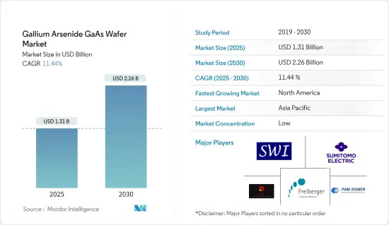
砷化镓 (GaAs) 晶圆市场规模预计在 2025 年为 13.1 亿美元,预计到 2030 年将达到 22.6 亿美元,预测期内(2025-2030 年)的复合年增长率为 11.44%。
GaAs 通常用于电子工业,主要用于半导体製造。 GaAs 晶圆在 LED、雷射二极体、光电元件和单晶微波积体电路等产品中的应用越来越多,被认为是推动研究市场成长的主要因素之一。规范这种化合物的价格将为砷化镓(GaAs)芯片製造商创造成长机会。
砷化镓或GaAs是由两种元素组成的复合材料。用于製造 GaAs 晶片的半导体是一种直接带隙半导体,它允许电子快速穿过组件而不会受到太多干扰,这使得它们特别适用于光电设备。
智慧型手机和运算设备的日益普及以及发光二极体(LED)在通用照明中的日益普及是该市场的主要成长动力。物联网的出现也是推动此市场趋势扩大的重大因素之一。这项技术也创造了采用基于 GaAs 的 IC 的高频通讯设备的需求。
因此,随着多家电信业者扩大其通讯基础设施,对 GaAs 晶圆的需求预计将增加,这将对未来几年研究市场的成长产生积极影响。此外,GaAs晶圆的独特特性使得电子、航太和国防、通讯等各个终端用户产业对GaAs晶圆的需求不断增加,也推动了全球对GaAs晶圆的需求。
例如,GaAs晶片是一种耐辐射损伤的宽直接带隙材料,使其成为高功率空间电子和光学窗口的理想选择,预计将提供市场扩展机会并催生新的市场趋势和使用案例,例如电子战系统、电动飞机和宽频行动电话网路技术的发展。
然而GaAs晶圆的价格是其使用率低的一大缺点。为了解决这些问题,研究人员已经找到了生产低成本砷化镓薄膜的新方法,这有助于生产硅的替代设备,从而支持不断增长的研究市场。
COVID-19 疫情在全球爆发,以及各国政府随后为遏制病毒传播而采取的果断行动,对半导体行业产生了明显影响,影响了半导体元件的生产并降低了客户需求,从而阻碍了全球市场的成长。然而,数位技术的普及大大增加了对先进家用电子电器和支援数位基础设施的需求,从而对研究市场的成长产生了积极影响。
砷化镓(GaAs)晶圆市场趋势
高频电子产品占据市场主导地位
在GaAs基板上製作的射频(RF)装置广泛应用于无线区域网路(WLAN)、4G/5G基地台、行动通讯、卫星通讯、Wi-Fi通讯等无线通讯应用。这些趋势发展代表了支援4G和5G服务的智慧型手机和其他行动装置所需的下一代超小型高效能射频前端晶片组开发的重要里程碑。
此外,GaAs晶圆的效率不断提高、低耗电量,正在鼓励市场参与企业采用它们,这也对GaAs晶圆的需求产生了积极影响。光电子元件以前广泛应用于电脑周边设备和短距离光纤通讯。儘管如此,扩增实境(AR)、光达和脸部辨识等新应用的需求仍然很高。
全球网路普及率不断上升,尤其是印度和巴西等新兴国家,正在刺激对 GaAs 晶圆的需求。此后,对Wi-Fi连接产品到光纤网路、回程传输、基地台和无线通讯基础设施的需求不断增加,支援了网路在世界各地的普及。
此外,行动资料消费率的不断增长和物联网设备的广泛应用也推动了对 Wi-Fi 和其他无线通讯设备的需求。这些产品和无线通讯相关技术的高成长率正在推动GaAs晶圆的采用。例如,根据5G America的预测,全球行动5G用户数将从2023年的190万增加到2027年的590万。
预测期内亚太地区将占据市场主导地位
亚太地区对智慧家用电子电器的需求日益增长。中国、台湾、日本和印度对智慧型手机、穿戴式装置、电脑和笔记型电脑等先进科技设备的需求快速成长,进一步推动了该地区市场的成长。由于 GaAs 产品比基于硅的设备提供更好的资料传输和质量,因此连接性得到改善,因此需求量很大。此外,GaAs产品可以大规模生产,且产量比率率较高,从而促进业务成长。互联网的日益普及、4G 和 5G 网路的扩张以及电子产业也有望推动该地区 GaAs 晶圆市场的发展。
亚太地区的主要驱动因素之一是对计算设备、智慧型手机、平板电脑和笔记型电脑等先进技术设备的需求不断增长。由于晶体管等 GaAs 产品可用于智慧型手机和其他无线通讯设备,不断增长的需求正推动对 GaAs 晶圆的需求以可观的速度成长。
中国是主导电子产业市场的领先国家,这得益于政府的大力支持,促进了中国研究市场的发展。例如,中国政府透过向产业相关人员提供资金来促进国内技术市场的发展。这些趋势正在鼓励新参与企业扩大在该国的业务。例如,2023年2月,GaAs晶圆基板等化合物半导体晶圆基板製造商AXT宣布扩建北京工厂。该公司投资了原材料提取设施,以进一步巩固其作为复合半导体基板领先供应商的地位。
中国也是5G基础设施开发以及其他家用电子电器和电动车解决方案采用的领导者之一。例如,根据工信部的数据,到2022年终,中国将拥有约231万个5G基地台。这些产业的成长为中国研究市场的成长创造了良好的前景。
台湾正见证晶圆市场成为技术发展的重点领域之一。因此,预计台湾也将在全球GaAs晶圆市场占有较大份额。台湾公司正在解决前端和后端先进封装架构的供应链需求,以适应专用材料和工艺,从而影响所研究的整体市场。
砷化镓(GaAs)晶圆产业概况
砷化镓(GaAs)晶片市场竞争激烈,少数公司占据相当大的市场占有率,包括AXT Inc.、工业、Semiconductor Wafer Inc.、Freiberger Compound Materials GmbH和厦门博威新材料。现有企业正致力于透过大量投资研发并向客户提供更好、技术更先进的产品来巩固其地位。
2023 年 5 月,半导体晶圆专家 QE 宣布推出一系列专为 Micro LED 显示器认证而设计的新型 200 毫米 RGB 外延晶圆。据该公司称,GaN和GaAs外延预计将继续在推动微型LED的快速应用方面发挥关键作用。
2022年5月,南加州大学资讯科学研究所的 MOSIS Services 与 WIN Semiconductors, Inc. 签署了谅解备忘录,利用 WIN Semiconductors 的 GaAs 和 GaN 製程技术加速开发 GaAs 和 GaN单晶微波积体电路。该伙伴关係将透过 MOSIS Services 与 WIN Semiconductors 合作的多计划晶圆 (MPW)计划支援可靠、创新和高效的设计和原型製作流程。
其他福利
- Excel 格式的市场预测 (ME) 表
- 3 个月的分析师支持
目录
第 1 章 简介
- 研究假设和市场定义
- 研究范围
第二章调查方法
第三章执行摘要
第四章 市场洞察
- 市场概况
- 产业吸引力-波特五力分析
- 供应商的议价能力
- 买家的议价能力
- 新进入者的威胁
- 替代品的威胁
- 竞争对手之间的竞争
- 技术简介
- 液相封装直拉法 (LEC) 生长 GaAs
- 垂直梯度冻结 (VGF) 生长 GaAs
- COVID-19 市场影响评估
第五章 市场动态
- 市场驱动因素
- 全球 5G 基础设施的采用日益增多
- 光电设备需求激增
- 市场限制
- 製造成本高
第六章 市场细分
- 按应用
- 高频电子元件
- 发光二极体
- 光电设备
- 光子装置
- 其他用途
- 按地区
- 美国
- 台湾
- 中国
- 日本
- 英国
- 德国
- 世界其他地区
第七章 竞争格局
- 公司简介
- Semiconductor Wafer Inc
- AXT Inc.
- Freiberger Compound Materials GmbH
- Xiamen Powerway Advanced Material Co. Ltd.
- Sumitomo Electric Industries Ltd.
- Wafer Technology Ltd.
- MTI Corporation
- Vital Materials Co Limited
- Dowa Electronics Materials Co. Ltd.
- American Elements
第八章投资分析
第九章 市场机会与未来趋势
The Gallium Arsenide GaAs Wafer Market size is estimated at USD 1.31 billion in 2025, and is expected to reach USD 2.26 billion by 2030, at a CAGR of 11.44% during the forecast period (2025-2030).
GaAs is mainly used is common in electronics, such as semiconductor manufacturing. The growing adoption of GaAs wafers in products such as LEDs, laser diodes, optoelectronic devices, and monolithic microwave integrated circuits is considered among the primary factors driving the growth of the studied market. The price of this compound being regulated creates more growth opportunities for gallium arsenide (GaAs) wafers manufacturers.
Gallium Arsenide or GaAs is a compound material made up of two elements. The semiconductor used to manufacture GaAs wafers is a direct bandgap semiconductor, meaning that electrons can pass through components much quicker without much interference, making them particularly useful in optoelectronic devices.
The increasing adoption of smartphones and computing devices and the growing penetration of light-emitting diodes (LEDs) in general lighting are significant growth drivers for this market. The advent of IoT has also been one of the major reasons responsible for the increasing market trend. The technology has also created a demand for high-frequency communication devices with GaAs-based ICs.
As a result, with several telecommunication companies expanding their communication infrastructure, the demand for GaAs wafers will increase, which will positively influence the growth of the studied market in the forthcoming years. Additionally, owing to its inherent features, the need for GaAs wafers across various end-user industries such as electronics, aerospace & defense, and communications is increasing, which, in turn, is also driving the demand for GaAs Wafers globally.
For instance, GaAs wafers are also a great choice for high-power outer space electronics and optical windows due to their wide direct bandgap material that resists radiation damage which is also predicted to offer profitable chances for market expansion and give rise to new market trends and use cases, including their higher adoption in electronic warfare systems, electric aircraft, and developments in broadband cellular network technology.
However, the price of GaAs wafers is among the major disadvantage, which explains its low utilization. To solve such issues, researchers have achieved new methods of manufacturing thin films of low-cost gallium arsenide to help create devices that would replace silicon to support the studied market's growth.
The global outbreak of the COVID-19 pandemic and the subsequent decisive government actions taken to curb the spread of the virus had a notable impact on the semiconductor sector, affecting the manufacture of semiconductor components and lowering customer demand, thereby impeding the global market's growth. However, higher exposure to digital technologies significantly enhanced the demand for advanced consumer electronic devices and supporting digital infrastructure, which positively influenced the growth of the studied market.
Gallium Arsenide (GaAs) Wafer Market Trends
Radio Frequency Electronics to Hold the Significant Share in the Market
Radio-frequency (RF) devices produced with GaAs substrates are widely used in wireless communication applications, including wireless networks (WLAN), 4G/5G base stations, mobile communication, satellite, and Wi-Fi communications. The development of such trends marks an important milestone in developing next-generation, ultra-compact, and high-performance RF front-end chipsets that are needed for smartphones and other handsets, supporting 4G and 5G services.
GaAs wafers' higher efficiency and lower power consumption are also enticing market participants to adopt them, positively influencing the demand for GaAs wafers. Optoelectronic devices were previously widely used in computer peripherals and short-range optical communications. Still, they are in high order for new applications such as augmented reality (AR), lidar, and facial recognition.
Globally, internet penetration is rising, especially in developing countries such as India and Brazil, stimulating the demand for GaAs wafers. Subsequently, the need for fiber-optic networks and backhaul, base stations, and Wi-Fi connectivity products with wireless communication infrastructure and have supported the growing penetration of the internet worldwide, which, in turn, is driving the adoption of GaAs wafers.
Further, the growth of mobile data consumption rate and the wide adoption of IoT devices also propel the requirement for Wi-Fi and other wireless communication devices. As a result of the high growth rates for such products and technologies related to wireless communications are aiding the adoption of GaAs wafers. For instance, according to 5G America, the global number of mobile 5G subscriptions is expected to grow from 1.9 million in 2023 to 5.9 million by 2027.
Asia Pacific to Dominate the Market During the Forecast Period
The Asia Pacific region has an increasing demand for intelligent consumer electronic devices. China, Taiwan, Japan, and India have surging demand for advanced technological devices such as smartphones, wearables, computers, and laptops, further augmenting the regional market's growth. GaAs products offer better connectivity through enhanced data transmission and quality than silicon-based devices, so their demand has increased. Additionally, GaAs products can be manufactured on large scales with high yield rates, which improves business growth. The increasing Internet penetration, expansion of 4G and 5G networks, and the electronic industry are also expected to fuel the development of the GaAs wafer market in the region.
One major driving factor in the Asia Pacific region is the growing demand for advanced technological devices such as computing devices, smartphones, tablets, and laptops. As GaAs products such as transistors can be used for smartphones and other wireless communication devices, the growing demand is driving the need for GaAs wafers at a promising rate.
China is the major country dominating the market for the electronics industry owing to considerable government support, which is fostering the development of the studied market in China. For instance, the Chinese government is promoting its domestic technology market by funding the industry players. Such trends are encouraging new players to expand their presence in the country. For instance, in February 2023, AXT, a manufacturer of compound semiconductor wafer substrates such as GaAs wafer substrates, announced an expansion of operations at its Beijing facility. The company invested in raw material extraction facilities to further strengthen its position as the leading provider of compound semiconductor substrates.
China is also among the leading countries in 5G infrastructure development and adopting other consumer electronic and electric mobility solutions. For instance, according to MIIT, by the end of 2022, China had about 2.31 million 5G base stations. Together the growth of these industries is creating a favorable outlook for the growth of the studied market in China.
Taiwan has witnessed the wafer market as one of the critical areas of technological development. As a result, Taiwan is also expected to hold a significant market share in the global GaAs wafer market. Companies across Taiwan are addressing the supply chain needs of front and back-end advanced wafer-level packaging architectures to cater to specialty materials and processes, thus, influencing the overall market studied.
Gallium Arsenide (GaAs) Wafer Industry Overview
The Gallium Arsenide GaAs Wafer Market is competitive and highly concentrated with a few companies such as AXT Inc, Sumitomo Electric Industries Ltd., Semiconductor Wafer Inc, Freiberger Compound Materials GmbH, Xiamen Powerway Advanced Material Co. Ltd, holding a significant market share. Established companies focus on strengthening their position by investing heavily in R&D and providing customers with better and technologically advanced products.
In May 2023, QE, a semiconductor wafer specialist, introduced a new range of 200mm RGB epitaxial wafer products specifically designed for microLED display qualification. According to the company, GaN and GaAs epitaxy is anticipated to continue to play a crucial role in driving the rapid adoption of microLEDs.
In May 2022, The MOSIS Service of Information Sciences Institute, University of Southern California, and WIN Semiconductors Corp. signed a Memorandum of Understanding (MoU) to accelerate the development of GaAs and GaN monolithic microwave integrated circuits with WIN Semiconductors' GaAs and GaN process technologies. The partnership will support the reliable, innovative, and effective design and prototyping flow through the multi-project wafer (MPW) projects with the MOSIS Service and WIN Semiconductors.
Additional Benefits:
- The market estimate (ME) sheet in Excel format
- 3 months of analyst support
TABLE OF CONTENTS
1 INTRODUCTION
- 1.1 Study Assumptions and Market Definition
- 1.2 Scope of the Study
2 RESEARCH METHODOLOGY
3 EXECUTIVE SUMMARY
4 MARKET INSIGHTS
- 4.1 Market Overview
- 4.2 Industry Attractiveness - Porter's Five Forces Analysis
- 4.2.1 Bargaining Power of Suppliers
- 4.2.2 Bargaining Power of Buyers
- 4.2.3 Threat of New Entrants
- 4.2.4 Threat of Substitute Products
- 4.2.5 Intensity of Competitive Rivalry
- 4.3 Technology Snapshot
- 4.3.1 Liquid Encapsulated Czochralski (LEC) Grown GaAs
- 4.3.2 Vertical Gradient Freeze (VGF) Grown GaAs
- 4.4 Assessment of the Impact of COVID-19 on the Market
5 MARKET DYNAMICS
- 5.1 Market Drivers
- 5.1.1 Increasing Adoption of 5G Infrastructure Across the World
- 5.1.2 Surging Demand for Opto-electronic Devices
- 5.2 Market Restraints
- 5.2.1 High Production Cost
6 MARKET SEGMENTATION
- 6.1 By Application
- 6.1.1 Radio Frequency Electronics
- 6.1.2 Light Emitting Diodes
- 6.1.3 Photovoltaic Devices
- 6.1.4 Phototonic Devices
- 6.1.5 Other Applications
- 6.2 By Geography
- 6.2.1 United States
- 6.2.2 Taiwan
- 6.2.3 China
- 6.2.4 Japan
- 6.2.5 United Kingdom
- 6.2.6 Germany
- 6.2.7 Rest of the World
7 COMPETITIVE LANDSCAPE
- 7.1 Company Profiles
- 7.1.1 Semiconductor Wafer Inc
- 7.1.2 AXT Inc.
- 7.1.3 Freiberger Compound Materials GmbH
- 7.1.4 Xiamen Powerway Advanced Material Co. Ltd.
- 7.1.5 Sumitomo Electric Industries Ltd.
- 7.1.6 Wafer Technology Ltd.
- 7.1.7 MTI Corporation
- 7.1.8 Vital Materials Co Limited
- 7.1.9 Dowa Electronics Materials Co. Ltd.
- 7.1.10 American Elements
8 INVESTMENT ANALYSIS
9 MARKET OPPORTUNITIES AND FUTURE TRENDS
 砷化镓晶片市场:2026-2032年全球市场预测(按掺杂、直径、晶片类型、应用和销售管道划分)光学热测量系统市场:依产品类型、技术、应用、最终用户和销售管道,全球预测,2026-2032年全球α-氧化铝市场(依产品类型、粒径、终端用途产业及通路划分)预测(2026-2032年)
 全球砷化镓晶片市场规模、份额、趋势和成长分析报告(2026-2034年)晶圆清洗设备市场:2026-2032年全球预测(按设备类型、晶圆尺寸、基板材料、应用和最终用户划分)晶圆载体清洗机市场按自动化程度、技术、清洗介质、纯度、应用和最终用户划分-2026-2032年全球预测
 GaAS晶圆市场-全球产业规模、份额、趋势、机会及预测,依产品类型(LEC生长GaAS、VGF生长GaAS及其他)、产品应用(射频、LED、VCSEL、光伏)、地区及竞争格局划分,2020-2030年预测磷化铟晶片市场-2025-2030年预测半导体晶圆分选系统市场(依设备类型、分选技术、类别和最终用户)-2025-2030 年全球预测
 晶圆温度测量系统的全球市场