


 |
市场调查报告书
商品编码
1687834
磷化铟晶片-市场占有率分析、产业趋势与统计、成长预测(2025-2030)Indium Phosphide Wafer - Market Share Analysis, Industry Trends & Statistics, Growth Forecasts (2025 - 2030) |
||||||
※ 本网页内容可能与最新版本有所差异。详细情况请与我们联繫。
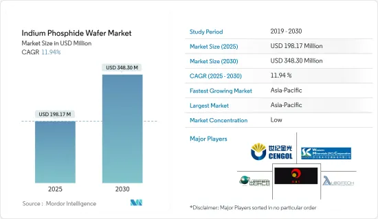
预计 2025 年磷化铟晶片市场规模为 1.9817 亿美元,到 2030 年将达到 3.483 亿美元,预测期内(2025-2030 年)的复合年增长率为 11.94%。
磷化铟 (InP) 具有可用于生产高效雷射、调变和灵敏检测器的特性。它还可以产生雷射讯号并将该讯号转换为电子形式以供识别。这些用于企业网路和资料中心、远距光纤连接、3G、5G 和 LTE基地台的无线连接以及卫星通讯。这些日益增长的需求正在推动市场的发展。
主要亮点
- 磷化铟晶片越来越多地被用于汽车雷射雷达、3D感测、消费穿戴设备和通讯领域的资料通讯的成长。预计这将在预测期内推动市场发展。 InPinc 的主要应用还包括 5G通讯、使用光和雷射的资料中心连接、光纤雷射和检测器、军事和 5G通讯通讯使用的硅光电、射频放大器和开关以及健康领域的红外线热感成像。
- 被称为光电装置的电子元件可以侦测和调节光。光电设备将电资讯转换为红外线或可见光能量,反之亦然。光电子技术应用于太阳能发电、光纤通讯系统、监视器和控制电路以及电眼。光电元件用于量子连锁雷射和受激发射的注入雷射二极体。 LED 和影像感测器用于数位成像系统、包装和安全应用。
- 根据 2020 年 11 月发布的爱立信移动报告,到 2020 年底,全球行动资料流程量预计将达到每月约 51 EB(Exabyte)。预计到 2026 年,这一数字将成长近 4.5 倍,达到每月 226 EB。这一数字意味着超过 60 亿人使用智慧型手机、笔记型电脑和一系列新设备同时消耗行动资料。
- 半导体硅片是电子工业的基础,也是许多微电子设备的关键零件。随着当前技术、电子设备移动化和数数位化的进步,这些物品现在被广泛应用于各种设备。此外,对更小设备的需求大大增加了对单一设备附加功能的需求,从而推高了硅晶片的价格。
- 新冠疫情导致全球大部分地区实施封锁,半导体设备产业多种产品的生产陷入停滞。封锁措施减少了对家用电子电器的需求,影响了全球半导体产业。全球汽车需求和出口出货量的持续下降对半导体市场产生了负面影响,目前正在减缓半导体製造设备的需求。
磷化铟晶片市场趋势
消费性电子产品是市场领导者
- 穿戴式科技是一种发展趋势,它将电子产品融入日常活动,并能够佩戴在身体的任何部位,以适应不断变化的生活方式。诸如连接到互联网以及提供网路和设备之间资料交换选项等趋势正在引领可穿戴技术的发展趋势。
- 根据Cisco预测,全球连网穿戴装置的数量每三年就会翻一番,从2016年的3.25亿台成长到2019年的7.22亿台,预计到2022年将超过10亿台。
- 此外,根据日本内务部的数据,截至 2021 年,超过 7% 的日本家庭拥有穿戴式装置。在整个研究期间(2014-2021年),穿戴式装置的家庭普及率稳定上升,从2014年的0.5%上升到2020年的5%。
- 全球都市化的不断上升推动了对先进、美观的产品的需求,这些产品能够满足消费者的需求,例如单一设备中的多种功能和时间表。此外,全球千禧世代是智慧型手錶的早期采用者,因为他们能够更好地追踪正常工作时间和奢侈标准消费。
- 例如,根据爱立信的数据,全球智慧型手机用户数从2020年的59.24亿激增至2021年的62.59亿。预计2027年将达到76.9亿部。
- 此外,根据诺基亚2022年年度行动宽频指数报告,不断扩大的4G设备生态系统正在推动4G用户和资料消费的成长。 2021年,印度智慧型手机出货量创历史新高,超过1.6亿部,其中包括3000万部5G设备,其中超过80%的活跃设备支援4G,超过1000万部活跃的5G设备支援5G。此外,诺基亚的一份报告预测,到 2025 年,智慧型手机普及率将达到 60-75%。
亚太地区可望成为成长最快的市场
- 亚太地区在全球半导体代工市场占有较大份额,拥有台积电、三星电子等巨头。台湾、韩国、日本和中国在该地区也占有很大份额。根据半导体产业美国(SIA)的数据,从1990年到2020年,美国在全球晶圆厂装置容量中的份额一直在稳步下降。同一时期,亚洲新的半导体工厂快速发展,目前已占全球产能的相当大一部分。
- 中国有着非常雄心勃勃的半导体计画。在1500亿美元基金的支持下,中国计划发展国内积体电路产业并生产更多晶片。大中华区(包括中国香港和台湾)是一个地缘政治热点。美国贸易战进一步加剧了该地区的紧张局势,该地区集中了关键工艺技术,迫使许多中国公司投资半导体代工厂。
- 中国于2021年3月发布的2021-2025年新五年规划将加强基础研究作为重要优先事项。预计2021年中央政府对基础研究的支出将成长11%,远高于计画的整体研发投入7%和6%的GDP成长目标。半导体被认定为七个优先提供资金和资源的领域之一。设计公司开发奈米级积体电路,执行电子设备运作的关键任务,包括运算、储存、网路连接和电源管理。由于晶片需求强劲,预计 2021 年利润将成长一倍以上。中国领先的半导体代工厂已为 2022 年的产能开发预留了创纪录的资金。今年,中芯国际已预留了 50 亿美元的资本支出,高于 2021 年的 45 亿美元。
- 中国在7nm晶片生产方面距离自力更生越来越近。据报道,中国在 7nm 晶片製造流程方面取得了突破,并在製造过程的多个环节开发了工具和技术,以减少对海外设备和材料供应商的依赖。
- 研究和合作的大幅扩展将进一步提高市场成长率。例如,LioniX International (LXI) 和中国科学院微电子研究所 (IMECAS) 已同意透过积极支援能力和提供两个平台来扩大其光子积体电路 (PIC) 平台伙伴关係。 PIC 的重要平台包括 SOI(绝缘体上硅)、InP(磷化铟)和基于氮化硅的 TriPleX 平台。这些平台可透过多计划晶圆(MPW)存取取得。
磷化铟晶片产业概况
磷化铟晶片製造领域正在见证领先製造商的不断增加,预计在预测期内竞争对手之间的竞争将更加激烈。 JX Nippon Mining & Metals 和 Powerway Advanced Materials 等市场现有企业对整个市场产生了相当大的影响。
- 2022 年 3 月:英特尔透露在德国建造第二家晶片製造地(即「大型工厂」)的计画。此外,2021 年 8 月,ACM Research Inc. 推出了其 Bevel Etch 产品,进一步扩展了 ACM 的综合湿式工具产品线。该工具最大限度地减少了边缘污染对后续製程步骤的影响,并提高了晶片製造的产量比率。
- 2022 年 2 月:加拿大政府宣布对加拿大半导体和光电产业进行重大投资。这项 2.4 亿加元的投资将巩固加拿大在光电的全球领先地位,并加强半导体开发和製造。加拿大拥有100多家从事微晶片研发的国内外半导体公司。在化合物半导体、电子机械系统(MEMS)和先进封装等领域拥有 30 多个应用实验室和 5 个商业设施。
其他福利:
- Excel 格式的市场预测 (ME) 表
- 3个月的分析师支持
目录
第一章 引言
- 研究假设和市场定义
- 研究范围
第二章调查方法
第三章执行摘要
第四章 市场洞察
- 市场概览
- 产业吸引力-波特五力分析
- 供应商的议价能力
- 买家/消费者的议价能力
- 新进入者的威胁
- 替代品的威胁
- 竞争对手之间的竞争
- 产业价值链分析
- 技术简介
- COVID-19 产业影响评估
第五章市场动态
- 市场驱动因素
- 光电设备的使用日益增多
- 资料通讯业务与5G的发展
- 市场限制
- 与其他替代品的竞争
第六章市场区隔
- 依直径
- 50.8 毫米或 2 英寸
- 76.2毫米或3英寸
- 超过 100 毫米或 4 英寸
- 最终用户产业应用
- 消费性电子产品
- 通讯设备
- 医疗保健
- 其他最终用户产业
- 按地区
- 北美洲
- 欧洲
- 亚太地区
- 世界其他地区
第七章竞争格局
- 公司简介
- AXT Inc.
- Wafer World Inc.
- Logitech Ltd.
- Western Minmetals(SC)Corporation
- Century Goldray Semiconductor Co. Ltd
- Semiconductor Wafer Inc.
- Ding Ten Industrial Inc.
- Sumitomo Electric Semiconductor Materials Inc.(Sumitomo Electric Industries Ltd)
- Xiamen Powerway Advanced Material Co. Ltd
- JX Nippon Mining & Metals Corporation(Eneos Holdings Inc.)
第八章投资分析
第九章 市场机会与未来趋势
The Indium Phosphide Wafer Market size is estimated at USD 198.17 million in 2025, and is expected to reach USD 348.30 million by 2030, at a CAGR of 11.94% during the forecast period (2025-2030).
Indium phosphide (InP) has properties that produce highly efficient lasers, modulators, and sensitive photodetectors. It can also generate laser signals and convert and identify those signals back to the electronic form. These are used for company networks and data centers, long-haul optical fiber connections over far distances, wireless connections for 3G, 5G, and LTE base stations, and satellite communication. The growth in such requirements is driving the market.
Key Highlights
- Indium phosphide wafers are increasingly adopted in the manufacture of LiDAR for automotive, 3D sensing, consumer wearables, and the growth in datacom in the telecommunication sector. This is expected to drive the market during the forecast period. In addition, some of the major applications of InPinclude 5G communications, data center connectivity that uses lights and lasers, fiber optic lasers and detectors, silicon photonics, RF amplifiers, and switches used in military and 5G communications, and infrared thermal imaging in health.
- Electronic components known as optoelectronic devices detect and regulate light. They convert electrical information into infrared or visible energy and vice versa. It is utilized in photovoltaic power supply, optical fiber communication systems, monitor and control circuits, and electric eyes. Optoelectronic components are used in quantum cascade lasers and injection laser diodes for stimulated emission. LEDs and image sensors are utilized in digital imaging systems, packaging, and safety applications.
- According to the Ericsson Mobility Report published in November 2020, the global mobile data traffic was estimated to reach around 51 EB (exabytes) per month by the end of 2020. This was projected to grow by a factor of almost 4.5 to reach 226 EB per month in 2026. This figure represents the mobile data that will be consumed by greater than 6 billion people using smartphones, laptops, and a multitude of new devices at a time.
- The semiconductor silicon wafer serves as the foundation of the electronics industry and is the main component of many microelectronic devices. With the current advances in the technology landscape, electronic mobility, and digitalization, these items are finding use in a wide range of devices. The requirement for additional capability from a single device has also grown dramatically as a result of the need for small-sized gadgets, which boosts the price of the silicon wafer.
- The COVID-19 pandemic has halted the manufacturing of several items in the semiconductor production equipment industry owing to the continued lockdown in most regions across the world. Lockdown measures reduced the demand for consumer electronic gadgets, which had a global impact on the semiconductor sector. The continued decline in worldwide demand and export shipments for automobiles caused a negative impact on the semiconductor market, which is currently slowing down the demand for semiconductor manufacturing equipment.
Indium Phosphide Wafer Market Trends
Consumer Electronics Segment Expected to Drive the Market
- Wearable technology, a developing trend, integrates electronics into daily activities and addresses the changing lifestyles with the ability to be worn on any part of the body. Factors such as the ability to connect to the internet and provide data exchange options between a network and a device are leading to the trend of wearable technology.
- According to Cisco Systems, the number of connected wearable devices globally has doubled in the span of three years, increasing from 325 million in 2016 to 722 million in 2019. The number of devices is forecasted to be over 1 billion by 2022.
- Further, according to the Ministry of Internal Affairs and Communications (Japan), as of 2021, over 7% of households in Japan owned a wearable device. The household penetration rate of wearable devices steadily increased throughout the surveyed period (2014-2021), rising from 0.5% in 2014 to 5% in 2020.
- The rising rates of urbanization in various parts of the world have driven the demand for advanced, aesthetically appealing products that possess the ability to serve the consumers' requirements better, such as multiple features in one device and time schedules. Moreover, the vast millennial population across the globe has been quick to adopt smartwatches, owing to the increased spending ability on their regular work hours tracking and luxury standards.
- For instance, according to Ericsson, the number of smartphone subscriptions worldwide witnessed an upsurge from 5,924 million in 2020 to 6,259 million in 2021. The number is estimated to reach 7,690 million in 2027.
- Further, according to the Nokia annual mobile broadband index report 2022, the growing ecosystem of 4G-capable devices is driving the growth in 4G subscribers and data consumption. India recorded the highest-ever shipment of over 160 million smartphones, including 30 million 5G devices, in 2021, with active 4G capable devices crossing 80% and the number of active 5G capable devices crossing 10 million. The Nokia report also forecasted that user adoption will increase to 60-75% of the smartphone user base by 2025.
Asia-Pacific Expected to be the Fastest-growing Market
- The Asia-Pacific region commands a prominent share of semiconductor foundries globally, with major companies such as TSMC and Samsung Electronics. Taiwan, South Korea, Japan, and China have a significant market share in the region. According to the US Semiconductor Industry Association (SIA), the US share of the global installed wafer fab capacity constantly declined from 1990 to 2020. During the same period, Asia saw a meteoric rise in developing new fabs to the point where it now accounts for a significant share of the world's capacity.
- China has a very ambitious semiconductor agenda. Backed by USD 150 billion in funding, the country is developing its domestic IC industry and plans to make more of its chips. Greater China, which encompasses Hong Kong, China, and Taiwan, is a geopolitical hotspot. The US-China trade war is compounding tensions in an area where all the leading process technology is located, forcing many Chinese companies to invest in their semiconductor foundries.
- China's new five-year plan for 2021-2025, announced in March 2021, established that boosting basic research was a critical priority. The central government's spending on basic research was expected to increase by 11% in 2021, well above the 7% planned for the overall R&D investment and the 6% target for GDP growth. Semiconductors were designated as one of the seven areas that will be given priority in terms of funding and resources. Firms involved in design develop nanometer-scale integrated circuits that perform the critical tasks that make electronic devices work, such as computing, storage, network connectivity, and power management. The profit was estimated to more than double in 2021 because of the robust chip demand. China's leading semiconductor foundry set aside a record sum for capacity development in 2022. This year, Semiconductor Manufacturing International Corp (SMIC) set aside USD 5 billion for capital spending, up from USD 4.5 billion in 2021.
- China is moving significantly closer to self-reliance in 7 nm chip production. China has made breakthroughs in its 7 nm chip-making process, reportedly developing tools and know-hows for several segments of the manufacturing process amid efforts to reduce reliance on foreign equipment and material vendors.
- The significant research and partnership growth further bolsters the market growth rate. For instance, LioniXInternational (LXI) and the Institute of Microelectronics Chinese Academy of Science (IMECAS) agreed to expand their Photonic Integrated Circuit (PIC) platform partnership by actively supporting the functionality and offering both platforms. The critical platforms in the PIC landscape include Silicon On Insulator (SOI), Indium Phosphide (InP), and the silicon nitride-based TriPleXplatform. These platforms are available through Multi-Project Wafer (MPW) access.
Indium Phosphide Wafer Industry Overview
The growing presence of large manufacturers in the indium phosphide wafer manufacturing sector is expected to intensify competitive rivalry during the forecast period. Market incumbents, such as JX Nippon Mining & Metals Corporation and Powerway Advanced Material Co. Ltd, considerably influence the overall market.
- March 2022: Intel revealed plans for a second new 'Megafab," a chipmaking site in Germany, with an expected USD 88 billion in investments across several European countries. Further, in August 2021, ACM Research Inc. launched its Bevel Etch product, which further expanded ACM's comprehensive offering of wet tools. This tool minimizes the impact of edge contamination for subsequent process steps and improves chip manufacturing yield.
- February 2022: The Government of Canada announced a significant investment in the Canadian semiconductor and photonics industries. The investment of CAD 240 million will help solidify Canada's role as a global leader in photonics and will bolster the development and manufacturing of semiconductors. Over 100 domestic and international semiconductor companies work on microchip research and development in Canada. There are over 30 applied research laboratories and five commercial facilities for areas including compound semiconductors, microelectromechanical systems (MEMS), and advanced packaging.
Additional Benefits:
- The market estimate (ME) sheet in Excel format
- 3 months of analyst support
TABLE OF CONTENTS
1 INTRODUCTION
- 1.1 Study Assumptions and Market Definition
- 1.2 Scope of the Study
2 RESEARCH METHODOLOGY
3 EXECUTIVE SUMMARY
4 MARKET INSIGHTS
- 4.1 Market Overview
- 4.2 Industry Attractiveness - Porter's Five Forces Analysis
- 4.2.1 Bargaining Power of Suppliers
- 4.2.2 Bargaining Power of Buyers/Consumers
- 4.2.3 Threat of New Entrants
- 4.2.4 Threat of Substitute Products
- 4.2.5 Intensity of Competitive Rivalry
- 4.3 Industry Value Chain Analysis
- 4.4 Technology Snapshot
- 4.5 Assessment of the Impact of COVID-19 on the Industry
5 MARKET DYNAMICS
- 5.1 Market Drivers
- 5.1.1 Increasing Use of Optoelectronic Devices
- 5.1.2 Growth of Datacom Business and 5G
- 5.2 Market Restraints
- 5.2.1 Competition from Other Substitutes
6 MARKET SEGMENTATION
- 6.1 By Diameter
- 6.1.1 50.8 mm or 2 "
- 6.1.2 76.2 mm or 3 "
- 6.1.3 100 mm or 4" and Above
- 6.2 By End-user Industry Application
- 6.2.1 Consumer Electronics
- 6.2.2 Telecommunications
- 6.2.3 Medical
- 6.2.4 Other End-user Industry Applications
- 6.3 By Geography
- 6.3.1 North America
- 6.3.2 Europe
- 6.3.3 Asia-Pacific
- 6.3.4 Rest of the world
7 COMPETITIVE LANDSCAPE
- 7.1 Company Profiles
- 7.1.1 AXT Inc.
- 7.1.2 Wafer World Inc.
- 7.1.3 Logitech Ltd.
- 7.1.4 Western Minmetals (SC) Corporation
- 7.1.5 Century Goldray Semiconductor Co. Ltd
- 7.1.6 Semiconductor Wafer Inc.
- 7.1.7 Ding Ten Industrial Inc.
- 7.1.8 Sumitomo Electric Semiconductor Materials Inc. (Sumitomo Electric Industries Ltd)
- 7.1.9 Xiamen Powerway Advanced Material Co. Ltd
- 7.1.10 JX Nippon Mining & Metals Corporation (Eneos Holdings Inc.)
8 INVESTMENT ANALYSIS
9 MARKET OPPORTUNITIES AND FUTURE TRENDS
 全球α-氧化铝市场(依产品类型、粒径、终端用途产业及通路划分)预测(2026-2032年)
 全球砷化镓晶片市场规模、份额、趋势和成长分析报告(2026-2034年)晶圆清洗设备市场:2026-2032年全球预测(按设备类型、晶圆尺寸、基板材料、应用和最终用户划分)晶圆载体清洗机市场按自动化程度、技术、清洗介质、纯度、应用和最终用户划分-2026-2032年全球预测
 GaAS晶圆市场-全球产业规模、份额、趋势、机会及预测,依产品类型(LEC生长GaAS、VGF生长GaAS及其他)、产品应用(射频、LED、VCSEL、光伏)、地区及竞争格局划分,2020-2030年预测磷化铟晶片市场-2025-2030年预测半导体晶圆分选系统市场(依设备类型、分选技术、类别和最终用户)-2025-2030 年全球预测
 晶圆温度测量系统的全球市场全球磷化铟晶片市场规模(按类型、应用、区域范围和预测)抛光硅片市场:未来预测(2025-2030)