


 |
市场调查报告书
商品编码
1687765
半导体蚀刻设备:市场占有率分析、行业趋势和统计、成长预测(2025-2030 年)Semiconductor Etch Equipment - Market Share Analysis, Industry Trends & Statistics, Growth Forecasts (2025 - 2030) |
||||||
※ 本网页内容可能与最新版本有所差异。详细情况请与我们联繫。
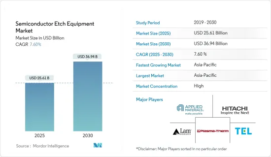
预计半导体蚀刻设备市场规模在 2025 年将达到 256.1 亿美元,在 2030 年将达到 369.4 亿美元,预测期内(2025-2030 年)的复合年增长率为 7.6%。
主要亮点
- 资本投资推动半导体蚀刻设备的成长:由于半导体加工的资本投资增加,半导体蚀刻设备市场正在经历强劲成长。全球对半导体产业的投资正在激增,其中法国投资19亿美元,德国投资120亿美元用于微电子计划。美国公司占据市场主导地位,控制主要製造製程设备类别的50%以上,而日本则占了光阻剂加工市场的90%。投资激增推动了对生产更小、更薄、更快的设备至关重要的先进蚀刻技术的需求。
- 中国投资:中国宣布计划在 2020 年至 2025 年期间投资 1.4 兆美元,重点投资包括半导体在内的先进技术。
- 在日本联合投资:台积电和索尼公司共同投资70亿美元在日本新建晶片工厂。
- 欧盟重点关注数位基础设施:欧盟已将其 9,170 亿美元新冠疫情復苏基金中的 20% 分配给数位基础设施,重点是微电子技术。
- 英特尔的巨额投资:英特尔宣布计划在欧洲投资 880 亿美元,包括在德国建立一个新的大型晶圆厂。
- 技术进步重塑市场格局:快速的技术进步正在重塑半导体蚀刻设备市场,明显转向消费量更少化学品且更适合自动化晶圆厂製造的电浆蚀刻系统。这种演变是由对更节能和更高性能电子设备日益增长的需求所驱动,从而刺激了小型化半导体积体电路 (IC) 的发展。
- 选择性蚀刻:2022 年 2 月,Lam Research 宣布推出一款选择性蚀刻设备,该设备采用创新的晶圆製造技术,用于全栅 (GAA) 电晶体架构。
- 表面处理技术:ClassOne Technology 于 2022 年 7 月在其 Solstice 自动化单晶圆平台中扩展了表面处理 (SP) 技术。
- 热处理创新:Plasma-Therm 凭藉其 Heatpulse 快速热处理 (RTP) 平台进行创新,赢得了全球晶片製造商的多项采购。
- FPD设备开发:我们正在开发能够处理电视、智慧型手机和其他设备的高解析度和低耗电量的FPD製造设备。
- 反映多种应用的市场细分:半导体蚀刻设备市场根据产品类型、蚀刻膜类型和应用进行细分。高密度蚀刻设备引领市场,预计到 2027 年营收将达到 192.8961 亿美元。预计导体蚀刻部分在 2022 年至 2027 年期间的复合年增长率为 4.55%,到预测期结束时将达到 125.5446 亿美元。
- 关键驱动因素:铸造、MEMS、感测器和电力设备是推动市场成长的主要应用领域。
- 智慧型设备和物联网:物联网的采用和对智慧设备日益增长的需求正在推动半导体小型化的需求,从而刺激蚀刻设备市场的发展。
- 太阳能电池湿蚀刻:湿蚀刻因其高选择性和材料保存特性,在太阳能电池製造中不断被应用。
- 投资分析凸显市场潜力:半导体蚀刻设备市场正在进行大量投资,反映了其成长潜力。各公司正在扩大製造能力并加强研发力度,以满足对先进半导体技术日益增长的需求。
- Lam Research 扩张:Lam Research 于 2021 年 8 月在马来西亚开设了最大的工厂,加强了其全球製造地。
- 美国半导体投资:美国政府核准对半导体产业投资500亿美元,重点投资生产、研究和设计。
- 印度的半导体推动:印度已决定在半导体製造业投资 100 亿美元,并计划建立各种製造工厂。
- MIT.nano 扩大研发:2021 年 7 月,MIT.nano 收购了新的 SAMCO感应耦合电浆(ICP) 反应离子刻蚀 (RIE) 工具,以加强对新材料的研究。
半导体蚀刻设备市场趋势
高密度蚀刻设备领域占主要市场占有率
- 主导市场占有率和强劲成长:高密度蚀刻设备领域占最大的市场占有率,占2021年半导体蚀刻设备市场的63.59%,达到125.441亿美元。预计到 2027 年,该领域规模将成长至 192.896 亿美元,复合年增长率为 5.66%。
- 科技进步推动需求:随着各行各业推动万物智慧化,对更小、更有效率设备的需求正在激增。这一趋势正在推动半导体製造技术在高温化学过程中实现精确度,而清洁度和精确的化学剂量是关键。
- 转向先进的蚀刻技术:该行业正在从传统的湿蚀刻转向更高效、更适合单晶圆自动化的等电浆蚀刻系统。这种转变对于开发为更节能的设备供电的紧凑型半导体积体电路至关重要。
- 研发投入:在半导体领域,大量的研发投入至关重要。例如,美国承诺将对半导体相关领域的研究投入增加一倍,旨在推动人工智慧、量子运算和先进无线技术等领域的创新。
产业创新
- ClassOne 的 Solstice 扩充:2022 年 7 月,ClassOne Technology 将新的表面处理技术融入其 Solstice 平台。
- Plasma-Therm 的 RTP 平台:经过最近的全面改革,Plasma-Therm 的旗舰产品 Heatpulse RTP 平台已被多家全球领先的晶片製造商收购。
亚太地区成长强劲
- 市场领导地位与快速成长:2021 年亚太地区占半导体蚀刻设备市场的 84.72%,价值 167.1 亿美元。预计该地区的复合年增长率为 4.52%,到 2029 年达到 238 亿美元。
- 中国力争自力更生:中国在 7nm 晶片生产方面取得了长足进步,在多个半导体製造领域开发了工具和技术。这种自给自足的动力是该地区半导体蚀刻设备投资和创新的主要驱动力。
- 策略投资和合作伙伴关係:该地区吸引了国内外参与者的大量投资。例如,台积电宣布投资28亿美元,以提高在中国的汽车晶片产量。同样,印度也在蓬勃发展,ISMC 计划投资 30 亿美元建造一座半导体製造工厂。
- 在地化製造:全球公司越来越多地在亚太地区进行在地化生产。 2022年2月,Lam Research开始在韩国生产下一代核心设备,加强了与三星电子在记忆体和系统半导体製造的合作。
- 汽车产业推动需求:全自动驾驶汽车的发展预计将对半导体产业产生重大影响,尤其是在亚太地区。随着汽车和半导体行业致力于增强自动驾驶技术,预计对半导体蚀刻设备的需求将激增。
半导体蚀刻设备产业概况
全球领导者主导整合市场:半导体蚀刻设备市场高度整合,由全球参与者和专业公司组成。资本和技术专长方面的高进入门槛意味着最大的参与者占据相当大的市场占有率。该市场主要由拥有强大研究能力的跨国公司推动。
创新和技术力决定市场领导者:主要的市场领先公司有应用材料公司、Lam Research、东京电子有限公司、日立高新技术美国公司等。这些公司致力于等电浆蚀刻系统和高密度感应耦合电浆(ICP)蚀刻技术的开发,并透过不断的研发保持其地位。我们的全球扩张和与主要半导体製造商的策略伙伴关係进一步巩固了我们的市场地位。
未来市场成功的策略:为了占领更大的市场占有率,市场需要专注于精度和效率的创新,特别是对于较小的节点尺寸。扩大製造能力并与研究机构和半导体製造商建立策略伙伴关係也将是关键。此外,满足物联网和人工智慧等趋势推动的半导体日益增长的需求对于在竞争激烈的市场中取得成功也至关重要。
其他福利
- Excel 格式的市场预测 (ME) 表
- 3个月的分析师支持
目录
第一章 引言
- 研究假设和市场定义
- 研究范围
第二章调查方法
第三章执行摘要
第四章 市场洞察
- 市场概览
- 产业吸引力-波特五力分析
- 供应商的议价能力
- 买家的议价能力
- 新进入者的威胁
- 替代品的威胁
- 竞争对手之间的竞争强度
- COVID-19 市场影响评估
第五章市场动态
- 市场驱动因素
- 增加对半导体製程的资本投资
- 快速的技术进步与转型
- 市场限制
- 贸易问题和半导体记忆体市场
第六章市场区隔
- 依产品类型
- 高密度蚀刻设备
- 低密度蚀刻设备
- 蚀刻膜类型
- 导体蚀刻
- 介电蚀刻
- 多晶硅蚀刻
- 按应用
- 铸件
- MEMS
- 感应器
- 功率元件
- 按地区
- 北美洲
- 欧洲
- 亚洲
- 澳洲和纽西兰
- 拉丁美洲
- 中东和非洲
第七章竞争格局
- 公司简介
- Applied Materials Inc.
- Hitachi High Technologies America, Inc.
- Lam Research Corporation
- Tokyo Electron Limited
- Plasma-Therm LLC
- Panasonic Corporation
- SPTS Technologies Limited(Orbotech)
- Suzhou Delphi Laser Co., Ltd
- ULVAC Inc.
第八章投资分析
第九章 市场机会与未来趋势
The Semiconductor Etch Equipment Market size is estimated at USD 25.61 billion in 2025, and is expected to reach USD 36.94 billion by 2030, at a CAGR of 7.6% during the forecast period (2025-2030).
Key Highlights
- Capital Spending Drives Semiconductor Etch Equipment Growth: The Semiconductor Etch Equipment Market is experiencing robust growth, fueled by increased capital spending on semiconductor processing. Global investments in the semiconductor industry have surged, with countries like France allocating USD 1.9 billion and Germany investing USD 12 billion into microelectronics projects. US firms dominate the market, controlling over 50% of major manufacturing process equipment categories, while Japan commands 90% of the photoresist processing market. This investment surge is propelling demand for advanced etching technologies, critical for producing smaller, thinner, and faster devices.
- China's Investment: China announced plans to invest USD 1.4 trillion between 2020 and 2025, focusing on advanced technologies, including semiconductors.
- Joint Investment in Japan: TSMC and Sony Corp. jointly invested USD 7 billion in a new chip factory in Japan.
- EU's Digital Infrastructure Focus: The European Union allocated up to 20% of its USD 917 billion Covid recovery fund toward digital infrastructure, focusing on microelectronics.
- Intel's Mega Investment: Intel unveiled plans for a USD 88 billion investment across Europe, including a new "megafab" in Germany.
- Technological Advancements Reshape Market Landscape: Rapid technological advancements are reshaping the Semiconductor Etch Equipment Market, with a clear shift towards plasma etch systems, which consume fewer chemicals and are more suited for automating single wafer manufacturing. This evolution is driven by the growing demand for energy-efficient electronic devices with improved performance, spurring the development of miniature semiconductor integrated circuits (ICs).
- Selective Etching: Lam Research introduced selective etch devices in February 2022, employing innovative wafer fabrication techniques for gate-all-around (GAA) transistor architectures.
- Surface Preparation Tech: ClassOne Technology expanded its Solstice automated single-wafer platform with surface preparation (SP) technologies in July 2022.
- Thermal Processing Innovation: Plasma-Therm revamped its Heatpulse Rapid Thermal Processing (RTP) platform, securing multiple purchases from global chipmakers.
- FPD Equipment Development: Tokyo Electron continues to evolve its FPD production equipment, optimizing it for higher resolutions and ultra-low power consumption for TVs, smartphones, and other devices.
- Market Segmentation Reflects Diverse Applications: The Semiconductor Etch Equipment Market is segmented by product type, etching film type, and application. High-density etch equipment leads the market, with revenue expected to reach USD 19,289.61 million by 2027. The conductor etching segment is forecasted to grow at a CAGR of 4.55% from 2022 to 2027, reaching USD 12,554.46 million by the end of the forecast period.
- Key Growth Drivers: Foundries, MEMS, sensors, and power devices are key application areas driving market growth.
- Smart Devices and IoT: The adoption of IoT and growing demand for smart devices are increasing the need for miniature semiconductors, fueling the etch equipment market.
- Wet Etching for Solar Cells: Wet etching continues to find applications in solar cell manufacturing due to its high selectivity and material preservation properties.
- Investment Analysis Reveals Market Potential: Significant investments are pouring into the Semiconductor Etch Equipment Market, reflecting its potential for growth. Companies are scaling up manufacturing capacities and boosting R&D efforts to meet the rising demand for advanced semiconductor technologies.
- Lam Research's Expansion: Lam Research Corporation opened its largest facility in Malaysia in August 2021, enhancing its global manufacturing footprint.
- US Semiconductor Investment: The US government approved a USD 50 billion investment in the semiconductor industry, focusing on production, research, and design.
- India's Semiconductor Push: India greenlit a USD 10 billion investment in semiconductor manufacturing, aiming to establish a variety of fabrication plants.
- MIT.nano's R&D Expansion: MIT.nano acquired a new SAMCO inductively coupled plasma (ICP) reactive-ion etching (RIE) system in July 2021, boosting research into novel materials.
Semiconductor Etch Equipment Market Trends
High-Density Etch Equipment Segment Holds Significant Market Share
- Dominant Market Share and Robust Growth: The high-density etch equipment segment holds the largest market share, comprising 63.59% of the semiconductor etch equipment market in 2021, valued at USD 12,544.1 million. Projections indicate that this segment will grow to USD 19,289.6 million by 2027, at a compound annual growth rate (CAGR) of 5.66%.
- Technological Advancements Driving Demand: As industries push for "smart everything," demand for smaller, more efficient devices is soaring. This trend is propelling semiconductor manufacturing technologies to deliver precision in high-temperature chemical processes, where cleanliness and precise chemical dosing are key.
- Shift to Advanced Etching Technologies: The industry has largely transitioned from traditional wet etching to plasma etch systems, which are more efficient and better suited for automating single wafer manufacturing. This shift is essential for the development of miniature semiconductor ICs, which power energy-efficient devices.
- Investment in Research and Development: Heavy R&D investment is critical in the semiconductor sector. The United States, for instance, has committed to doubling research investments in semiconductor-related fields, aiming to spur innovation in artificial intelligence, quantum computing, and advanced wireless technologies.
Industry Innovations:
- ClassOne's Solstice Expansion: ClassOne Technology incorporated new surface preparation technologies into its Solstice platform in July 2022.
- Plasma-Therm's RTP Platform: Plasma-Therm's flagship Heatpulse RTP platform saw multiple purchases from major global chipmakers after its recent overhaul.
Asia-Pacific to Witness Significant Growth
- Market Leadership and Rapid Growth: Asia Pacific dominates the semiconductor etch equipment market with an 84.72% market share in 2021, valued at USD 16.71 billion. This region is projected to grow at a CAGR of 4.52%, reaching USD 23.80 billion by 2029.
- China's Push for Self-Reliance: China has made substantial progress towards self-reliance in 7nm chip production, developing tools and know-how for several semiconductor manufacturing segments. This drive for self-sufficiency is a major factor propelling investments and innovations in semiconductor etch equipment in the region.
- Strategic Investments and Collaborations: The region has attracted significant investment from both domestic and international players. For example, TSMC announced a USD 2.8 billion investment in China to ramp up automotive chip production. Similarly, India is making strides with ISMC's planned USD 3 billion semiconductor manufacturing facility.
- Localization of Manufacturing: Global companies are increasingly localizing production in Asia Pacific. In February 2022, Lam Research started manufacturing next-generation core equipment in South Korea, strengthening its ties with Samsung Electronics' memory and system semiconductor production.
- Automotive Industry Driving Demand: The development of fully-autonomous vehicles is expected to significantly impact the semiconductor industry, particularly in Asia Pacific. As the automotive and semiconductor industries work to enhance technologies for autonomous driving, demand for semiconductor and etch equipment is expected to rise sharply.
Semiconductor Etch Equipment Industry Overview
Global Leaders Dominate Consolidated Market: The Semiconductor Etch Equipment Market is highly consolidated, dominated by global players and specialized companies. The largest players hold significant market shares, owing to the high barriers to entry in terms of capital and technological expertise. Large, multinational corporations with extensive research capabilities primarily drive the market.
Innovation and Technological Prowess Define Market Leaders: Key market leaders include Applied Materials Inc., Lam Research Corporation, Tokyo Electron Limited, and Hitachi High-Technologies America Inc. These companies maintain their positions through continuous R&D, focusing on advancing plasma etch systems and high-density inductively coupled plasma (ICP) etching technologies. Their global reach and strategic partnerships with key semiconductor manufacturers further solidify their market dominance.
Strategies for Future Success in the Market: To gain a larger market share, players must focus on innovation in precision and efficiency, particularly for smaller node sizes. Expanding manufacturing capacity and forming strategic partnerships with research institutions and semiconductor manufacturers will also be key. Moreover, adapting to the growing demand for semiconductors driven by trends like IoT and AI will be essential for success in this competitive market.
Additional Benefits:
- The market estimate (ME) sheet in Excel format
- 3 months of analyst support
TABLE OF CONTENTS
1 INTRODUCTION
- 1.1 Study Assumptions and Market Definition
- 1.2 Scope of the Study
2 RESEARCH METHODOLOGY
3 EXECUTIVE SUMMARY
4 MARKET INSIGHTS
- 4.1 Market Overview
- 4.2 Industry Attractiveness - Porter's Five Forces Analysis
- 4.2.1 Bargaining Power of Suppliers
- 4.2.2 Bargaining Power of Buyers
- 4.2.3 Threat of New Entrants
- 4.2.4 Threat of Substitute Products
- 4.2.5 Intensity of Competitive Rivalry
- 4.3 Assessment of the Impact of COVID-19 on the Market
5 MARKET DYNAMICS
- 5.1 Market Drivers
- 5.1.1 Increase in Capital Spending on Semiconductor Processing
- 5.1.2 Rapid Technological Advances and Transition
- 5.2 Market Restraints
- 5.2.1 Trade Uncertainties and Semiconductor Memory Markets
6 MARKET SEGMENTATION
- 6.1 By Product Type
- 6.1.1 High-density Etch Equipment
- 6.1.2 Low-density Etch Equipment
- 6.2 By Etching Film Type
- 6.2.1 Conductor Etching
- 6.2.2 Dielectric Etching
- 6.2.3 Polysilicon Etching
- 6.3 By Application
- 6.3.1 Foundries
- 6.3.2 MEMS
- 6.3.3 Sensors
- 6.3.4 Power Devices
- 6.4 By Geography
- 6.4.1 North America
- 6.4.2 Europe
- 6.4.3 Asia
- 6.4.4 Australia and New Zealand
- 6.4.5 Latin America
- 6.4.6 Middle East and Africa
7 COMPETITIVE LANDSCAPE
- 7.1 Company Profiles
- 7.1.1 Applied Materials Inc.
- 7.1.2 Hitachi High Technologies America, Inc.
- 7.1.3 Lam Research Corporation
- 7.1.4 Tokyo Electron Limited
- 7.1.5 Plasma-Therm LLC
- 7.1.6 Panasonic Corporation
- 7.1.7 SPTS Technologies Limited (Orbotech)
- 7.1.8 Suzhou Delphi Laser Co., Ltd
- 7.1.9 ULVAC Inc.
8 INVESTMENT ANALYSIS
9 MARKET OPPORTUNITIES AND FUTURE TRENDS
 介质蚀刻设备市场-2025年至2030年预测
 干式蚀刻设备:全球市占率及排名、总收入及需求预测(2025-2031年)晶圆干式蚀刻设备-全球市占率及排名、总收入及需求预测(2025-2031年)半导体蚀刻设备腔室衬垫:全球市场份额和排名、总收入和需求预测(2025-2031年)
 2025年全球干蚀刻设备市场报告
 介质蚀刻设备市场(依最终用户、技术、设备类型、晶圆尺寸和应用划分)-2025-2032年全球预测2025年全球蚀刻机市场报告2025年全球半导体蚀刻设备市场报告
 全球半导体蚀刻设备腔室衬垫市场:2025年半导体蚀刻设备市场 - 预测 2025-2030