


 |
市场调查报告书
商品编码
1690153
EUV微影术:市场占有率分析、产业趋势与统计、成长预测(2025-2030 年)EUV Lithography - Market Share Analysis, Industry Trends & Statistics, Growth Forecasts (2025 - 2030) |
||||||
※ 本网页内容可能与最新版本有所差异。详细情况请与我们联繫。
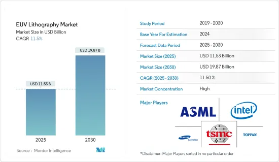
预计 2025 年 EUV微影术市场规模为 115.3 亿美元,到 2030 年将达到 198.7 亿美元,预测期内(2025-2030 年)的复合年增长率为 11.5%。
EUV微影术使用的光波长仅 13.5nm。这比先进晶片製造中的另一种微影术技术——使用 193nm 光的深紫外光微影术的波长短近 14 倍。该技术能够更精确、更有效率地生产节点尺寸为 7nm 的半导体,甚至小至 5nm 的电晶体规模。
主要亮点
- 随着半导体尺寸不断缩小,采用 EUV微影术技术变得越来越重要。 EUV微影术技术能够实现晶圆上复杂图案的微型化,为5G、AI、汽车等次世代应用程式提供最佳且高效的选择。借助 EUV 技术,EUV 光的短波长使得列印与先进技术相关的设计的奈米级特征成为可能,使晶片製造商能够继续推动晶片小型化。
- 台积电的极紫外线 (EUV) 工具预计将达到生产成熟度,工具运转率已达到量产目标,并在常规运行中提供超过 250 瓦的功率输出。晶片製造商正在寻求利用 EUV 来实现 7nm、5nm 及更先进的逻辑,目前没有其他选择。下一代微影术技术尚未准备好,无法应用于7nm和5nm规模。对于 3nm 及以上,晶片製造商希望使用高 NA EUV,但开发这项技术仍面临一些挑战。
- 台积电也计划在 2022 年开始量产 3nm 产品。另一家主要企业三星电子则计划在 2030 年之前在极紫外线 (EUV)微影术技术方面超越台积电。台积电先前在 2019 年 12 月宣布,将于 2020 年上半年开始供应 5nm 製程晶片,并于 2022 年开始量产 3nm 製程晶片。该公司还预计在 2024 年开始生产 2nm 製程产品。
- 受新冠疫情影响,ASML 的设备出口出现困难,对三星电子、台积电等全球主要半导体製造商产生了不利影响。该公司的设备交付延迟迫使两家公司改变其策略发展和生产蓝图。公司设备交付的延迟迫使两家公司改变其策略发展和生产计画。台积电延后了3奈米半导体的试产。同时,三星电子原计划于 2020 年开始商业化生产 5nm 半导体,但直到 2021 年底才得以实现。
EUV微影术市场趋势
铸件製造商预计将占据较大份额
- 台积电计画于2022年开始量产3nm产品,因而称霸全球晶圆代工厂市场。市场落后的三星电子则计划在2030年极紫外线(EUV)微影术技术方面超越台积电。 2019年12月,台积电宣布将于2020年上半年开始供应5nm製程晶片,并于2022年开始量产3nm製程晶片。同时,台积电也预计2024年开始生产2nm製程产品。
- 三星在市场上面临一系列挑战。例如,用于 EUV微影术的光阻剂供应可能受到日本出口管制。此外,还有相当多的公司正在试图与三星电子竞争。中国大陆和台湾的半导体公司合作日益密切。三星电子不断推出新的微製造技术,如 FinFET、环栅和多桥通道 FET,以与越来越多的竞争对手竞争。
- 2021 年 2 月,三星代工向亚利桑那州、纽约州和德克萨斯州的当局提交了文件,寻求在美国建立一座尖端半导体製造工厂。该工厂将建在德克萨斯州奥斯汀附近,预计耗资超过 170 亿美元,并创造 1,800 个就业机会。如果一切按计划进行,该代工厂预计将于 2023 年第四季运作。该公司并未透露将针对哪种製程节点进行设计,但这家新晶圆厂很引人注目。
- 台湾半导体製造公司(TSMC)和联华电子公司(UMC)等供应商已宣布,他们正专注于转移生产,以满足大众和丰田等汽车製造商的需求。此外,高通和苹果等公司的需求导致半导体供应延迟。 《汽车新闻》的一项新调查(2021 年 4 月)显示,53% 的受访者在美国境外采购晶片,55% 的製造商正在寻找海外替代晶片采购。
- 这些因素导致新公司进入研究市场。例如,英特尔最近宣布推出一项新业务——英特尔代工服务,以满足汽车製造商的需求。同样,2021年3月,World Castings表示将投资14亿美元在全球扩大产能,以协助福特、福斯和通用汽车等汽车製造商削减产量。
预计亚太地区将占很大份额
- 亚太地区持续占据全球极紫外线(EUV)微影术市场的最大收入份额。预计台湾将在预测期内占据该地区的主导地位。台积电在台湾的业务扩张以及加大对EUV微影术技术的投资是支撑台湾极紫外光微影术市场成长的最重要因素之一。台湾占据了亚太地区EUV微影术市场的大部分收益占有率。除台湾以外,日本、中国和韩国的极紫外光微影术市场预计将在未来几年为相关人员提供重大机会。
- 随着美国贸易摩擦加剧,中国半导体厂商也利用二手晶片製造设备加速生产自家产品,推高了日本二手市场的设备价格。日本二手设备经销商表示,价格比去年上涨了 20%。老一辈的机器不受美国美国制裁的限制,所以中国玩家可以自由使用。
- 由于冠状病毒大流行而倾向于待在室内也是一个因素。随着全球对晶片的需求不断增长,即使是不太先进的设备也卖得非常火爆。因此,汽车用半导体的供不应求有可能将长期持续。
- ASML 的新训练设施可能对两家公司都有好处。该公司是欧洲最大的半导体机械品牌,但台湾製造商是其最大客户。根据《亚洲日经评论》报道,ASML今年计画出货的35台EUV系统当中,有20台是为台积电提供的。荷兰公司 ASML 正在为晶片製造商的员工提供更多工具熟悉度,为未来的销售做准备。 ASML 还计划在台湾开设一个新的研发机构,到 2023 年将本地员工人数增加到 500 多人。
EUV微影术产业概况
EUV微影术市场高度整合,因为 ASML 是唯一一家使用极紫外光的微影术设备製造商。该公司为世界各地的半导体製造商生产和销售设备,其中包括英特尔、三星和台湾半导体製造股份有限公司 (TSMC)。该公司近25%的企业收益来自EUV光刻工具的销售,反映了该公司在EUV光刻工具製造和商业化方面的主导地位。
- 2021年12月欧洲新星ASML正在研发新版极紫外光微影术设备。该设备用于将图案切割成硅块,以製造世界上最复杂的处理器。三星、台积电和英特尔正在使用该公司目前的 EUV 设备为下一代电脑和智慧型手机製造晶片。
- 2021年3月三星将增加EUV扫描器的产量,以与全球最大的代工厂台积电竞争。与传统设备不同,EUV 扫描器有可能透过减少生产更小电路所需的微影术步骤来简化晶片製造流程,从而引发主要晶片製造商对该技术的竞相争夺。
其他福利:
- Excel 格式的市场预测 (ME) 表
- 3个月的分析师支持
目录
第一章 引言
- 研究假设和市场定义
- 研究范围
第二章调查方法
第三章执行摘要
第四章 市场洞察
- 市场概览
- 产业价值链分析
- 产业吸引力-波特五力分析
- 供应商的议价能力
- 买家的议价能力
- 新进入者的威胁
- 替代品的威胁
- 竞争对手之间的竞争强度
- COVID-19 产业影响评估
第五章市场动态
- 市场驱动因素
- 与其他技术相比,该技术可以更快地生产微晶片
- 晶片製造商减少製造步骤以提高效率
- 市场限制
- 使用 EUV 雷射器替换现有深紫外线雷射的高成本
- 市场垄断
- 技术简介
第六章市场区隔
- 产品类型
- 光源
- 镜子
- 面具
- 类型
- 铸件
- 集成设备製造商 (IDM)
- 地区
- 韩国
- 台湾
- 其他的
第七章竞争格局
- 公司简介
- ASML Holding NV
- NTT Advanced Technology Corporation
- Canon Inc.
- Nikon Corporation
- Intel Corporation
- Taiwan Semiconductor Manufacturing Company Limited
- Samsung Electronics Co. Ltd
- Toppan Photomasks Inc.
- Ushio, Inc.
第八章投资分析
第九章:市场的未来
The EUV Lithography Market size is estimated at USD 11.53 billion in 2025, and is expected to reach USD 19.87 billion by 2030, at a CAGR of 11.5% during the forecast period (2025-2030).
EUV lithography makes the usage of light with a wavelength of just 13.5 nm, which is a reduction of almost 14 times the wavelength of the other lithography techniques in advanced chipmaking, Deep Ultraviolet lithography, which uses 193 nm light. ASML, which is the dominant player in the market, has been exploring ways to reduce transistor sizes and has made considerable strides in the field of EUV lithography, which enables more precise and efficient production of semiconductors at small transistor scales around 7nm node size or even 5nm.
Key Highlights
- As semiconductor geometries tend to grow smaller and smaller, the adoption of EUV lithography technology has become extremely important, as it enables scaling down of intricate patterns on wafers by providing an optimal and efficient choice for next-generation applications, including 5G, AI, and Automotive. EUV technology allows the chip makers to keep driving chip scaling as the shorter wavelength of EUV light is capable of printing the nanometer-scale features of the designs related to the advanced techniques.
- TSMC's Extreme Ultraviolet (EUV) tools are expected to reach production maturity, with tool availability already reaching target goals for high-volume production and output power of greater than 250 watts for daily operations. Chipmakers are banking on EUV at 7nm, 5nm, and beyond for leading-edge logic, and today there are no other options available. The next-generation lithography technologies are not ready and can not be applied at 7nm and 5nm scales. At 3nm and beyond, chipmakers hope to use high-NA EUV, but several challenges have yet to be overcome in developing this technology.
- TSMC has also been planning to start the volume production of the 3-nm products by 2022. Samsung Electronics Co. Ltd, another major player in the market, aims to overtake TSMC by 2030 with its extreme ultraviolet (EUV) lithography technology. TSMC, previously in Dec 2019, announced that the company would be starting to supply 5 Nm process-based chips in the first half of 2020 and will be starting mass production of 3-nm process chips in 2022. The company also anticipates producing 2-nm process products by 2024.
- ASML faced difficulty exporting its equipment due to COVID-19, negatively affecting major global semiconductor producers, including Samsung Electronics and TSMC. A delay in the company's equipment delivery is forcing the two companies to change their strategic development and production roadmaps. Due to a delay in the delivery of the company's equipment, the two companies have to alter their strategic development and production plans. TSMC has postponed the test production of 3-nm semiconductors. Samsung Electronics, meantime, had hoped to commence commercial production of 5-nm semiconductors in 2020 but was unable to do so until late 2021.
EUV Lithography Market Trends
Foundry is Expected to Hold Major Share
- TSMC is planning to dominate the global foundry market by starting the volume production of 3-nm products in 2022. Samsung Electronics Co, Ltd, the runner-up in the market, is aiming to overtake TSMC in 2030 with its extreme ultraviolet (EUV) lithography technology. TSMC announced in December 2019 that the company would start to supply 5-nm process-based chips in the first half of 2020 and start the mass production of 3-nm process chips in 2022. The company also expects o produce 2-nm process products in 2024.
- Samsung is facing a series of challenges in the market. For instance, the supply of photoresists for EUV lithography purposes can be subject to Japan's export restrictions. Besides, a significant number of companies are trying to compete with Samsung Electronics. Chinese and Taiwanese semiconductor companies are increasingly collaborating. Samsung Electronics has unveiled a series of new microfabrication techniques such as FinFET, gate-all-around, and multi-bridge-channel FET to compete with the increasing competitors.
- In February 2021, Samsung Foundry filed documents with authorities in Arizona, New York, and Texas seeking to build a leading-edge semiconductor manufacturing facility in the United States. The potential fab near Austin, Texas, is expected to cost over USD 17 billion and create 1,800 jobs. If everything goes as planned, the foundry will go online by the fourth quarter of 2023. There is an intrigue about the new fab, though the company did not state which process node it will be designed for.
- Vendors, such as Taiwan Semiconductor Manufacturing Co. (TSMC) and United Microelectronics Corp. (UMC), announced that they have been focusing on relocating their production to meet the demand from automakers, such as Volkswagen and Toyota, among others. In addition, the demand coming from companies, such as Qualcomm and Apple, has been creating delays in the supply of semiconductors. According to a new survey by Automotive News (April 2021), 53% of the respondents suggested that they source their chips from outside the United States, and 55% of the manufacturers have been looking for alternative chip sources outside the country.
- Such factors have been leading to the entry of new companies into the market studied. For instance, recently, Intel announced the launch of a new business Intel Foundry Services, to meet the demand for automotive manufacturers. Similarly, in March 2021, Global Foundries announced that it has been planning to invest USD 1.4 billion for capacity expansion in different parts of the world to support automakers cutting output, such as Ford, Volkswagen, and General Motors.
Asia Pacific is Expected to Hold Major Share
- The Asia Pacific continues to hold the largest revenue share in the global market for Extreme Ultraviolet (EUV) lithography. Taiwan is expected to have an edge in the region over the forecast period. TSMC's expansion in Taiwan and its increasing investments in the EUV lithography technology is among the most critical factors instrumental in the growth of the Extreme Ultraviolet lithography market in Taiwan. The country accounts for the majority revenue share of the market for EUV lithography in the Asia Pacific region. Apart from Taiwan, the Extreme Ultraviolet lithography markets in Japan, China, and South Korea are expected to create significant opportunities for stakeholders in the coming years.
- Chinese semiconductor makers are also utilizing used chipmaking machines as they rush to produce homegrown products amid US-Sino trade tensions, driving up equipment prices in Japan's secondary market. Japanese used equipment dealers say prices are up by 20% from last year. Older-generation machines are not restricted by the United States sanctions on China, giving Chinese players unfettered access.
- The stay-at-home trend spurred by the coronavirus pandemic is also a factor. As chip demand rises worldwide, even equipment that is not the most up-to-date is selling at a brisk pace. This, in turn, could prolong the shortage of semiconductors used in automobiles.
- ASML's new training complex will likely be beneficial to both companies. While the firm is Europe's largest semiconductor machinery brand, the Taiwanese manufacturer is its biggest customer. Asian Nikkei Review states that 20 of the 35 EUV systems ASML intends to ship this year are going to TSMC. The Dutch concern is setting up future sales by familiarizing more of the chipmaker's staff with its tools. ASML also plans on opening a new research and development facility in Taiwan, which will bring its local headcount over 500 by 2023.
EUV Lithography Industry Overview
The Extreme Ultraviolet Lithography Market is highly consolidated as ASML is the only manufacturer of lithography machines that use extreme ultraviolet light. The company manufactures and sells its tools to some global semiconductor fabricators, including Intel, Samsung, and Taiwan Semiconductor Manufacturing Company (TSMC). Almost 25% of the company's revenues are generated by sales of EUV lithography systems, which reflects the company's monopoly in the manufacturing and commercialization of EUV lithography systems.
- December 2021: ASML, a hot stock in Europe, is working on a new version of their extreme ultraviolet lithography equipment, which is used to carve patterns into chunks of silicon that produce the world's most sophisticated processors. Samsung, TSMC, and Intel use the company's current EUV equipment to create chips for the next generation of computers and smartphones.
- March 2021: Samsung is increasing its EUV scanner production to compete with TSMC, the world's largest foundry. EUV scanners, unlike traditional machines, may streamline the chip fabrication process by lowering the number of photolithography procedures necessary to generate finer circuits, causing major chipmakers to compete for the technology.
Additional Benefits:
- The market estimate (ME) sheet in Excel format
- 3 months of analyst support
TABLE OF CONTENTS
1 INTRODUCTION
- 1.1 Study Assumptions and Market Definition
- 1.2 Scope of the Study
2 RESEARCH METHODOLOGY
3 EXECUTIVE SUMMARY
4 MARKET INSIGHTS
- 4.1 Market Overview
- 4.2 Industry Value Chain Analysis
- 4.3 Industry Attractiveness - Porter's Five Forces Analysis
- 4.3.1 Bargaining Power of Suppliers
- 4.3.2 Bargaining Power of Buyers
- 4.3.3 Threat of New Entrants
- 4.3.4 Threat of Substitute Products
- 4.3.5 Intensity of Competitive Rivalry
- 4.4 Assessment of COVID-19 Impact on the Industry
5 MARKET DYNAMICS
- 5.1 Market Drivers
- 5.1.1 The technology resulting in a faster output of microchips compared to others
- 5.1.2 Chip makers reducing the manufacturing process for better efficiency
- 5.2 Market Restraints
- 5.2.1 High cost involved in replacing the existing Deep UV with EUV lasers
- 5.2.2 Monopoly existing within the market
- 5.3 Technology Snapshot
6 MARKET SEGMENTATION
- 6.1 Product Type
- 6.1.1 Light Sources
- 6.1.2 Mirrors
- 6.1.3 Masks
- 6.2 Type
- 6.2.1 Foundry
- 6.2.2 Integrated Device Manufacturers (IDMs)
- 6.3 Geography
- 6.3.1 South Korea
- 6.3.2 Taiwan
- 6.3.3 Others
7 COMPETITIVE LANDSCAPE
- 7.1 Company Profiles
- 7.1.1 ASML Holding NV
- 7.1.2 NTT Advanced Technology Corporation
- 7.1.3 Canon Inc.
- 7.1.4 Nikon Corporation
- 7.1.5 Intel Corporation
- 7.1.6 Taiwan Semiconductor Manufacturing Company Limited
- 7.1.7 Samsung Electronics Co. Ltd
- 7.1.8 Toppan Photomasks Inc.
- 7.1.9 Ushio, Inc.
8 INVESTMENT ANALYSIS
9 FUTURE OF THE MARKET
 雷射气体光刻市场分析及预测(至2035年):依类型、产品类型、服务、技术、组件、应用、材料类型、製程、最终用户及设备划分
 极紫外线 (EUV) 微影市场:依设备(曝光系统、光源、光学元件和反射镜、掩模相关系统)、技术(标准 EUV/NXE、高数值孔径 EUV/EXE)和应用(代工厂、记忆体、整合装置製造商)划分 - 全球预测至 2036 年
 全球极紫外光刻市场规模、份额、趋势和成长分析报告(2026-2034年)
 极紫外线(EUV)微影术市场:按组件、系统类型、最终用户、应用和地区分類的全球市场-预测至2032年
 全球极微影术元件市场:预测(至2034年)-按装置类型、材料类型、技术、应用、最终使用者和地区分類的分析
 2026年全球极紫外光微影市场报告
 半色调掩模市场按掩模类型、最终用途行业和分销管道划分 - 全球预测 2026-2032极紫外平面镜市场:依基板、镀膜材料、应用及通路划分,全球预测(2026-2032年)极紫外光刻 (EUV) 市场规模、占有率、成长及全球产业分析:按类型、应用和地区划分的洞察与预测 (2026-2034)
 极紫外光刻市场-全球产业规模、份额、趋势、机会及预测(依技术节点、组件类型、终端用户产业、区域及竞争格局划分,2021-2031年预测)