


 |
市场调查报告书
商品编码
1740912
雷射光刻系统市场机会、成长动力、产业趋势分析及 2025 - 2034 年预测Laser Lithography Systems Market Opportunity, Growth Drivers, Industry Trend Analysis, and Forecast 2025 - 2034 |
||||||
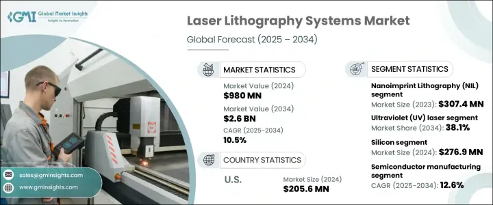
2024 年,全球雷射光刻系统市场规模达 9.8 亿美元,预计到 2034 年将以 10.5% 的复合年增长率成长,达到 26 亿美元,这主要得益于市场对更强大、更紧凑、更节能的半导体装置日益增长的需求。随着半导体技术的进步不断突破微型化和性能的界限,该市场正获得显着发展动能。随着晶片製造商积极追求更小的节点,雷射光刻系统(尤其是深紫外线 (DUV) 和极紫外线 (EUV) 系统)对于提供下一代生产所需的精度和可扩展性至关重要。人工智慧、电信和高效能消费性电子产品领域正在向 10 奈米以下技术转变,凸显了对超高精度图案化解决方案的需求。
随着摩尔定律持续推动製造商创新,雷射光刻技术为大规模生产复杂、高密度元件提供了技术支撑。研发投入、5G基础设施的普及、物联网的扩展以及光子学日益融入主流应用,进一步增强了市场前景。晶片製造领域对永续性和能源效率的日益重视,也有利于先进的光刻解决方案,推动了从传统方法向基于雷射的系统显着转变,该系统可提供更高的吞吐量、更低的缺陷率和更好的材料利用率。
| 市场范围 | |
|---|---|
| 起始年份 | 2024 |
| 预测年份 | 2025-2034 |
| 起始值 | 9.8亿美元 |
| 预测值 | 26亿美元 |
| 复合年增长率 | 10.5% |
随着 10 奈米以下节点技术在人工智慧、电信和高性能消费性电子产品中的应用日益广泛,雷射光刻——深紫外线 (DUV) 和极紫外线 (EUV) 系统——已成为实现晶片精密图案化的关键。随着半导体製造商不断缩小电晶体尺寸以遵循摩尔定律,下一代光刻解决方案需要提供维持生产效率和满足市场需求所需的精度和分辨率。
系统单晶片 (SoC) 和光子积体电路 (PIC) 等整合系统的兴起带来了新的设计挑战,只有采用高度先进的雷射光刻技术才能应对。这些电路需要卓越的图案化精度,尤其是在医疗诊断、电信和汽车安全系统等应用领域。光波导、微光学元件和感测器等光子和光电子装置依赖超精密的製造製程。雷射光刻技术的创新使得建构用于快速资料通讯、雷射雷达 (LiDAR) 技术和高解析度医学成像的奈米结构成为可能。
2024年,雷射光刻系统市场中硅晶片的部分规模达到2.769亿美元。由于硅片与CMOS製程的出色相容性、成本效益以及优异的电气特性,它仍然是整个半导体产业的首选基板。随着先进电子产品规模的不断扩大,硅片在逻辑电路、微控制器和储存晶片中的广泛应用确保了其稳定的需求。随着人工智慧运算、资料中心和下一代行动装置等领域对精度的要求日益提高,硅片的多功能性使其能够支援高密度、高速的元件。
预计半导体製造领域将迎来强劲发展势头,2025 年至 2034 年期间的复合年增长率将达到 12.6%。这一增长与高效能运算、人工智慧晶片以及需要奈米级超精细图案化的下一代记忆体解决方案日益增长的需求密切相关。雷射光刻技术,尤其是使用 EUV(极紫外线)和 DUV(深紫外线)技术的雷射光刻技术,是这些技术进步的核心。这些系统可实现 5 奈米以下节点的生产,这是突破摩尔定律极限的关键基准。
在政府大力推动半导体生产回流政策的推动下,美国雷射光刻系统市场规模在2024年达到2.056亿美元。联邦政府的资金投入和跨部门合作正在加速奈米製造技术的突破,使美国成为技术进步的关键枢纽。
Raith GmbH、海德堡仪器和 KLA Corporation 等领先企业的关键策略包括增强研发能力、与研究机构合作以及扩大生产能力。这些公司正在投资超解析度雷射系统,并针对 10 奈米以下製造、PIC 生产和混合封装等高成长领域优化其产品。此外,与半导体代工厂的合作也有助于这些公司在高度动态的市场中保持敏捷。
目录
第一章:方法论与范围
第二章:执行摘要
第三章:行业洞察
- 产业生态系统分析
- 影响价值链的因素
- 利润率分析
- 中断
- 未来展望
- 製造商
- 经销商
- 川普政府关税对飞机零件的影响分析
- 对贸易的影响
- 贸易量中断
- 报復措施
- 对产业的影响
- 供给侧影响
- 价格波动
- 供应链重组
- 生产成本影响
- 需求面影响
- 价格传导至终端市场
- 消费者反应模式
- 供给侧影响
- 受影响的主要公司
- 策略产业回应
- 供应链重组
- 定价和产品策略
- 政策参与
- 展望与未来考虑
- 对贸易的影响
- 供应商格局
- 利润率分析
- 重要新闻和倡议
- 监管格局
- 衝击力
- 成长动力
- 半导体小型化需求不断成长
- 极紫外线 (EUV) 微影技术的进步
- 光子学和光电子学领域的应用日益广泛
- 先进封装技术的扩展
- 政府对半导体製造的支持
- 产业陷阱与挑战
- 资本和营运成本高
- 技术复杂性和工艺限制
- 成长动力
- 成长潜力分析
- 波特的分析
- PESTEL分析
第四章:竞争格局
- 介绍
- 公司市占率分析
- 竞争定位矩阵
- 战略展望矩阵
第五章:市场估计与预测:依技术类型,2021-2034
- 主要趋势
- 直接雷射写入(DLW)
- 干涉光刻
- 奈米压印微影术(NIL)
- 双光子聚合(2PP)
第六章:市场估计与预测:按雷射光源,2021-2034 年
- 主要趋势
- 准分子雷射
- 二极体雷射
- 飞秒雷射
- 紫外线(UV)激光
第七章:市场估计与预测:依基材类型,2021-2034
- 主要趋势
- 硅
- 玻璃
- 聚合物
- 金属
第 8 章:市场估计与预测:按应用,2021 年至 2034 年
- 主要趋势
- 半导体製造
- 微电子
- 光子装置
- 微流体
- 显示器技术(OLED、MicroLED、LCD 等)
- 奈米科技研究
- 生物技术和医疗器械
第九章:市场估计与预测:依最终用途产业,2021-2034 年
- 主要趋势
- 电子和半导体
- 医疗保健和生物医学
- 航太与国防
- 汽车
- 电信
- 其他的
第十章:市场估计与预测:按地区,2021-2034
- 主要趋势
- 北美洲
- 我们
- 加拿大
- 欧洲
- 英国
- 德国
- 法国
- 义大利
- 西班牙
- 俄罗斯
- 亚太地区
- 中国
- 印度
- 日本
- 韩国
- 澳洲
- 拉丁美洲
- 巴西
- 墨西哥
- MEA
- 南非
- 沙乌地阿拉伯
- 阿联酋
第 11 章:公司简介
- ADVANTEST CORPORATION
- AGC Inc.
- ASML Holding NV
- Carl Zeiss AG
- Edmund Optics Inc.
- Energetiq Technology, Inc.
- Finisar
- Heidelberg Instruments
- HOYA Corporation
- INTEGRATED DYNAMICS ENGINEERING GmbH
- KLA Corporation
- Lasertec Corporation
- NTT Advanced Technology Corporation
- NuFlare Technology Inc.
- Onto Innovation Inc.
- Photronics, Inc.
- Raith GmbH
- Rigaku Holdings Corporation
- Sono-Tek Corporation
- SUSS MicroTec SE
- TOPPAN Inc.
- TRUMPF
- TSI
- Ushio Inc.
- Veeco Instruments, Inc.
The Global Laser Lithography Systems Market was valued at USD 980 million in 2024 and is estimated to grow at a CAGR of 10.5% to reach USD 2.6 billion by 2034, driven by the rising demand for more powerful, compact, and energy-efficient semiconductor devices. The market is gaining significant momentum as advancements in semiconductor technology push the boundaries of miniaturization and performance. With chipmakers aggressively pursuing smaller nodes, the role of laser lithography systems-especially deep ultraviolet (DUV) and extreme ultraviolet (EUV) systems-has become critical for delivering the precision and scalability needed for next-generation production. The ongoing shift toward sub-10nm technologies across artificial intelligence, telecommunications, and high-performance consumer electronics underscores the need for ultra-accurate patterning solutions.
As Moore's Law continues to pressure manufacturers to innovate, laser lithography provides the technological backbone for producing complex, high-density devices at scale. Investments in R&D, rising adoption of 5G infrastructure, IoT expansion, and the increasing integration of photonics into mainstream applications further strengthen the market outlook. The growing emphasis on sustainability and energy efficiency in chip manufacturing also favors advanced lithography solutions, driving a notable shift from traditional methods to laser-based systems that offer higher throughput, lower defect rates, and better material utilization.
| Market Scope | |
|---|---|
| Start Year | 2024 |
| Forecast Year | 2025-2034 |
| Start Value | $980 Million |
| Forecast Value | $2.6 Billion |
| CAGR | 10.5% |
With the increasing adoption of sub-10nm node technology in artificial intelligence, telecommunications, and high-performance consumer electronics, laser lithography-deep ultraviolet (DUV) and extreme ultraviolet (EUV) systems-has become vital for precision chip patterning. As semiconductor manufacturers continue shrinking transistor dimensions to adhere to Moore's Law, next-generation lithography solutions offer the accuracy and resolution needed to sustain production efficiency and meet market demand.
The rise of integrated systems such as system-on-chip (SoC) and photonic integrated circuits (PICs) presents new design challenges that can only be addressed with highly advanced laser-based lithography techniques. These circuits demand exceptional patterning accuracy, especially as they are used in applications ranging from healthcare diagnostics to telecommunications and automotive safety systems. Photonic and optoelectronic devices, such as optical waveguides, micro-optics, and sensors, rely on ultra-precise fabrication processes. Innovations in laser lithography enable the construction of nanostructures used in fast data communication, LiDAR technologies, and high-resolution medical imaging.
The silicon segment in the laser lithography systems market reached USD 276.9 million in 2024. Silicon remains the preferred substrate across the semiconductor industry due to its excellent compatibility with CMOS processes, cost-effectiveness, and superior electrical characteristics. Its widespread use in logic circuits, microcontrollers, and memory chips ensures a steady demand as advanced electronics continue to scale. As precision requirements intensify in fields like AI computing, data centers, and next-generation mobile devices, silicon's versatility enables it to support high-density, high-speed components.
The semiconductor manufacturing segment is expected to experience strong momentum, with a projected CAGR of 12.6% between 2025 and 2034. This growth is closely linked to the rising demand for high-performance computing, AI chips, and next-gen memory solutions that require ultra-fine patterning at the nanoscale. Laser lithography, especially using EUV (extreme ultraviolet) and DUV (deep ultraviolet) technologies, is at the core of these advancements. These systems allow for sub-5nm node production, a critical benchmark in pushing the limits of Moore's Law.
United States Laser Lithography Systems Market reached USD 205.6 million in 2024, supported by robust government policies focused on reshoring semiconductor production. Federal funding and cross-sector partnerships are accelerating breakthroughs in nanofabrication, making the country a critical hub for technological advancement.
Key strategies among leading players-Raith GmbH, Heidelberg Instruments, KLA Corporation-include expanding R&D capabilities, collaborating with research institutes, and scaling manufacturing capacity. Companies are investing in ultra-resolution laser systems and optimizing their offerings for high-growth areas like sub-10nm fabrication, PIC production, and hybrid packaging. Additionally, partnerships with semiconductor foundries are helping these firms remain agile in a highly dynamic market.
Table of Contents
Chapter 1 Methodology & Scope
- 1.1 Market scope & definitions
- 1.2 Base estimates & calculations
- 1.3 Forecast calculations
- 1.4 Data sources
- 1.4.1 Primary
- 1.4.2 Secondary
- 1.4.2.1 Paid sources
- 1.4.2.2 Public sources
Chapter 2 Executive Summary
- 2.1 Industry synopsis, 2021-2034
Chapter 3 Industry Insights
- 3.1 Industry ecosystem analysis
- 3.1.1 Factor affecting the value chain
- 3.1.2 Profit margin analysis
- 3.1.3 Disruptions
- 3.1.4 Future outlook
- 3.1.5 Manufacturers
- 3.1.6 Distributors
- 3.2 Trump Administration Tariffs Impact Analysis on Aircraft Components
- 3.2.1 Impact on Trade
- 3.2.1.1 Trade Volume Disruptions
- 3.2.1.2 Retaliatory Measures
- 3.2.1.3 Impact on the Industry
- 3.2.1.3.1 Supply-Side Impact
- 3.2.1.3.1.1 Price Volatility
- 3.2.1.3.1.2 Supply Chain Restructuring
- 3.2.1.3.1.3 Production Cost Implications
- 3.2.1.3.2 Demand-Side Impact
- 3.2.1.3.2.1 Price Transmission to End Markets
- 3.2.1.3.2.2 Consumer Response Patterns
- 3.2.1.3.1 Supply-Side Impact
- 3.2.1.4 Key Companies Impacted
- 3.2.1.5 Strategic Industry Responses
- 3.2.1.5.1 Supply chain reconfiguration
- 3.2.1.5.2 Pricing and product strategies
- 3.2.1.5.3 Policy engagement
- 3.2.1.6 Outlook and future considerations
- 3.2.1 Impact on Trade
- 3.3 Supplier landscape
- 3.4 Profit margin analysis
- 3.5 Key news & initiatives
- 3.6 Regulatory landscape
- 3.7 Impact forces
- 3.7.1 Growth drivers
- 3.7.1.1 Rising demand for semiconductor miniaturization
- 3.7.1.2 Advancements in Extreme Ultraviolet (EUV) lithography
- 3.7.1.3 Growing adoption in photonics and optoelectronics
- 3.7.1.4 Expansion of advanced packaging technologies
- 3.7.1.5 Government support for semiconductor manufacturing
- 3.7.2 Industry pitfalls & challenges
- 3.7.2.1 High capital and operational costs
- 3.7.2.2 Technical complexity and process limitations
- 3.7.1 Growth drivers
- 3.8 Growth potential analysis
- 3.9 Porter's analysis
- 3.10 PESTEL analysis
Chapter 4 Competitive Landscape, 2024
- 4.1 Introduction
- 4.2 Company market share analysis
- 4.3 Competitive positioning matrix
- 4.4 Strategic outlook matrix
Chapter 5 Market Estimates & Forecast, By Technology Type, 2021-2034 (USD Million)
- 5.1 Key trends
- 5.2 Direct Laser Writing (DLW)
- 5.3 Interference lithography
- 5.4 Nanoimprint Lithography (NIL)
- 5.5 Two-Photon Polymerization (2PP)
Chapter 6 Market Estimates & Forecast, By Laser Source, 2021-2034 (USD Million)
- 6.1 Key trends
- 6.2 Excimer laser
- 6.3 Diode laser
- 6.4 Femtosecond laser
- 6.5 Ultraviolet (UV) laser
Chapter 7 Market Estimates & Forecast, By Substrate Type, 2021-2034 (USD Million)
- 7.1 Key trends
- 7.2 Silicon
- 7.3 Glass
- 7.4 Polymers
- 7.5 Metal
Chapter 8 Market Estimates & Forecast, By Application, 2021-2034 (USD Million)
- 8.1 Key trends
- 8.2 Semiconductor manufacturing
- 8.3 Microelectronics
- 8.4 Photonic Devices
- 8.5 Microfluidics
- 8.6 Display Technology (OLED, MicroLEDs, LCDs, etc.)
- 8.7 Nanotechnology research
- 8.8 Biotechnology & medical devices
Chapter 9 Market Estimates & Forecast, By End Use Industry, 2021-2034 (USD Million)
- 9.1 Key trends
- 9.2 Electronics & semiconductor
- 9.3 Healthcare & biomedical
- 9.4 Aerospace & defense
- 9.5 Automotive
- 9.6 Telecommunications
- 9.7 Others
Chapter 10 Market Estimates & Forecast, By Region, 2021-2034 (USD Million)
- 10.1 Key trends
- 10.2 North America
- 10.2.1 U.S.
- 10.2.2 Canada
- 10.3 Europe
- 10.3.1 UK
- 10.3.2 Germany
- 10.3.3 France
- 10.3.4 Italy
- 10.3.5 Spain
- 10.3.6 Russia
- 10.4 Asia Pacific
- 10.4.1 China
- 10.4.2 India
- 10.4.3 Japan
- 10.4.4 South Korea
- 10.4.5 Australia
- 10.5 Latin America
- 10.5.1 Brazil
- 10.5.2 Mexico
- 10.6 MEA
- 10.6.1 South Africa
- 10.6.2 Saudi Arabia
- 10.6.3 UAE
Chapter 11 Company Profiles
- 11.1 ADVANTEST CORPORATION
- 11.2 AGC Inc.
- 11.3 ASML Holding N.V.
- 11.4 Carl Zeiss AG
- 11.5 Edmund Optics Inc.
- 11.6 Energetiq Technology, Inc.
- 11.7 Finisar
- 11.8 Heidelberg Instruments
- 11.9 HOYA Corporation
- 11.10 INTEGRATED DYNAMICS ENGINEERING GmbH
- 11.11 KLA Corporation
- 11.12 Lasertec Corporation
- 11.13 NTT Advanced Technology Corporation
- 11.14 NuFlare Technology Inc.
- 11.15 Onto Innovation Inc.
- 11.16 Photronics, Inc.
- 11.17 Raith GmbH
- 11.18 Rigaku Holdings Corporation
- 11.19 Sono-Tek Corporation
- 11.20 SUSS MicroTec SE
- 11.21 TOPPAN Inc.
- 11.22 TRUMPF
- 11.23 TSI
- 11.24 Ushio Inc.
- 11.25 Veeco Instruments, Inc.
 雷射气体光刻市场分析及预测(至2035年):依类型、产品类型、服务、技术、组件、应用、材料类型、製程、最终用户及设备划分
 极紫外线 (EUV) 微影市场:依设备(曝光系统、光源、光学元件和反射镜、掩模相关系统)、技术(标准 EUV/NXE、高数值孔径 EUV/EXE)和应用(代工厂、记忆体、整合装置製造商)划分 - 全球预测至 2036 年
 全球极紫外光刻市场规模、份额、趋势和成长分析报告(2026-2034年)
 极紫外线(EUV)微影术市场:按组件、系统类型、最终用户、应用和地区分類的全球市场-预测至2032年
 全球极微影术元件市场:预测(至2034年)-按装置类型、材料类型、技术、应用、最终使用者和地区分類的分析
 2026年全球极紫外光微影市场报告
 半色调掩模市场按掩模类型、最终用途行业和分销管道划分 - 全球预测 2026-2032极紫外平面镜市场:依基板、镀膜材料、应用及通路划分,全球预测(2026-2032年)极紫外光刻 (EUV) 市场规模、占有率、成长及全球产业分析:按类型、应用和地区划分的洞察与预测 (2026-2034)
 极紫外光刻市场-全球产业规模、份额、趋势、机会及预测(依技术节点、组件类型、终端用户产业、区域及竞争格局划分,2021-2031年预测)