


 |
市场调查报告书
商品编码
1849988
光电:市场份额分析、行业趋势、统计数据和成长预测(2025-2030 年)Photonics - Market Share Analysis, Industry Trends & Statistics, Growth Forecasts (2025 - 2030) |
||||||
※ 本网页内容可能与最新版本有所差异。详细情况请与我们联繫。
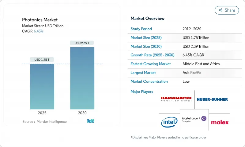
预计到 2025 年,光电市场规模将达到 1.75 兆美元,到 2030 年将达到 2.39 兆美元,复合年增长率为 6.43%。
资料中心内高速光链路的日益普及、汽车中雷射雷达(LiDAR)的渗透率不断提高以及对节能型LED照明的持续需求,共同推动了光子学领域的扩张。印度的生产关联激励计画(PLI)和欧盟的《晶片法案》等区域供应链计画正在加速新建晶圆厂的建设,而硅光电新兴企业的资金筹措也显示了市场对晶片间光互连技术的信心。汽车原始设备製造商(OEM)正将雷射雷达作为高级驾驶辅助系统(ADAS)的标配,推动了光子学产品销售的成长和成本的下降。同时,氮化镓(GaN)和微型LED产能的提升也凸显了市场正朝着降低消费和工业设备功耗的材料和装置方向发展。
全球光电市场趋势与洞察
资料中心互连的兴起刺激了硅光电收发器的需求
人工智慧工作负载正在重塑超大规模资料中心,推动流量密度超越铜缆的承载极限。硅光电收发器的出货速率现已超过 1.6 Tbps,在伺服器机架内扩展了传输距离,同时降低了每位元能耗。将光子层和电子层共封装在 300 毫米晶圆上的代工平台,能够增加光纤数量并降低耦合损耗,从而促进其在解耦架构中的应用。多轮融资,每轮均超过 1.5 亿美元,印证了投资者对这一发展方向的信心。随着营运商升级到光纤网络,调製器、加速器和整合雷射的量产也得到推动,进一步强化了光电市场的成长循环。
中国汽车OEM厂商采用以雷射雷达为基础的ADAS系统
雷射雷达在价格分布车型的快速普及正在重塑高级驾驶辅助系统(ADAS)的成本曲线。到2024年12月,中国领先的供应商每月将出货超过10万台车顶式雷射雷达,占据全球33%的市场。与国内汽车製造商的伙伴关係正在拓展光达的应用范围,使其从高端SUV扩展到C级车,并推动零件标准化,从而缩短认证週期。政府支持的安全标准正在加速产品上市,并树立了其他地区竞相效仿的典范。
化合物半导体晶圆瓶颈限制了成长
InP 和 GaN基板的可得性落后于资料中心雷射和射频功率元件的需求。少数几家代工厂控制着 150 毫米以下尺寸的基板供应,这增加了地震或设备故障导致供应中断的风险。虽然新的 CHIPS 法案资金正在支持德克萨斯州的产能扩张,但工具和製程的改进将前置作业时间延长至 2027 年,减缓了光电市场的成长势头。
细分市场分析
儘管基准,硅光电收发器预计仍将以 8.1% 的复合年增长率 (CAGR) 成为所有装置类别中成长最快的。它们为伺服器、储存和加速器架构提供动力,这些架构必须以每秒Petabyte级的速度传输资料。早期实现共封装光元件的量产将降低每Gigabit位元的成本,并扩大其应用范围。代工厂在电子层和光子层厚度同步方面的蓝图将增加设计库,缩短原型製作时间,并使光电市场对云端营运商更具吸引力。
LED在照明和背光领域占据主导地位,预计到2024年将占据光电市场32%的份额。新兴的微型LED面板有望为电视、穿戴式装置和汽车仪錶板带来高亮度和长寿命。雷射二极体正在金属切割和积层製造领域取得进展,而光学感测器则满足了环境监测和智慧农业日益增长的需求。这些广泛的应用领域使光电市场多元化,从而缓解了单一应用领域内的週期性波动。
到2024年,硅将占据光电市场40.3%的份额,这得益于其成熟的设备和低成本的8吋晶圆。然而,氮化镓(GaN)装置预计将以9.3%的复合年增长率成长,在5G无线网路和电动车动力传动系统所需的高频率和高电压下,GaN元件能够实现更高的效率。欧洲一条200毫米GaN中试生产线以及美国联邦政府提供的950万美元製程开发津贴,正在推动该生态系统的发展。
玻璃、二氧化硅和聚合物平台扩展了光纤网络,并实现了灵活的成像阵列。 InP增益区和硅波导管的异质整合可製造出适用于共封装光学元件的低成本雷射阵列。研究人员正在利用低损耗的SiN层来扩展频谱覆盖范围,而聚合物在生物感测一次性抛弃式领域也越来越受欢迎。这种材料的多样性确保了光电市场始终以创新主导,而不会局限于单一基板。
产业领导者正在推行规模化和专业化扩大策略。 LED製造商将外延和封装生产线集中布局,以缩短物流时间;而收发器新兴企业则透过授权製程设计套件来利用现有代工厂的资源。企业併购,例如以7.285亿美元收购模组製造商,反映出市场对承包光连接产品组合的需求。组件製造商的蓝图越来越强调电子和光学元件的协同优化,凸显了融合设计架构将如何推动光电市场的发展。
不同基板的供应动态各不相同。硅晶圆的供应链充足,而半绝缘氮化镓基板的合格供应商数量较少,导致前置作业时间不稳定。平台融合正逐渐成为一种对冲策略。集成设备製造商可利用现有工具集,将晶粒晶片键结到硅载体上,或在QST1模板上沉积氮化镓。这些混合堆迭结构降低了每瓦光功率的资本支出,增强了光电市场的韧性。
区域分析
亚太地区,在中国大陆、台湾、日本和韩国等半导体产业丛集的驱动下,将引领光电市场,预计到2024年将占45.7%的营收份额。中国本土光达(LiDAR)领军企业将占据全球33%的销售份额,预计2024年出货量将超过150万台,凸显其强大的本土化规模生产能力。台湾的晶圆代工生态系统正在引领光电和电子学一体化平台的建设,确保关键智慧财产权即使在2025年2月地震导致工厂生产中断后仍能留在该地区。日本的玻璃和精密光学公司正在供应特殊基板,而韩国的显示器製造商正在扩大微型LED试点生产线。
北美在研发支出方面保持着较高的份额。 2025年2月,一家光连接模组新兴企业获得1.75亿美元的创业投资资金,凸显了投资者对能够降低资料中心能耗的硬体的浓厚兴趣。根据《晶片法案》(CHIPS Act),联邦政府的激励措施正将资金投入到磷化铟(InP)和硅磷化硅(SiPh)的试点生产线,从而拓展了国内光电领域的选择,使其不再局限于国防领域。欧洲正利用绿色交易」和《欧洲晶片法案》,在义大利建造一座价值20亿欧元的碳化硅(SiC)和氮化镓(GaN)巨型工厂,目标是到2030年将其製造业份额翻倍。
中东和非洲将以7.2%的复合年增长率实现最快的成长,这主要得益于光纤骨干网部署和太阳能发电厂监测的需求。南美经济体正在投资精密农业感测技术,该技术依赖本地组装的高光谱遥测成像器。在所有地区,微影术工具的贸易限制正在改变资本投资的时机。供应商正在透过采取双源策略来应对,从而保持光电市场的韧性。
其他福利:
- Excel格式的市场预测(ME)表
- 3个月的分析师支持
目录
第一章 引言
- 研究假设和市场定义
- 调查范围
第二章调查方法
第三章执行摘要
第四章 市场情势
- 市场概览
- 市场驱动因素
- 资料中心互连的成长推动了北美对硅光电收发器的需求
- 中国汽车OEM厂商采用以雷射雷达为基础的ADAS系统
- 欧盟绿色交易对微型LED和GaN晶圆厂的奖励
- 印度的生产关联激励计划促进了国内光电丛集的发展
- 美国和欧洲照护现场感测技术蓬勃发展
- 太空卫星卫星群星座投资-合格光电
- 市场限制
- 化合物半导体晶圆(InP、GaN,小于150毫米)的瓶颈
- 功率超过 10kW 的二极体雷射的温度控管限制
- 集成光学积体电路标准之间的互通性差距
- 中美贸易限制增加了工具製造商的资本投资风险
- 产业生态系分析
- 技术展望
- 波特五力分析
- 供应商的议价能力
- 买方的议价能力
- 新进入者的威胁
- 替代品的威胁
- 竞争对手之间的竞争
第五章 市场规模与成长预测
- 副产品
- 雷射
- 二极体雷射
- 光纤雷射
- 固态及其他
- LED
- 感测器和检测器
- 光纤和波导
- 调製器和开关
- 其他的
- 雷射
- 材料
- 硅
- 玻璃和二氧化硅
- 化合物半导体(InP、GaAs、GaN)
- 聚合物和塑料
- 其他的
- 波长
- 紫外线 (UV)
- 可见的
- 红外线的
- 按最终用户行业划分
- 消费性电子产品
- 航太与国防
- 显示与成像
- 太阳能发电
- LED照明
- 医疗器材和生物设备
- 工业和製造业
- 汽车(包括光达)
- 数据与通讯
- 其他的
- 按地区
- 北美洲
- 美国
- 加拿大
- 墨西哥
- 欧洲
- 德国
- 英国
- 法国
- 义大利
- 西班牙
- 其他欧洲地区
- 亚太地区
- 中国
- 日本
- 韩国
- 印度
- 东南亚
- 亚太其他地区
- 南美洲
- 巴西
- 其他南美洲
- 中东和非洲
- 中东
- 阿拉伯聯合大公国
- 沙乌地阿拉伯
- 其他中东地区
- 非洲
- 南非
- 其他非洲地区
- 北美洲
第六章 竞争情势
- 市场集中度
- 策略趋势
- 市占率分析
- 公司简介
- Hamamatsu Photonics KK
- Intel Corporation
- Nokia Corporation(Alcatel-Lucent)
- Coherent Corp.
- AMS OSRAM AG
- IPG Photonics Corp.
- Signify NV
- Lumentum Holdings Inc.
- Infinera Corp.
- NEC Corp.
- Corning Inc.
- Schott AG
- Thorlabs Inc.
- Jenoptik AG
- Trumpf Photonics GmbH
- Molex LLC
- Rockley Photonics Ltd.
- Innolume GmbH
- Aeva Technologies Inc.
- Broadcom Inc.(Silicon Photonics)
- Carl Zeiss AG(incl. Scantinel)
- Nikon Corp.
第七章 市场机会与未来展望
The photonics market is valued at USD 1.75 trillion in 2025 and is set to advance to USD 2.39 trillion by 2030 at a 6.43% CAGR.
Expansion rests on the rising deployment of high-speed optical links inside data centers, growing LiDAR penetration in vehicles and sustained demand for energy-efficient LED lighting. Regional supply-chain programs, such as India's PLI scheme and the EU Chips Act, are accelerating new fab construction, while corporate funding rounds for silicon-photonics start-ups signal confidence in chip-to-chip optical interconnects. Automotive OEMs are standardizing LiDAR as an ADAS staple, stimulating volume growth and cost declines. At the same time, GaN and micro-LED capacity ramp-ups underline the shift toward materials and devices that lower power budgets in consumer and industrial equipment.
Global Photonics Market Trends and Insights
Proliferation of data-center interconnect spurring silicon photonics transceiver demand
AI workloads are restructuring hyperscale data centers, pushing traffic density beyond copper's limits. Silicon photonics transceivers now ship with data-rates above 1.6 Tbps, cutting energy per bit while lengthening reach inside server racks. Foundry platforms that co-package photonic and electronic layers on 300 mm wafers allow high fiber counts and lower coupling loss, which eases adoption in disaggregated architectures. Multiple venture rounds exceeding USD 150 million each underscore investor conviction in this path. As operators upgrade to optical fabrics, they also stimulate volume production of modulators, drivers and integrated lasers, reinforcing the photonics market growth loop.
Adoption of LiDAR-based ADAS across Chinese automotive OEMs
Rapid LiDAR integration in mid-price vehicles is redefining ADAS cost curves. A leading Chinese supplier shipped more than 100,000 roof-mounted units monthly by December 2024, capturing 33% global share.Partnerships with domestic OEMs extend LiDAR coverage from premium SUVs to C-segment cars, triggering component standardization that shortens qualification cycles. Government-supported safety standards are accelerating time-to-market, creating a template other regions are starting to emulate.
Compound-semiconductor wafer bottlenecks constraining growth
InP and GaN substrate availability lags demand from data-center lasers and RF power devices. A handful of foundries control sub-150 mm supply, heightening disruption risks when earthquakes or equipment faults occur. While new CHIPS Act funding backs capacity expansions in Texas, tools and process qualifications stretch lead times into 2027, slowing the photonics market momentum.
Other drivers and restraints analyzed in the detailed report include:
- EU Green-Deal incentives for micro-LED and GaN photonics fabs
- India's PLI scheme catalyzing domestic photonics clusters
- Thermal-management limits hampering high-power laser development
For complete list of drivers and restraints, kindly check the Table Of Contents.
Segment Analysis
Silicon photonics transceivers hold a modest baseline but are forecast to expand at an 8.1% CAGR, the highest among device classes. They underpin server, storage and accelerator fabrics that must move petabytes every second. Early volume ramps in co-packaged optics bring down dollar-per-gigabit metrics, widening the adoption window. As foundry roadmaps sync electronic and photonic layer thicknesses, design libraries grow and time-to-prototype shortens, elevating the photonics market appeal for cloud operators.
LEDs, with 32% of 2024 photonics market share, dominate lighting and backlighting. Emerging micro-LED panels promise higher brightness and longer life for televisions, wearables and automotive clusters. Laser diodes penetrate metal cutting and additive manufacturing, while optical sensors tag rising demand for environmental monitoring and smart agriculture. The breadth of these categories keeps the photonics market diversified, cushioning cyclic swings in any single application group.
Silicon still accounts for 40.3% of the photonics market size in 2024, benefiting from mature equipment sets and low-cost eight-inch wafers. However, GaN devices, forecast to grow at 9.3% CAGR, attain higher efficiency at elevated frequencies and voltages, key for 5G radios and electric-vehicle powertrains. Subsidized 200 mm GaN pilot lines in Europe and US federal grants of USD 9.5 million for process development encourage ecosystem growth.
Glass, silica and polymer platforms expand fiber networks and enable flexible imaging arrays. Heterogeneous integration of InP gain sections with silicon waveguides produces low-cost laser arrays suited for co-packaged optics. Researchers exploit low-loss SiN layers to broaden spectral coverage, while polymers gain traction in biosensing disposables. Such material diversity ensures that the photonics market remains innovation-driven rather than locked to a single substrate.
Segment leaders pursue scale or specialization strategies. LED manufacturers co-locate epitaxy and packaging lines to cut logistics time, whereas transceiver start-ups license process design kits to tap established foundries. Corporate M&A, such as a USD 728.5 million module-maker acquisition, reflects the need for turnkey optical-connect portfolios. Component-maker roadmaps increasingly list co-optimization of electronics and optics, underscoring how converged design stacks propel the photonics market forward.
Supply dynamics vary by substrate. Silicon wafers draw on an abundant supply chain, whereas semi-insulating GaN substrates rely on fewer qualified suppliers, amplifying lead-time volatility. Platform convergence emerges as a hedge: integrated device manufacturers bond GaN dies on silicon carriers or deposit GaN on QST1 templates to benefit from existing toolsets. These hybrid stacks lower capex per watt of optical output, reinforcing the photonics market resilience.
The Photonics Market Report is Segmented by Product (Lasers, Leds, Sensors and Detectors, and More), Material (Silicon, Glass and Silica, and More), Wavelength (Ultraviolet, Visible, and Infrared), End-User Industry (Consumer Electronics, Aerospace and Defense, Display and Imaging, Solar Photovoltaics, LED Lighting, Medical and Bio-Instrumentation, and More), and Geography. The Market Forecasts are Provided in Terms of Value (USD).
Geography Analysis
Asia-Pacific led the photonics market with a 45.7% revenue share in 2024, fueled by semiconductor clusters in China, Taiwan, Japan and South Korea. China's domestic LiDAR champion recorded 33% global volume share and shipped more than 1.5 million units in 2024, underscoring local capacity to scale. Taiwan's foundry ecosystem pioneers integrated photonic-electronic platforms, ensuring that critical IP stays within regional boundaries even after the February 2025 earthquake disrupted fab output. Japan's glass and precision optics firms supply specialty substrates, while South Korean display makers expand micro-LED pilot lines.
North America maintains a high share of R&D expenditure. Venture funding of USD 175 million for an optical interconnect start-up in February 2025 highlighted investor appetite for hardware that cuts data-center power. Federal incentives under the CHIPS Act channel money toward InP and SiPh pilot lines, broadening domestic options beyond defense-specific photonics. Europe leverages the Green Deal and the European Chips Act to double manufacturing share by 2030, with a EUR 2 billion SiC and GaN megaplant in Italy among the flagship projects.
The Middle East and Africa post the fastest CAGR at 7.2%, driven by optical-fiber backbone rollouts and solar-farm monitoring needs. South American economies invest in precision-agriculture sensing that relies on hyperspectral imagers assembled locally. Across all regions, trade restrictions on lithography tools reshape capex timing. Suppliers respond by pursuing dual-source strategies, thereby preserving resilience in the photonics market.
- Hamamatsu Photonics KK
- Intel Corporation
- Nokia Corporation (Alcatel-Lucent)
- Coherent Corp.
- AMS OSRAM AG
- IPG Photonics Corp.
- Signify NV
- Lumentum Holdings Inc.
- Infinera Corp.
- NEC Corp.
- Corning Inc.
- Schott AG
- Thorlabs Inc.
- Jenoptik AG
- Trumpf Photonics GmbH
- Molex LLC
- Rockley Photonics Ltd.
- Innolume GmbH
- Aeva Technologies Inc.
- Broadcom Inc. (Silicon Photonics)
- Carl Zeiss AG (incl. Scantinel)
- Nikon Corp.
Additional Benefits:
- The market estimate (ME) sheet in Excel format
- 3 months of analyst support
TABLE OF CONTENTS
1 INTRODUCTION
- 1.1 Study Assumptions and Market Definition
- 1.2 Scope of the Study
2 RESEARCH METHODOLOGY
3 EXECUTIVE SUMMARY
4 MARKET LANDSCAPE
- 4.1 Market Overview
- 4.2 Market Drivers
- 4.2.1 Proliferation of data-center interconnect spurring silicon photonics transceiver demand in North America
- 4.2.2 Adoption of LiDAR-based ADAS across Chinese automotive OEMs
- 4.2.3 EU Green-Deal incentives for micro-LED and GaN photonics fabs
- 4.2.4 India's PLI scheme catalyzing domestic photonics clusters
- 4.2.5 Point-of-care biosensing surge in United States and Europe
- 4.2.6 Satellite mega-constellation investments in space-qualified photonics
- 4.3 Market Restraints
- 4.3.1 Compound-semiconductor wafer bottlenecks (InP, GaN <150 mm)
- 4.3.2 Thermal-management limits on >10 kW diode lasers
- 4.3.3 Interoperability gaps among integrated photonic IC standards
- 4.3.4 U.S.-China trade controls elevating cap-ex risk for tool makers
- 4.4 Industry Ecosystem Analysis
- 4.5 Technological Outlook
- 4.6 Porter's Five Forces Analysis
- 4.6.1 Bargaining Power of Suppliers
- 4.6.2 Bargaining Power of Buyers
- 4.6.3 Threat of New Entrants
- 4.6.4 Threat of Substitutes
- 4.6.5 Intensity of Competitive Rivalry
5 MARKET SIZE AND GROWTH FORECASTS (VALUES)
- 5.1 By Product
- 5.1.1 Lasers
- 5.1.1.1 Diode Lasers
- 5.1.1.2 Fiber Lasers
- 5.1.1.3 Solid-state and Others
- 5.1.2 LEDs
- 5.1.3 Sensors and Detectors
- 5.1.4 Optical Fibers and Waveguides
- 5.1.5 Modulators and Switches
- 5.1.6 Others
- 5.1.1 Lasers
- 5.2 By Material
- 5.2.1 Silicon
- 5.2.2 Glass and Silica
- 5.2.3 Compound Semiconductors (InP, GaAs, GaN)
- 5.2.4 Polymers and Plastics
- 5.2.5 Others
- 5.3 By Wavelength
- 5.3.1 Ultraviolet (UV)
- 5.3.2 Visible
- 5.3.3 Infrared
- 5.4 By End-user Industry
- 5.4.1 Consumer Electronics
- 5.4.2 Aerospace and Defense
- 5.4.3 Display and Imaging
- 5.4.4 Solar Photovoltaics
- 5.4.5 LED Lighting
- 5.4.6 Medical and Bio-instrumentation
- 5.4.7 Industrial and Manufacturing
- 5.4.8 Automotive (incl. LiDAR)
- 5.4.9 Data and Telecom
- 5.4.10 Others
- 5.5 By Geography
- 5.5.1 North America
- 5.5.1.1 United States
- 5.5.1.2 Canada
- 5.5.1.3 Mexico
- 5.5.2 Europe
- 5.5.2.1 Germany
- 5.5.2.2 United Kingdom
- 5.5.2.3 France
- 5.5.2.4 Italy
- 5.5.2.5 Spain
- 5.5.2.6 Rest of Europe
- 5.5.3 Asia-Pacific
- 5.5.3.1 China
- 5.5.3.2 Japan
- 5.5.3.3 South Korea
- 5.5.3.4 India
- 5.5.3.5 South East Asia
- 5.5.3.6 Rest of Asia-Pacific
- 5.5.4 South America
- 5.5.4.1 Brazil
- 5.5.4.2 Rest of South America
- 5.5.5 Middle East and Africa
- 5.5.5.1 Middle East
- 5.5.5.1.1 United Arab Emirates
- 5.5.5.1.2 Saudi Arabia
- 5.5.5.1.3 Rest of Middle East
- 5.5.5.2 Africa
- 5.5.5.2.1 South Africa
- 5.5.5.2.2 Rest of Africa
- 5.5.1 North America
6 COMPETITIVE LANDSCAPE
- 6.1 Market Concentration
- 6.2 Strategic Moves
- 6.3 Market Share Analysis
- 6.4 Company Profiles {(includes Global level Overview, Market level overview, Core Segments, Financials as available, Strategic Information, Market Rank/Share for key companies, Products and Services, and Recent Developments)}
- 6.4.1 Hamamatsu Photonics KK
- 6.4.2 Intel Corporation
- 6.4.3 Nokia Corporation (Alcatel-Lucent)
- 6.4.4 Coherent Corp.
- 6.4.5 AMS OSRAM AG
- 6.4.6 IPG Photonics Corp.
- 6.4.7 Signify NV
- 6.4.8 Lumentum Holdings Inc.
- 6.4.9 Infinera Corp.
- 6.4.10 NEC Corp.
- 6.4.11 Corning Inc.
- 6.4.12 Schott AG
- 6.4.13 Thorlabs Inc.
- 6.4.14 Jenoptik AG
- 6.4.15 Trumpf Photonics GmbH
- 6.4.16 Molex LLC
- 6.4.17 Rockley Photonics Ltd.
- 6.4.18 Innolume GmbH
- 6.4.19 Aeva Technologies Inc.
- 6.4.20 Broadcom Inc. (Silicon Photonics)
- 6.4.21 Carl Zeiss AG (incl. Scantinel)
- 6.4.22 Nikon Corp.
7 MARKET OPPORTUNITIES AND FUTURE OUTLOOK
- 7.1 White-space and Unmet-need Assessment
 光电晶片市场分析及预测(至2035年):类型、产品类型、技术、组件、应用、材料类型、装置、最终用户、功能
 光子学市场:依产品类型、应用和终端用户产业划分 - 至2036年的全球预测光电市场分析及预测(至2035年):依类型、产品类型、服务、技术、组件、应用、材料类型、装置、最终用户、功能划分
 美国光电:市场份额分析、行业趋势和统计数据、成长预测(2026-2031)
 光电市场-全球产业规模、份额、趋势、机会及预测(依产品类型、应用、最终用户、地区及竞争格局划分,2021-2031年)光电装置市场-全球产业规模、份额、趋势、预测及机会(按产品、应用、产业、地区及竞争格局划分),2021-2031年
 2026-2030年全球光电市场
 日本光子学市场报告(按类型、应用、最终用户和地区划分,2026-2034年)
 光电市场规模、份额和成长分析(按类型、应用、最终用途产业和地区划分)-产业预测,2026-2033年
 光电市场按产品类型、技术、应用、最终用户和分销管道划分-全球预测,2025-2032年