


 |
市场调查报告书
商品编码
1850222
自动测试机:市场占有率分析、产业趋势、统计数据和成长预测(2025-2030 年)Automated Test Equipment - Market Share Analysis, Industry Trends & Statistics, Growth Forecasts (2025 - 2030) |
||||||
※ 本网页内容可能与最新版本有所差异。详细情况请与我们联繫。
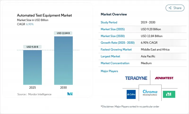
预计到 2025 年,自动化测试机市场规模将达到 92 亿美元,到 2030 年将达到 128.4 亿美元,年复合成长率为 6.9%。
需求成长的驱动力来自于向5奈米以下製程节点的过渡、汽车电气化以及系统级封装设计日益复杂的趋势。製造商正在投资研发能够测量10 nV/√Hz或更低杂讯的超低杂讯平台,而功率元件专家则指定使用能够安全施加超过1200V应力的测试仪。设备供应商同时也在整合即时数据分析功能,以缩短调试週期并提高产量比率。在主要企业持续整合的同时,一些创新中型企业正瞄准诸如人工智慧加速器晶圆级老化测试和光电装置可靠度检验等细分成长领域。
全球自动化测试设备市场趋势与洞察
缩小到 7 奈米以下的製程节点需要超低杂讯的自动测试设备
台湾和韩国的7奈米以下製程製程正在蓬勃发展,对测量精度(低于10 nV/√Hz)和时序精度(皮秒级)提出了极高的要求。领先的代工厂正在透过验证新型向量并行架构来应对这些挑战,这些架构透过增强屏蔽和优化接地参考来抑制串扰。工具供应商正在将这些设计与机器学习主导的模式产生结合,以缩短特性分析週期,这项功能现在已成为主流SoC定序的标准配置。
汽车功能安全积体电路测试突波(ISO 26262)
一家欧洲一级半导体供应商在2024年至2025年间,故障注入测试仪的使用率提高了34%。该设备可执行数百种安全目标组合,并将结果对应到需求可追溯性矩阵。透过与硬体在环测试台集成,可以对动力传动系统逆变器、雷达感测器和MCU子系统进行协同检验,从而大规模确保符合ASIL-D标准。
5nm以下测试仪资本密集度高,投资回收期长
与7nm製程相比,平台价格上涨了35%,中型晶圆厂的投资回收期超过五年。对超稳定低介电常数材料探测、先进热调控以及多太Terabit图形化记忆体的需求,推高了购置成本和服务成本,抑制了小型晶圆厂的采用率。
细分市场分析
到2024年,涵盖逻辑、SoC和射频元件的非记忆体测试仪将占据自动化测试设备市场47.3%的份额。其市场主导地位源自于对人工智慧处理器、5G收发器和汽车网域控制器等产品的筛检需求。供应商已将向量速度提升至每引脚5Gbps以上,并增加了亚太兆赫射频选项以应对混合工作负载。基于机器学习的模式生成技术缩短了测试週期,使其适用于大批量智慧型手机和资料中心製造。整合的分析功能将故障特征与布局模组关联起来,减少了返工,并巩固了该细分市场的收入领先地位。
测试处理设备是成长最快的品类,预计从2025年到2030年将以11.4%的复合年增长率成长,这主要得益于汽车和电力线产业对更高吞吐量和更严格热控制的需求。随着晶圆厂指定使用多区域测试板和主动减振技术来验证175°C下宽能带隙装置的性能,测试处理设备的自动化测试市场规模正在扩大。先进的机器人技术现在可以移动易碎的3D堆迭封装而不会产生微裂纹,从而提高了SiP组件的一次合格产量比率。预测性维护软体进一步减少了停机时间,使该细分市场保持了两位数的成长。
测试主机透过整合模式产生加速器和云端连接分析模组的升级而得到加强,在 2024 年占收入的 56.4%。介面板现在采用低损耗层压板,支援 70Gbps 差分通道,主动式热控制插座可将结温稳定在 ±0.5°C 以内。
系统级/老化机架式自动化测试仪市场规模预计将以 12.9% 的复合年增长率成长,主要驱动力来自人工智慧加速器的晶圆级应力测试和光电组件检验。探针技术的创新使得 MEMS 弹簧探针卡能够应对更小的垫片间距,并提供 3μm 的定位精度。夹具设计增加了多区域冷却板,以满足安全关键型汽车积体电路所需的扩展温度测试矩阵。
自动化测试设备市场按测试设备类型(记忆体、非记忆体、离散、测试处理机)、组件(测试仪、处理机、探针台、其他)、测试阶段(晶圆探针测试、其他)、技术节点(28 奈米以上、14-22 奈米、7-10 奈米、5 南美洲
区域分析
亚太地区,得益于台湾、韩国、中国当地和日本300mm晶圆厂的集中,引领了自动化测试设备市场,在2024年占全球收入的62.4%。 3nm和2nm节点晶圆代工厂的扩张,带动了新竹和京畿道等地对超低噪声最终测试线的相应投资,而中国IDM企业则加快了国内探针台和处理台的采购,以抵消出口限制的影响。
在北美,CHIPS 法案的激励措施使亚利桑那州、德克萨斯和纽约州的几家待开发区工厂得以推进,从而对能够处理零下 40°C 环境应力曲线的封装/最终和系统级工作站产生了新的需求。
随着德国和法国扩大ADAS处理器和电源模组的测试能力以及功能安全积体电路的生产,欧洲的市占率有所成长。此外,总额达430亿欧元的《欧洲晶片法案》旨在2030年将区域产量翻一番,这将刺激对测试仪的相应订单。
预计2025年至2030年,中东和非洲地区的复合年增长率将达到9.1%,主要得益于阿联酋和沙乌地阿拉伯将多元化资金投入当地的射频前端企业。南非和奈及利亚的非洲中心已为该地区的无新兴企业推出了混合讯号测试台认证。
其他福利:
- Excel格式的市场预测(ME)表
- 3个月的分析师支持
目录
第一章 引言
- 研究假设和市场定义
- 调查范围
第二章调查方法
第三章执行摘要
第四章 市场情势
- 市场概览
- 市场驱动因素
- 需要超低杂讯ATE的7nm以下节点
- 欧盟汽车功能安全积体电路测试(ISO 26262)快速成长
- SiC/GaN功率元件引领高压分离式ATE的发展
- 系统级封装(SiP) 的成长推动了系统级测试人员的发展
- 亚洲5G/6G射频前端复杂性
- 回流奖励(美国晶片製造激励计画、欧盟晶片製造激励计画法案)扩大侦测能力
- 市场限制
- 5nm以下製程的测试设备资本投入庞大,投资回收期长。
- 片上BIST降低了外部数字ATE的需求
- 供应商介面互通性有限
- 週期性半导体资本支出削减
- 价值链分析
- 监管/技术展望
- 波特五力模型
- 新进入者的威胁
- 买方的议价能力
- 供应商的议价能力
- 替代品的威胁
- 竞争对手之间的竞争
- 投资分析
- 宏观经济因素的影响
第五章 市场规模与成长预测
- 按测试设备类型
- 记忆
- DRAM
- 闪光
- 非记忆体
- 逻辑/SoC
- 混合讯号和模拟
- RF
- 离散的
- 测试处理程序
- 记忆
- 按组件
- 测试员(核心系统)
- 处理程式
- 探针
- 负载/介面板和插座
- 测试阶段
- 晶圆探针测试
- 包装/最终测试
- 系统级/老化测试
- 依技术节点
- 28奈米或更大
- 14-22 nm
- 7-10 nm
- 5奈米或更小
- 按最终用户行业划分
- 消费性电子产品
- 资讯科技/通讯
- 汽车和电动车
- 航太与国防
- 医疗设备
- 工业与电力
- 按地区
- 北美洲
- 美国
- 加拿大
- 墨西哥
- 南美洲
- 巴西
- 阿根廷
- 其他南美洲
- 欧洲
- 德国
- 英国
- 法国
- 义大利
- 北欧国家(瑞典、芬兰、挪威、丹麦)
- 其他欧洲地区
- 亚太地区
- 中国
- 日本
- 韩国
- 台湾
- 亚太其他地区
- 中东和非洲
- 中东
- 沙乌地阿拉伯
- 阿拉伯聯合大公国
- 土耳其
- 其他中东地区
- 非洲
- 南非
- 奈及利亚
- 其他非洲地区
- 北美洲
第六章 竞争情势
- 市场集中度
- 策略趋势
- 市占率分析
- 公司简介
- Advantest Corp.
- Cohu Inc.
- National Instruments(NI)
- FormFactor Inc.
- Hon Precision(Huafeng)
- TESEC Corp.
- Tokyo Electron(TEL)
- UniTest Inc.
- Shenzhen ChangHong Tech.
- Blue Chip Testers
- MAC Panel Company
- Star Technologies
- Samsung Semiconductor(Internal ATE)
- Teradyne Inc.
- Chroma ATE Inc.
- SPEA SpA
- Astronics Corp.
- InTest Corp.
- Toray Engineering
- Hangzhou ChangChuan Tech.
- Exicon Co.
- Leader Tech.
- Roos Instruments
- Virginia Panel Corp.
- Aeroflex Inc.(Cobham)
- Asset InterTech
第七章 市场机会与未来展望
The Automated Test Equipment market size was valued at USD 9.20 billion in 2025 and is projected to climb to USD 12.84 billion by 2030, advancing at a 6.9% CAGR.
Demand is propelled by the migration to sub-5 nm nodes, the electrification of vehicles, and the rising complexity of System-in-Package designs. Manufacturers are channelling capital toward ultra-low-noise platforms able to measure below 10 nV/√Hz, while power-device specialists are specifying testers that safely apply in excess of 1,200 V stresses. Equipment vendors are simultaneously integrating real-time data analytics to shorten debug cycles and improve yield learning. Consolidation among leading suppliers continues, yet innovative mid-tier companies are targeting niche growth pockets such as wafer-level burn-in for AI accelerators and photonics device reliability validation.
Global Automated Test Equipment Market Trends and Insights
Shrinking <7 nm Nodes Requiring Ultra-Low-Noise ATE
Sub-7 nm production ramp-ups in Taiwan and South Korea have mandated measurement precision below 10 nV/√Hz and picosecond-level timing. Leading foundries have responded by qualifying new vector-parallel architectures that suppress crosstalk through enhanced shielding and optimized ground referencing. Tool suppliers are pairing these designs with machine-learning-driven pattern generation to compress characterization loops, a feature now standard on flagship SoC platforms.
Automotive Functional-Safety IC Testing Surge (ISO 26262)
European Tier-1 semiconductor vendors increased deployments of fault-injection-capable testers by 34% between 2024 and 2025. The equipment executes hundreds of safety-goal permutations, mapping results back to requirements-traceability matrices. Integration with hardware-in-the-loop benches enables simultaneous verification of powertrain inverters, radar sensors, and MCU subsystems, ensuring ASIL-D compliance at scale.
High Capital Intensity and Lengthy Pay-Back for Sub-5 nm Testers
Platform prices rose 35% versus the 7 nm generation, stretching ROI beyond five years for mid-tier fabs. The need for ultra-stable low-k dielectric probing, advanced thermal regulation, and multi-terabit pattern memory inflates both acquisition and service costs, tempering adoption rates among smaller foundries.
Other drivers and restraints analyzed in the detailed report include:
- SiC / GaN Power Devices Driving High-Voltage Discrete ATE
- Growth of System-in-Package Fuelling System-Level Testers
- On-Chip BIST Reducing External Digital ATE Demand
For complete list of drivers and restraints, kindly check the Table Of Contents.
Segment Analysis
Non-memory testers covering logic, SoC, and RF devices captured 47.3% of the Automated Test Equipment market share in 2024. Their dominance arose from demand to screen AI processors, 5G transceivers, and automotive domain controllers. Vendors lifted vector speeds beyond 5 Gbps per pin and added sub-terahertz RF options to serve mixed workloads. Machine-learning pattern generation trimmed cycle times, suiting smartphone and data-centre volume runs. Integrated analytics linked fail signatures to layout blocks, reducing respins and cementing the segment's revenue lead.
Test handlers form the fastest-growing category, with an 11.4% CAGR projected from 2025 to 2030 as automotive and power lines seek higher throughput and tighter thermal control. The Automated Test Equipment market size for handlers is widening as fabs specify multi-zone plates and active vibration damping to qualify wide-bandgap devices at 175 °C. Advanced robotics now moves fragile 3D-stacked packages without micro-cracking, raising first-pass yield in SiP assembly. Predictive-maintenance software further trims downtime, sustaining the segment's double-digit trajectory.
Tester mainframes held 56.4% revenue in 2024, bolstered by upgrades that integrate pattern-generation accelerators and cloud-connected analytics modules. Interface boards now employ low-loss laminates to support 70 Gbps differential lanes, while active thermal-control sockets stabilize junction temperatures within +-0.5 °C.
Automated Test Equipment market size for system-level/burn-in racks is projected to rise at 12.9% CAGR, driven by AI accelerator wafer-level stress testing and photonics assembly validation. Prober innovations address shrinking pad pitches through MEMS spring-probe cards offering 3 μm positional accuracy. Handler designs add multi-zone chill plates to match extended temperature test matrices demanded by safety-critical automotive ICs.
Automated Test Equipment Market is Segmented by Test Equipment Type (Memory, Non - Memory, Discrete, and Test Handlers), by Component (Tester, Handler, Prober, and More), by Test Stage (Wafer Probe Test, and More), by Technology Node (>=28 Nm, 14-22 Nm, 7-10 Nm, and <=5 Nm), End-User Industry (Consumer Electronics, and More), and Geography (North America, South America, Europe, Asia-Pacific, Middle East and Africa).
Geography Analysis
Asia Pacific led the automated test equipment market with 62.4% revenue in 2024, supported by dense clusters of 300 mm fabs in Taiwan, South Korea, mainland China, and Japan. Foundry expansions at 3 nm and 2 nm nodes triggered corresponding investments in ultra-low-noise final-test lines across Hsinchu and Gyeonggi provinces, while Chinese IDMs accelerated domestic prober and handler procurement to offset export restrictions.
North America ranked second as CHIPS Act incentives advanced multiple green-field fabs in Arizona, Texas, and New York, creating fresh demand for package/final and system-level stations capable of ambient-minus-40 °C stress profiles; Mexico's automotive electronics corridor likewise upgraded handler fleets to serve nearby vehicle plants.
Europe's share increased on the back of functional-safety IC production, with Germany and France expanding test capacity for ADAS processors and power modules, while the EUR 43 billion European Chips Act aimed to double regional fabrication output by 2030, spurring parallel tester orders.
The Middle East and Africa are projected to post a 9.1% CAGR from 2025 to 2030 as the UAE and Saudi Arabia channel diversification funds into local RF-front-end ventures; African hubs in South Africa and Nigeria have begun qualifying mixed-signal benches for regional fabless start-ups.
- Advantest Corp.
- Cohu Inc.
- National Instruments (NI)
- FormFactor Inc.
- Hon Precision (Huafeng)
- TESEC Corp.
- Tokyo Electron (TEL)
- UniTest Inc.
- Shenzhen ChangHong Tech.
- Blue Chip Testers
- MAC Panel Company
- Star Technologies
- Samsung Semiconductor ( Internal ATE)
- Teradyne Inc.
- Chroma ATE Inc.
- SPEA SpA
- Astronics Corp.
- InTest Corp.
- Toray Engineering
- Hangzhou ChangChuan Tech.
- Exicon Co.
- Leader Tech.
- Roos Instruments
- Virginia Panel Corp.
- Aeroflex Inc. (Cobham)
- Asset InterTech
Additional Benefits:
- The market estimate (ME) sheet in Excel format
- 3 months of analyst support
TABLE OF CONTENTS
1 INTRODUCTION
- 1.1 Study Assumptions and Market Definition
- 1.2 Scope of the Study
2 RESEARCH METHODOLOGY
3 EXECUTIVE SUMMARY
4 MARKET LANDSCAPE
- 4.1 Market Overview
- 4.2 Market Drivers
- 4.2.1 Shrinking <7 nm Nodes Requiring Ultra-Low Noise ATE
- 4.2.2 Automotive Functional-Safety IC Testing (ISO 26262) Surge in EU
- 4.2.3 SiC / GaN Power Devices Driving High-Voltage Discrete ATE
- 4.2.4 Growth of System-in-Package (SiP) Fuelling System-Level Testers
- 4.2.5 5G / 6G RF Front-End Complexity in Asia
- 4.2.6 Reshoring Incentives (US CHIPS, EU Chips Acts) Expanding Test Capacity
- 4.3 Market Restraints
- 4.3.1 High Capital Intensity and Lengthy Pay-back for Sub-5 nm Testers
- 4.3.2 On-Chip BIST Reducing External Digital ATE Demand
- 4.3.3 Limited Inter-Vendor Interface Interoperability
- 4.3.4 Cyclical Semiconductor CAPEX Cuts
- 4.4 Value Chain Analysis
- 4.5 Regulatory / Technological Outlook
- 4.6 Porter's Five Forces
- 4.6.1 Threat of New Entrants
- 4.6.2 Bargaining Power of Buyers
- 4.6.3 Bargaining Power of Suppliers
- 4.6.4 Threat of Substitutes
- 4.6.5 Competitive Rivalry
- 4.7 Investment Analysis
- 4.8 Impact of Macroeconomic factors
5 MARKET SIZE AND GROWTH FORECASTS (VALUE)
- 5.1 By Test Equipment Type
- 5.1.1 Memory
- 5.1.1.1 DRAM
- 5.1.1.2 Flash
- 5.1.2 Non-Memory
- 5.1.2.1 Logic / SoC
- 5.1.2.2 Mixed-Signal and Analog
- 5.1.2.3 RF
- 5.1.3 Discrete
- 5.1.4 Test Handlers
- 5.1.1 Memory
- 5.2 By Component
- 5.2.1 Tester (Core System)
- 5.2.2 Handler
- 5.2.3 Prober
- 5.2.4 Load/Interface Boards and Sockets
- 5.3 By Test Stage
- 5.3.1 Wafer Probe Test
- 5.3.2 Package / Final Test
- 5.3.3 System-Level / Burn-in Test
- 5.4 By Technology Node
- 5.4.1 >=28 nm
- 5.4.2 14-22 nm
- 5.4.3 7-10 nm
- 5.4.4 <=5 nm
- 5.5 By End-User Industry
- 5.5.1 Consumer Electronics
- 5.5.2 IT and Telecommunications
- 5.5.3 Automotive and EV
- 5.5.4 Aerospace and Defense
- 5.5.5 Healthcare Devices
- 5.5.6 Industrial and Power
- 5.6 By Geography
- 5.6.1 North America
- 5.6.1.1 United States
- 5.6.1.2 Canada
- 5.6.1.3 Mexico
- 5.6.2 South America
- 5.6.2.1 Brazil
- 5.6.2.2 Argentina
- 5.6.2.3 Rest of South America
- 5.6.3 Europe
- 5.6.3.1 Germany
- 5.6.3.2 United Kingdom
- 5.6.3.3 France
- 5.6.3.4 Italy
- 5.6.3.5 Nordics (Sweden, Finland, Norway, Denmark)
- 5.6.3.6 Rest of Europe
- 5.6.4 Asia-Pacific
- 5.6.4.1 China
- 5.6.4.2 Japan
- 5.6.4.3 South Korea
- 5.6.4.4 Taiwan
- 5.6.4.5 Rest of Asia-Pacific
- 5.6.5 Middle East and Africa
- 5.6.5.1 Middle East
- 5.6.5.1.1 Saudi Arabia
- 5.6.5.1.2 United Arab Emirates
- 5.6.5.1.3 Turkey
- 5.6.5.1.4 Rest of Middle East
- 5.6.5.2 Africa
- 5.6.5.2.1 South Africa
- 5.6.5.2.2 Nigeria
- 5.6.5.2.3 Rest of Africa
- 5.6.1 North America
6 COMPETITIVE LANDSCAPE
- 6.1 Market Concentration
- 6.2 Strategic Moves
- 6.3 Market Share Analysis
- 6.4 Company Profiles (includes Global level Overview, Market level overview, Core Segments, Financials as available, Strategic Information, Market Rank/Share for key companies, Products & Services, and Recent Developments)
- 6.4.1 Advantest Corp.
- 6.4.2 Cohu Inc.
- 6.4.3 National Instruments (NI)
- 6.4.4 FormFactor Inc.
- 6.4.5 Hon Precision (Huafeng)
- 6.4.6 TESEC Corp.
- 6.4.7 Tokyo Electron (TEL)
- 6.4.8 UniTest Inc.
- 6.4.9 Shenzhen ChangHong Tech.
- 6.4.10 Blue Chip Testers
- 6.4.11 MAC Panel Company
- 6.4.12 Star Technologies
- 6.4.13 Samsung Semiconductor ( Internal ATE)
- 6.4.14 Teradyne Inc.
- 6.4.15 Chroma ATE Inc.
- 6.4.16 SPEA SpA
- 6.4.17 Astronics Corp.
- 6.4.18 InTest Corp.
- 6.4.19 Toray Engineering
- 6.4.20 Hangzhou ChangChuan Tech.
- 6.4.21 Exicon Co.
- 6.4.22 Leader Tech.
- 6.4.23 Roos Instruments
- 6.4.24 Virginia Panel Corp.
- 6.4.25 Aeroflex Inc. (Cobham)
- 6.4.26 Asset InterTech
7 MARKET OPPORTUNITIES AND FUTURE OUTLOOK
- 7.1 White-space and Unmet-Need Assessment
 2026年全球应用测试自动化市场报告2026年全球自动化测试设备市场报告
 航太自动化测试设备市场:按设备类型、测试类型、平台、技术和最终用户划分,全球预测,2026-2032年全球多站点SLT测试处理程序市场(按产品类型、最终用户和分销管道划分)预测(2026-2032年)脂质氧化分析仪市场:2026-2032年全球预测(按检测方法、技术、应用、便携性和最终用户划分)
 全球自动化测试设备市场:市场规模、占有率、成长率、产业分析、依类型、应用和地区划分的分析及预测(2026-2034年)
 应用测试自动化市场 - 全球产业规模、份额、趋势、机会及预测(按测试类型、组织、部署、最终用户、地区和竞争格局划分,2021-2031 年)自动化测试设备市场-全球产业规模、份额、趋势、机会、预测:按组件、应用、类型、地区和竞争对手划分,2021-2031年按技术、线圈类型、测试模式、频率、应用和最终用户分類的充电线圈模组测试设备市场 - 全球预测(2026-2032 年)
 X射线食品药物检测设备:全球市占率及排名、总收入及需求预测(2025-2031年)